KR20170063577A - 광학 요소를 생산하기 위한 방법 - Google Patents
광학 요소를 생산하기 위한 방법 Download PDFInfo
- Publication number
- KR20170063577A KR20170063577A KR1020177007209A KR20177007209A KR20170063577A KR 20170063577 A KR20170063577 A KR 20170063577A KR 1020177007209 A KR1020177007209 A KR 1020177007209A KR 20177007209 A KR20177007209 A KR 20177007209A KR 20170063577 A KR20170063577 A KR 20170063577A
- Authority
- KR
- South Korea
- Prior art keywords
- optical element
- optically effective
- predetermined wavelength
- wavelength range
- transparent
- Prior art date
- Legal status (The legal status is an assumption and is not a legal conclusion. Google has not performed a legal analysis and makes no representation as to the accuracy of the status listed.)
- Granted
Links
- 230000003287 optical effect Effects 0.000 title claims abstract description 70
- 238000004519 manufacturing process Methods 0.000 title claims abstract description 15
- 239000000463 material Substances 0.000 claims abstract description 38
- 238000000576 coating method Methods 0.000 claims abstract description 27
- 239000011248 coating agent Substances 0.000 claims abstract description 23
- 239000012815 thermoplastic material Substances 0.000 claims abstract description 9
- 229920003023 plastic Polymers 0.000 claims abstract description 7
- 239000004033 plastic Substances 0.000 claims abstract description 7
- 238000005266 casting Methods 0.000 claims abstract description 6
- 238000000034 method Methods 0.000 claims description 50
- 239000010410 layer Substances 0.000 claims description 46
- 230000008569 process Effects 0.000 claims description 25
- 239000011241 protective layer Substances 0.000 claims description 15
- 238000001746 injection moulding Methods 0.000 claims description 9
- 239000002861 polymer material Substances 0.000 claims description 7
- 239000000126 substance Substances 0.000 claims description 7
- 238000002360 preparation method Methods 0.000 claims 1
- 238000003384 imaging method Methods 0.000 description 19
- 239000004814 polyurethane Substances 0.000 description 11
- 210000003128 head Anatomy 0.000 description 8
- 238000000926 separation method Methods 0.000 description 6
- 229920002574 CR-39 Polymers 0.000 description 5
- 238000005229 chemical vapour deposition Methods 0.000 description 5
- -1 eg Zeonex) Polymers 0.000 description 5
- 229920002635 polyurethane Polymers 0.000 description 5
- 230000004913 activation Effects 0.000 description 4
- 229920006037 cross link polymer Polymers 0.000 description 4
- 230000004048 modification Effects 0.000 description 4
- 238000012986 modification Methods 0.000 description 4
- 230000004888 barrier function Effects 0.000 description 3
- 230000015572 biosynthetic process Effects 0.000 description 3
- 238000009792 diffusion process Methods 0.000 description 3
- 230000000694 effects Effects 0.000 description 3
- 238000005240 physical vapour deposition Methods 0.000 description 3
- 229920000642 polymer Polymers 0.000 description 3
- 229920002578 polythiourethane polymer Polymers 0.000 description 3
- NNWNNQTUZYVQRK-UHFFFAOYSA-N 5-bromo-1h-pyrrolo[2,3-c]pyridine-2-carboxylic acid Chemical compound BrC1=NC=C2NC(C(=O)O)=CC2=C1 NNWNNQTUZYVQRK-UHFFFAOYSA-N 0.000 description 2
- MDNWOSOZYLHTCG-UHFFFAOYSA-N Dichlorophen Chemical compound OC1=CC=C(Cl)C=C1CC1=CC(Cl)=CC=C1O MDNWOSOZYLHTCG-UHFFFAOYSA-N 0.000 description 2
- 239000004695 Polyether sulfone Substances 0.000 description 2
- 229920002396 Polyurea Polymers 0.000 description 2
- 150000001252 acrylic acid derivatives Chemical class 0.000 description 2
- 238000004140 cleaning Methods 0.000 description 2
- 238000000748 compression moulding Methods 0.000 description 2
- 230000008602 contraction Effects 0.000 description 2
- 230000001419 dependent effect Effects 0.000 description 2
- 239000011521 glass Substances 0.000 description 2
- 239000004922 lacquer Substances 0.000 description 2
- 239000011159 matrix material Substances 0.000 description 2
- 239000002184 metal Substances 0.000 description 2
- 239000002245 particle Substances 0.000 description 2
- 229920013654 poly(arylene sulfone) Polymers 0.000 description 2
- 229920002492 poly(sulfone) Polymers 0.000 description 2
- 229920000515 polycarbonate Polymers 0.000 description 2
- 229920006393 polyether sulfone Polymers 0.000 description 2
- 239000004926 polymethyl methacrylate Substances 0.000 description 2
- 229920001296 polysiloxane Polymers 0.000 description 2
- 229920006295 polythiol Polymers 0.000 description 2
- 238000010107 reaction injection moulding Methods 0.000 description 2
- 150000004756 silanes Chemical class 0.000 description 2
- 238000004544 sputter deposition Methods 0.000 description 2
- 150000003553 thiiranes Chemical class 0.000 description 2
- 238000007740 vapor deposition Methods 0.000 description 2
- 229920000089 Cyclic olefin copolymer Polymers 0.000 description 1
- 239000004944 Liquid Silicone Rubber Substances 0.000 description 1
- 239000004425 Makrolon Substances 0.000 description 1
- 229910019142 PO4 Inorganic materials 0.000 description 1
- 229920005372 Plexiglas® Polymers 0.000 description 1
- 239000004952 Polyamide Substances 0.000 description 1
- 230000003213 activating effect Effects 0.000 description 1
- 238000000137 annealing Methods 0.000 description 1
- 229940053200 antiepileptics fatty acid derivative Drugs 0.000 description 1
- 230000008901 benefit Effects 0.000 description 1
- 238000003486 chemical etching Methods 0.000 description 1
- 238000004132 cross linking Methods 0.000 description 1
- 238000005520 cutting process Methods 0.000 description 1
- 230000002950 deficient Effects 0.000 description 1
- 239000006185 dispersion Substances 0.000 description 1
- 238000004049 embossing Methods 0.000 description 1
- 150000002118 epoxides Chemical class 0.000 description 1
- 238000005530 etching Methods 0.000 description 1
- 210000000887 face Anatomy 0.000 description 1
- 238000007730 finishing process Methods 0.000 description 1
- 238000005187 foaming Methods 0.000 description 1
- 238000002347 injection Methods 0.000 description 1
- 239000007924 injection Substances 0.000 description 1
- 238000010849 ion bombardment Methods 0.000 description 1
- 239000012948 isocyanate Substances 0.000 description 1
- 150000002513 isocyanates Chemical class 0.000 description 1
- 238000003754 machining Methods 0.000 description 1
- 230000000873 masking effect Effects 0.000 description 1
- 229910044991 metal oxide Inorganic materials 0.000 description 1
- 150000004706 metal oxides Chemical class 0.000 description 1
- 230000005012 migration Effects 0.000 description 1
- 238000013508 migration Methods 0.000 description 1
- 238000002156 mixing Methods 0.000 description 1
- 150000004767 nitrides Chemical class 0.000 description 1
- 239000011368 organic material Substances 0.000 description 1
- 235000021317 phosphate Nutrition 0.000 description 1
- 150000003013 phosphoric acid derivatives Chemical class 0.000 description 1
- 230000010287 polarization Effects 0.000 description 1
- 229920003229 poly(methyl methacrylate) Polymers 0.000 description 1
- 229920002647 polyamide Polymers 0.000 description 1
- 239000004417 polycarbonate Substances 0.000 description 1
- 229920005862 polyol Polymers 0.000 description 1
- 150000003077 polyols Chemical class 0.000 description 1
- 229920000379 polypropylene carbonate Polymers 0.000 description 1
- 210000001747 pupil Anatomy 0.000 description 1
- 239000011347 resin Substances 0.000 description 1
- 229920005989 resin Polymers 0.000 description 1
- 229920002379 silicone rubber Polymers 0.000 description 1
- 239000002356 single layer Substances 0.000 description 1
- 230000003595 spectral effect Effects 0.000 description 1
- 238000000992 sputter etching Methods 0.000 description 1
- 239000000758 substrate Substances 0.000 description 1
- 238000003856 thermoforming Methods 0.000 description 1
- ANRHNWWPFJCPAZ-UHFFFAOYSA-M thionine Chemical compound [Cl-].C1=CC(N)=CC2=[S+]C3=CC(N)=CC=C3N=C21 ANRHNWWPFJCPAZ-UHFFFAOYSA-M 0.000 description 1
- 230000007704 transition Effects 0.000 description 1
- 238000007514 turning Methods 0.000 description 1
Images


Classifications
-
- B—PERFORMING OPERATIONS; TRANSPORTING
- B29—WORKING OF PLASTICS; WORKING OF SUBSTANCES IN A PLASTIC STATE IN GENERAL
- B29D—PRODUCING PARTICULAR ARTICLES FROM PLASTICS OR FROM SUBSTANCES IN A PLASTIC STATE
- B29D11/00—Producing optical elements, e.g. lenses or prisms
- B29D11/00009—Production of simple or compound lenses
-
- B—PERFORMING OPERATIONS; TRANSPORTING
- B29—WORKING OF PLASTICS; WORKING OF SUBSTANCES IN A PLASTIC STATE IN GENERAL
- B29D—PRODUCING PARTICULAR ARTICLES FROM PLASTICS OR FROM SUBSTANCES IN A PLASTIC STATE
- B29D11/00—Producing optical elements, e.g. lenses or prisms
- B29D11/00865—Applying coatings; tinting; colouring
-
- G—PHYSICS
- G02—OPTICS
- G02B—OPTICAL ELEMENTS, SYSTEMS OR APPARATUS
- G02B1/00—Optical elements characterised by the material of which they are made; Optical coatings for optical elements
- G02B1/04—Optical elements characterised by the material of which they are made; Optical coatings for optical elements made of organic materials, e.g. plastics
- G02B1/041—Lenses
-
- G—PHYSICS
- G02—OPTICS
- G02B—OPTICAL ELEMENTS, SYSTEMS OR APPARATUS
- G02B1/00—Optical elements characterised by the material of which they are made; Optical coatings for optical elements
- G02B1/10—Optical coatings produced by application to, or surface treatment of, optical elements
- G02B1/14—Protective coatings, e.g. hard coatings
-
- G—PHYSICS
- G02—OPTICS
- G02B—OPTICAL ELEMENTS, SYSTEMS OR APPARATUS
- G02B27/00—Optical systems or apparatus not provided for by any of the groups G02B1/00 - G02B26/00, G02B30/00
- G02B27/01—Head-up displays
- G02B27/017—Head mounted
- G02B27/0172—Head mounted characterised by optical features
-
- G—PHYSICS
- G02—OPTICS
- G02B—OPTICAL ELEMENTS, SYSTEMS OR APPARATUS
- G02B5/00—Optical elements other than lenses
- G02B5/18—Diffraction gratings
- G02B5/1847—Manufacturing methods
-
- G—PHYSICS
- G02—OPTICS
- G02B—OPTICAL ELEMENTS, SYSTEMS OR APPARATUS
- G02B6/00—Light guides; Structural details of arrangements comprising light guides and other optical elements, e.g. couplings
- G02B6/0001—Light guides; Structural details of arrangements comprising light guides and other optical elements, e.g. couplings specially adapted for lighting devices or systems
- G02B6/0011—Light guides; Structural details of arrangements comprising light guides and other optical elements, e.g. couplings specially adapted for lighting devices or systems the light guides being planar or of plate-like form
- G02B6/0033—Means for improving the coupling-out of light from the light guide
- G02B6/0035—Means for improving the coupling-out of light from the light guide provided on the surface of the light guide or in the bulk of it
-
- G—PHYSICS
- G02—OPTICS
- G02C—SPECTACLES; SUNGLASSES OR GOGGLES INSOFAR AS THEY HAVE THE SAME FEATURES AS SPECTACLES; CONTACT LENSES
- G02C11/00—Non-optical adjuncts; Attachment thereof
- G02C11/10—Electronic devices other than hearing aids
-
- B—PERFORMING OPERATIONS; TRANSPORTING
- B29—WORKING OF PLASTICS; WORKING OF SUBSTANCES IN A PLASTIC STATE IN GENERAL
- B29K—INDEXING SCHEME ASSOCIATED WITH SUBCLASSES B29B, B29C OR B29D, RELATING TO MOULDING MATERIALS OR TO MATERIALS FOR MOULDS, REINFORCEMENTS, FILLERS OR PREFORMED PARTS, e.g. INSERTS
- B29K2075/00—Use of PU, i.e. polyureas or polyurethanes or derivatives thereof, as moulding material
-
- G—PHYSICS
- G02—OPTICS
- G02B—OPTICAL ELEMENTS, SYSTEMS OR APPARATUS
- G02B27/00—Optical systems or apparatus not provided for by any of the groups G02B1/00 - G02B26/00, G02B30/00
- G02B27/01—Head-up displays
- G02B27/017—Head mounted
- G02B2027/0178—Eyeglass type
-
- G—PHYSICS
- G02—OPTICS
- G02B—OPTICAL ELEMENTS, SYSTEMS OR APPARATUS
- G02B6/00—Light guides; Structural details of arrangements comprising light guides and other optical elements, e.g. couplings
- G02B6/0001—Light guides; Structural details of arrangements comprising light guides and other optical elements, e.g. couplings specially adapted for lighting devices or systems
- G02B6/0011—Light guides; Structural details of arrangements comprising light guides and other optical elements, e.g. couplings specially adapted for lighting devices or systems the light guides being planar or of plate-like form
- G02B6/0033—Means for improving the coupling-out of light from the light guide
- G02B6/0035—Means for improving the coupling-out of light from the light guide provided on the surface of the light guide or in the bulk of it
- G02B6/0036—2-D arrangement of prisms, protrusions, indentations or roughened surfaces
Landscapes
- Physics & Mathematics (AREA)
- General Physics & Mathematics (AREA)
- Optics & Photonics (AREA)
- Engineering & Computer Science (AREA)
- Manufacturing & Machinery (AREA)
- Health & Medical Sciences (AREA)
- Ophthalmology & Optometry (AREA)
- Mechanical Engineering (AREA)
- Acoustics & Sound (AREA)
- Otolaryngology (AREA)
- General Health & Medical Sciences (AREA)
- Surface Treatment Of Optical Elements (AREA)
- Optical Elements Other Than Lenses (AREA)
- Diffracting Gratings Or Hologram Optical Elements (AREA)
- Eyeglasses (AREA)
- Application Of Or Painting With Fluid Materials (AREA)
Abstract
a) 미리 결정된 파장 범위에 있어서 투명하고 또한 그 상측에 구조화된 섹션을 포함하는 제1 부분 몸체를 마련하는 단계,
b) 상기 광학적으로 효과적인 구조를 형성하기 위해 상기 미리 결정된 파장 범위에 있어서 광학적으로 효과적인 코팅을 상기 구조화된 섹션에 적용하는 단계, 및
c) 써모플라스틱 물질 및/또는 듀로플라스틱 물질의 캐스팅을 이용해 상기 미리 결정된 파장 범위에 있어서 투명한 커버 층을 상기 제1 부분 몸체의 상기 상측에 적용하는 단계를 포함한다.
Description
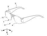
도 1은 본 발명에 따른 디스플레이 장치의 일 실시예이다.
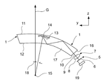
도 2는 이미지-생성 모듈의 대략적인 도시를 포함하는 본 발명에 따른 광학 요소(1)의 부분 확대 단면도이다.
도 3은 광 안내 채널(17) 및 커플링-아웃 섹션(14)의 영역에 있어서 광학 요소(1)의 후면(12)의 대략적인 확대도이다.
도 4는 본 발명에 따른 광학 요소를 생산하기 위한 방법을 설명하는 흐름도이다.
도 5는 본 발명에 따른 광학 요소의 생산을 설명하기 위한 제1 투명 부분 몸체의 확대 단면도이다.
도 6은 적용된 반사 코팅을 가지는 제1 투명 부분 몸체의 단면도이다.
도 7은 적용된 보호 층을 가지는 제1 투명 부분 몸체의 단면도이다.
도 8은 본 발명에 따른 마간된 광학 요소(1)의 대략도이다.
도 9는 보호 층을 적용하는 단계의 변형을 설명하기 위한 제1 투명 부분 몸체의 단면도이다.
도 10은 도 9에 따른 보호 층을 가지는 본 발명에 따른 마감된 광학 요소의 단면도이다.
도 11은 보호 층의 적용을 위한 추가의 실시예를 설명하기 위한 단면도이다.
도 12는 도 11에 따른 보호 층을 가지는 본 발명에 따른 광학 요소의 단면도이다.
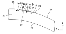
도 13은 본 발명에 따른 광학 요소의 변형의 단면도이다.
Claims (15)
- 미리 결정된 파장 범위에 있어서 투명한 몸체를 포함하는 광학 요소를 생산하기 위한 방법에 있어서, 이때 광학적으로 효과적인 구조가 내재되어 있고, 상기 방법은
a) 미리 결정된 파장 범위에 있어서 투명하고 또한 그 상측에 구조화된 섹션을 포함하는 제1 부분 몸체를 마련하는 단계,
b) 상기 광학적으로 효과적인 구조를 형성하기 위해 상기 미리 결정된 파장 범위에 있어서 광학적으로 효과적인 코팅을 상기 구조화된 섹션에 적용하는 단계, 및
c) 써모플라스틱 물질 및/또는 듀로플라스틱 물질의 캐스팅을 이용해 상기 미리 결정된 파장 범위에 있어서 투명한 커버 층을 상기 제1 부분 몸체의 상기 상측에 적용하는 단계를 포함하는, 방법. - 제 1 항에 있어서, b) 단계 후 c) 단계 전에 듀로플라스틱 물질로 만들어진 보호 층이 캐스팅에 의해 상기 광학적으로 효과적인 코팅에 적용되는, 방법.
- 제 2 항에 있어서, c) 단계에서 상기 커버 층이 상기 보호 층을 포함하는 상기 제1 부분 몸체의 전체 상측 상에 형성되는, 방법.
- 제 1 항 내지 제 3 항 중 어느 한 항에 있어서, 상기 제1 부분 몸체는 제1 폴리머 물질로부터 형성되고 또한 c) 단계에서, 상기 커버 층의 적용을 위해, 제2 폴리머 물질이 상기 제1 부분 몸체의 상기 상측 상에 적용되고 또한 상기 제1 폴리머 물질에 상기 제2 폴리머 물질의 화학적 결합이 초래되는, 방법.
- 제 1 항 내지 제 4 항 중 어느 한 항에 있어서, c) 단계에서, 상기 써모플라스틱 물질이 주입-성형 프로세스(injection-moulding process)를 이용해 적용되는, 방법.
- 제 1 항 내지 제 5 항 중 어느 한 항에 있어서, c) 단계에서, 상기 듀로플라스틱 물질이 RIM 프로세스를 이용해 적용되는, 방법.
- 제 1 항 내지 제 6 항 중 어느 한 항에 있어서, a) 단계에서, 상기 제1 부분 몸체의 준비를 위해, 상기 후자는 RIM 프로세스를 이용해 듀로플라스틱 물질로부터 형성되는, 방법.
- 제 6 항 또는 제 7 항에 있어서, 상기 듀로플라스틱 물질의 적용은 적어도 2 개의 연속된 부분 단계들에서 RIM 프로세스를 이용해 수행되는, 방법.
- 제 1 항 내지 제 8 항 중 어느 한 항에 있어서, 상기 미리 결정된 파장 범위로부터 적어도 소정의 파장에 있어서 그 굴절율들이 0.005보다 더 크지 않은 만큼 다른 이러한 물질들이 제1 및 제2 폴리머 물질로 사용되는, 방법.
- 제 1 항 내지 제 9 항 중 어느 한 항에 있어서, c) 단계에서 상기 커버 층이 형성되어 제1 부분 몸체로부터 멀리 대면하는 상기 커버 층의 경계 표면이 상기 광학 요소의 경계 표면을 형성하는, 방법.
- 제 1 항 내지 제 10 항 중 어느 한 항에 있어서, a) 내지 c) 단계들이 수행되어 상기 광학적으로 효과적인 구조가 상기 투명 몸체 안에 완전히 내재되는, 방법.
- 제 1 항 내지 제 11 항 중 어느 한 항에 있어서, a) 내지 c) 단계들이 수행되어 상기 광학적으로 효과적인 구조가 서로로부터 이격된 반사 표면 조각들을 포함하는, 방법.
- 투명 몸체(20, 28)를 가지는 광학 요소에 있어서, 제1 항 내지 제 12 항 중 한 항의 단계들에 의해 생성되는 광학적으로 효과적인 구조(14)가 내재되어 있는, 광학 요소.
- 제 13 항에 있어서, 이미지를 생성하고 또한 사용자의 머리에 착용될 수 있는 디스플레이 장치(2)를 위한 안경 렌즈로서 형성되고, 또한 전면(11) 및 후면(12),
커플링-인 섹션(16) 및 상기 커플링-인 섹션(16)으로부터 이격되어 있는 커플링-아웃 섹션(14) 및
상기 생성된 이미지의 화소들의 광 번들들(9)을 안내하기에 적절한 광 안내 채널(17)을 포함하고, 상기 광 번들들(9)은 상기 광학 요소(1)에서 상기 커플링-아웃 섹션(14)으로, 상기 광학 요소(1)의 상기 커플링-인 섹션(16)을 거쳐 상기 광학 요소(1)로 커플링되고, 이로써 이들은 상기 광학 요소(1)로부터 커플링 아웃되고, 상기 커플링-아웃 섹션(14)은 상기 광학적으로 효과적인 구조를 포함하고, 이것은 상기 커플링-아웃으로 상기 광 번들들(9)의 굴절을 초래하는, 광학 요소. - 사용자의 머리에 착용될 수 있는 홀더(3),
이미지를 생성하는, 상기 홀더(3)에 고정되는 이미지-생성 모듈(5), 및
제 14 항에 따른 광학 요소(1)를 포함하고, 상기 홀더(3)가 상기 사용자의 머리에 착용된 때, 상기 사용자가 이를 가상 이미지로서 인식할 수 있도록 상기 생성된 이미지를 이미징하는, 상기 홀더(3)에 고정되는 이미징 광학 시스템을 가지는 디스플레이 장치.
Applications Claiming Priority (3)
| Application Number | Priority Date | Filing Date | Title |
|---|---|---|---|
| DE102014113966.6 | 2014-09-26 | ||
| DE102014113966.6A DE102014113966A1 (de) | 2014-09-26 | 2014-09-26 | Verfahren zum Herstellen eines Optikelementes |
| PCT/EP2015/071590 WO2016046125A2 (de) | 2014-09-26 | 2015-09-21 | Verfahren zum herstellen eines optikelementes |
Publications (2)
| Publication Number | Publication Date |
|---|---|
| KR20170063577A true KR20170063577A (ko) | 2017-06-08 |
| KR102492422B1 KR102492422B1 (ko) | 2023-01-26 |
Family
ID=54260726
Family Applications (1)
| Application Number | Title | Priority Date | Filing Date |
|---|---|---|---|
| KR1020177007209A Active KR102492422B1 (ko) | 2014-09-26 | 2015-09-21 | 광학 요소를 생산하기 위한 방법 |
Country Status (7)
| Country | Link |
|---|---|
| US (1) | US10558045B2 (ko) |
| EP (1) | EP3198312A2 (ko) |
| JP (1) | JP6943763B2 (ko) |
| KR (1) | KR102492422B1 (ko) |
| CN (2) | CN115657179A (ko) |
| DE (1) | DE102014113966A1 (ko) |
| WO (1) | WO2016046125A2 (ko) |
Cited By (1)
| Publication number | Priority date | Publication date | Assignee | Title |
|---|---|---|---|---|
| KR20220002006A (ko) * | 2020-06-30 | 2022-01-06 | 엘지디스플레이 주식회사 | 전계발광표시패널을 포함하는 착용형 표시장치 |
Families Citing this family (6)
| Publication number | Priority date | Publication date | Assignee | Title |
|---|---|---|---|---|
| DE102015102032A1 (de) | 2015-02-12 | 2016-08-18 | Carl Zeiss Jena Gmbh | Optisches Element |
| CN107272319A (zh) * | 2016-04-07 | 2017-10-20 | 中强光电股份有限公司 | 投影装置以及影像投影方法 |
| DE102018002384C5 (de) | 2018-03-22 | 2022-03-10 | Shape Engineering GmbH | Verfahren zur Herstellung eines Brillenglases |
| KR102375853B1 (ko) * | 2019-04-25 | 2022-03-17 | 주식회사 엘지화학 | 회절 도광판 및 회절 도광판의 제조 방법 |
| WO2021029693A1 (ko) * | 2019-08-14 | 2021-02-18 | 주식회사 엘지화학 | 회절 도광판 및 회절 도광판의 제조 방법 |
| CN115552300A (zh) | 2020-05-14 | 2022-12-30 | 奇跃公司 | 用于将折射光学器件与衍射目镜波导显示器集成的方法和系统 |
Citations (6)
| Publication number | Priority date | Publication date | Assignee | Title |
|---|---|---|---|---|
| US20100011637A1 (en) * | 2008-07-15 | 2010-01-21 | Yudong Zhang | Displaying device and method thereof |
| JP2012068441A (ja) * | 2010-09-24 | 2012-04-05 | Seiko Epson Corp | 導光板の製造方法 |
| JP2012198264A (ja) * | 2011-03-18 | 2012-10-18 | Seiko Epson Corp | 導光板の製造方法及び導光板並びに導光板を備える虚像表示装置 |
| JP2013073070A (ja) * | 2011-09-28 | 2013-04-22 | Toshiba Corp | 表示装置 |
| WO2014020073A1 (de) * | 2012-08-02 | 2014-02-06 | Carl Zeiss Ag | Anzeigevorrichtung |
| US20140043850A1 (en) * | 2012-08-13 | 2014-02-13 | 3M Innovative Properties Company | Lighting devices with patterned printing of diffractive extraction features |
Family Cites Families (17)
| Publication number | Priority date | Publication date | Assignee | Title |
|---|---|---|---|---|
| EP0045305A4 (en) | 1979-10-22 | 1983-10-06 | Singer Co | SEGMENTED DISC CONSTRUCTION. |
| CA2120877A1 (en) * | 1993-04-28 | 1994-10-29 | Jesse D. Wolfe | Durable first and second surface mirrors |
| US6231183B1 (en) | 1999-07-06 | 2001-05-15 | Stephen M. Dillon | Optical lens structure and method of fabrication thereof |
| EP1849033B1 (en) | 2005-02-10 | 2019-06-19 | Lumus Ltd | Substrate-guided optical device utilizing thin transparent layer |
| US20060192306A1 (en) | 2005-02-25 | 2006-08-31 | The Microoptical Corporation | Manufacturing methods for embedded optical system |
| CN1834701A (zh) * | 2005-03-16 | 2006-09-20 | 亚洲光学股份有限公司 | 反射镜及其制造方法 |
| FR2886574B1 (fr) | 2005-06-06 | 2009-07-10 | Essilor Int | Moule et procede de moulage, notamment par moulage par injection reactive, en particulier d'un element optique en materiau polymere |
| US8077392B2 (en) * | 2006-06-13 | 2011-12-13 | Panasonic Corporation | Composite optical element |
| KR20120123741A (ko) * | 2010-01-13 | 2012-11-09 | 쓰리엠 이노베이티브 프로퍼티즈 컴파니 | 미세 구조화 저 굴절률 나노공극형 층을 갖는 광학 필름 및 이의 제조 방법 |
| US8810913B2 (en) | 2010-01-25 | 2014-08-19 | Bae Systems Plc | Projection display |
| EP2352042B1 (en) * | 2010-01-29 | 2017-05-17 | Dexerials Corporation | Optical element and method for manufacturing the same |
| JP2012021936A (ja) * | 2010-07-16 | 2012-02-02 | Toshiba Corp | 光導波路型センサチップおよび光導波路型センサ |
| US9223137B2 (en) | 2010-10-08 | 2015-12-29 | Seiko Epson Corporation | Virtual image display apparatus |
| JP5703876B2 (ja) * | 2011-03-18 | 2015-04-22 | セイコーエプソン株式会社 | 導光板及びこれを備える虚像表示装置並びに導光板の製造方法 |
| IN2014CN02023A (ko) | 2011-08-19 | 2015-05-29 | Visual Physics Llc | |
| US9242418B2 (en) | 2011-11-16 | 2016-01-26 | Essilor International | Ophthalmic lens containing a fresnel surface and method for manufacturing same |
| US8665178B1 (en) * | 2012-03-01 | 2014-03-04 | Google, Inc. | Partially-reflective waveguide stack and heads-up display using same |
-
2014
- 2014-09-26 DE DE102014113966.6A patent/DE102014113966A1/de active Pending
-
2015
- 2015-09-21 KR KR1020177007209A patent/KR102492422B1/ko active Active
- 2015-09-21 CN CN202211178391.7A patent/CN115657179A/zh active Pending
- 2015-09-21 CN CN201580051164.XA patent/CN107003446A/zh active Pending
- 2015-09-21 JP JP2017516145A patent/JP6943763B2/ja active Active
- 2015-09-21 US US15/514,514 patent/US10558045B2/en active Active
- 2015-09-21 WO PCT/EP2015/071590 patent/WO2016046125A2/de not_active Ceased
- 2015-09-21 EP EP15775647.9A patent/EP3198312A2/de active Pending
Patent Citations (6)
| Publication number | Priority date | Publication date | Assignee | Title |
|---|---|---|---|---|
| US20100011637A1 (en) * | 2008-07-15 | 2010-01-21 | Yudong Zhang | Displaying device and method thereof |
| JP2012068441A (ja) * | 2010-09-24 | 2012-04-05 | Seiko Epson Corp | 導光板の製造方法 |
| JP2012198264A (ja) * | 2011-03-18 | 2012-10-18 | Seiko Epson Corp | 導光板の製造方法及び導光板並びに導光板を備える虚像表示装置 |
| JP2013073070A (ja) * | 2011-09-28 | 2013-04-22 | Toshiba Corp | 表示装置 |
| WO2014020073A1 (de) * | 2012-08-02 | 2014-02-06 | Carl Zeiss Ag | Anzeigevorrichtung |
| US20140043850A1 (en) * | 2012-08-13 | 2014-02-13 | 3M Innovative Properties Company | Lighting devices with patterned printing of diffractive extraction features |
Cited By (1)
| Publication number | Priority date | Publication date | Assignee | Title |
|---|---|---|---|---|
| KR20220002006A (ko) * | 2020-06-30 | 2022-01-06 | 엘지디스플레이 주식회사 | 전계발광표시패널을 포함하는 착용형 표시장치 |
Also Published As
| Publication number | Publication date |
|---|---|
| EP3198312A2 (de) | 2017-08-02 |
| CN115657179A (zh) | 2023-01-31 |
| WO2016046125A3 (de) | 2016-07-07 |
| JP6943763B2 (ja) | 2021-10-06 |
| CN107003446A (zh) | 2017-08-01 |
| KR102492422B1 (ko) | 2023-01-26 |
| WO2016046125A2 (de) | 2016-03-31 |
| DE102014113966A1 (de) | 2016-03-31 |
| US10558045B2 (en) | 2020-02-11 |
| US20170227775A1 (en) | 2017-08-10 |
| JP2017530406A (ja) | 2017-10-12 |
Similar Documents
| Publication | Publication Date | Title |
|---|---|---|
| US10754157B2 (en) | Optical element | |
| KR102492422B1 (ko) | 광학 요소를 생산하기 위한 방법 | |
| CN112888973B (zh) | 包含光学元件的改进的光学制品及其制造方法 | |
| US10274749B2 (en) | Producing microstructured spectacle lenses by means of transfer layer | |
| JP6207622B2 (ja) | アイウエア用偏光レンズの製造方法 | |
| JP7749294B2 (ja) | 屈折光学系と回折接眼レンズ導波管ディスプレイの統合のための方法およびシステム | |
| JP2019512717A (ja) | 光学的撮像素子用の眼鏡レンズ、および拡張現実眼鏡 | |
| US20150277144A1 (en) | Production of opththalmic lenses with protected microstructures | |
| KR20190060866A (ko) | 안경 렌즈 및 그 생산 방법 | |
| CN115509030A (zh) | 高折射率偏振眼镜镜片 | |
| KR102587000B1 (ko) | 광학적 요소 | |
| JP2025536588A (ja) | 光学歪みを低減するための偏光pvaウェハ |
Legal Events
| Date | Code | Title | Description |
|---|---|---|---|
| PA0105 | International application |
Patent event date: 20170315 Patent event code: PA01051R01D Comment text: International Patent Application |
|
| PG1501 | Laying open of application | ||
| PA0201 | Request for examination |
Patent event code: PA02012R01D Patent event date: 20200410 Comment text: Request for Examination of Application |
|
| E902 | Notification of reason for refusal | ||
| PE0902 | Notice of grounds for rejection |
Comment text: Notification of reason for refusal Patent event date: 20210708 Patent event code: PE09021S01D |
|
| E902 | Notification of reason for refusal | ||
| PE0902 | Notice of grounds for rejection |
Comment text: Notification of reason for refusal Patent event date: 20220125 Patent event code: PE09021S01D |
|
| E902 | Notification of reason for refusal | ||
| PE0902 | Notice of grounds for rejection |
Comment text: Notification of reason for refusal Patent event date: 20220817 Patent event code: PE09021S01D |
|
| E701 | Decision to grant or registration of patent right | ||
| PE0701 | Decision of registration |
Patent event code: PE07011S01D Comment text: Decision to Grant Registration Patent event date: 20221021 |
|
| GRNT | Written decision to grant | ||
| PR0701 | Registration of establishment |
Comment text: Registration of Establishment Patent event date: 20230120 Patent event code: PR07011E01D |
|
| PR1002 | Payment of registration fee |
Payment date: 20230120 End annual number: 3 Start annual number: 1 |
|
| PG1601 | Publication of registration |