KR20170064532A - 고속 통신 잭 - Google Patents
고속 통신 잭 Download PDFInfo
- Publication number
- KR20170064532A KR20170064532A KR1020177006027A KR20177006027A KR20170064532A KR 20170064532 A KR20170064532 A KR 20170064532A KR 1020177006027 A KR1020177006027 A KR 1020177006027A KR 20177006027 A KR20177006027 A KR 20177006027A KR 20170064532 A KR20170064532 A KR 20170064532A
- Authority
- KR
- South Korea
- Prior art keywords
- layer
- trace
- jack
- housing
- circuit board
- Prior art date
- Legal status (The legal status is an assumption and is not a legal conclusion. Google has not performed a legal analysis and makes no representation as to the accuracy of the status listed.)
- Ceased
Links
Images








Classifications
-
- H—ELECTRICITY
- H01—ELECTRIC ELEMENTS
- H01R—ELECTRICALLY-CONDUCTIVE CONNECTIONS; STRUCTURAL ASSOCIATIONS OF A PLURALITY OF MUTUALLY-INSULATED ELECTRICAL CONNECTING ELEMENTS; COUPLING DEVICES; CURRENT COLLECTORS
- H01R24/00—Two-part coupling devices, or either of their cooperating parts, characterised by their overall structure
- H01R24/60—Contacts spaced along planar side wall transverse to longitudinal axis of engagement
- H01R24/62—Sliding engagements with one side only, e.g. modular jack coupling devices
- H01R24/64—Sliding engagements with one side only, e.g. modular jack coupling devices for high frequency, e.g. RJ 45
-
- H—ELECTRICITY
- H01—ELECTRIC ELEMENTS
- H01R—ELECTRICALLY-CONDUCTIVE CONNECTIONS; STRUCTURAL ASSOCIATIONS OF A PLURALITY OF MUTUALLY-INSULATED ELECTRICAL CONNECTING ELEMENTS; COUPLING DEVICES; CURRENT COLLECTORS
- H01R13/00—Details of coupling devices of the kinds covered by groups H01R12/70 or H01R24/00 - H01R33/00
- H01R13/646—Details of coupling devices of the kinds covered by groups H01R12/70 or H01R24/00 - H01R33/00 specially adapted for high-frequency, e.g. structures providing an impedance match or phase match
- H01R13/6461—Means for preventing cross-talk
- H01R13/6464—Means for preventing cross-talk by adding capacitive elements
- H01R13/6466—Means for preventing cross-talk by adding capacitive elements on substrates, e.g. printed circuit boards [PCB]
-
- H—ELECTRICITY
- H01—ELECTRIC ELEMENTS
- H01R—ELECTRICALLY-CONDUCTIVE CONNECTIONS; STRUCTURAL ASSOCIATIONS OF A PLURALITY OF MUTUALLY-INSULATED ELECTRICAL CONNECTING ELEMENTS; COUPLING DEVICES; CURRENT COLLECTORS
- H01R13/00—Details of coupling devices of the kinds covered by groups H01R12/70 or H01R24/00 - H01R33/00
- H01R13/648—Protective earth or shield arrangements on coupling devices, e.g. anti-static shielding
- H01R13/658—High frequency shielding arrangements, e.g. against EMI [Electro-Magnetic Interference] or EMP [Electro-Magnetic Pulse]
- H01R13/6581—Shield structure
- H01R13/6585—Shielding material individually surrounding or interposed between mutually spaced contacts
-
- H—ELECTRICITY
- H01—ELECTRIC ELEMENTS
- H01R—ELECTRICALLY-CONDUCTIVE CONNECTIONS; STRUCTURAL ASSOCIATIONS OF A PLURALITY OF MUTUALLY-INSULATED ELECTRICAL CONNECTING ELEMENTS; COUPLING DEVICES; CURRENT COLLECTORS
- H01R13/00—Details of coupling devices of the kinds covered by groups H01R12/70 or H01R24/00 - H01R33/00
- H01R13/648—Protective earth or shield arrangements on coupling devices, e.g. anti-static shielding
- H01R13/658—High frequency shielding arrangements, e.g. against EMI [Electro-Magnetic Interference] or EMP [Electro-Magnetic Pulse]
- H01R13/6598—Shield material
- H01R13/6599—Dielectric material made conductive, e.g. plastic material coated with metal
-
- H—ELECTRICITY
- H01—ELECTRIC ELEMENTS
- H01R—ELECTRICALLY-CONDUCTIVE CONNECTIONS; STRUCTURAL ASSOCIATIONS OF A PLURALITY OF MUTUALLY-INSULATED ELECTRICAL CONNECTING ELEMENTS; COUPLING DEVICES; CURRENT COLLECTORS
- H01R43/00—Apparatus or processes specially adapted for manufacturing, assembling, maintaining, or repairing of line connectors or current collectors or for joining electric conductors
- H01R43/16—Apparatus or processes specially adapted for manufacturing, assembling, maintaining, or repairing of line connectors or current collectors or for joining electric conductors for manufacturing contact members, e.g. by punching and by bending
-
- H—ELECTRICITY
- H05—ELECTRIC TECHNIQUES NOT OTHERWISE PROVIDED FOR
- H05K—PRINTED CIRCUITS; CASINGS OR CONSTRUCTIONAL DETAILS OF ELECTRIC APPARATUS; MANUFACTURE OF ASSEMBLAGES OF ELECTRICAL COMPONENTS
- H05K1/00—Printed circuits
- H05K1/02—Details
- H05K1/0213—Electrical arrangements not otherwise provided for
- H05K1/0216—Reduction of cross-talk, noise or electromagnetic interference
- H05K1/0218—Reduction of cross-talk, noise or electromagnetic interference by printed shielding conductors, ground planes or power plane
-
- H—ELECTRICITY
- H05—ELECTRIC TECHNIQUES NOT OTHERWISE PROVIDED FOR
- H05K—PRINTED CIRCUITS; CASINGS OR CONSTRUCTIONAL DETAILS OF ELECTRIC APPARATUS; MANUFACTURE OF ASSEMBLAGES OF ELECTRICAL COMPONENTS
- H05K1/00—Printed circuits
- H05K1/02—Details
- H05K1/0213—Electrical arrangements not otherwise provided for
- H05K1/0216—Reduction of cross-talk, noise or electromagnetic interference
- H05K1/0228—Compensation of cross-talk by a mutually correlated lay-out of printed circuit traces, e.g. for compensation of cross-talk in mounted connectors
-
- H—ELECTRICITY
- H05—ELECTRIC TECHNIQUES NOT OTHERWISE PROVIDED FOR
- H05K—PRINTED CIRCUITS; CASINGS OR CONSTRUCTIONAL DETAILS OF ELECTRIC APPARATUS; MANUFACTURE OF ASSEMBLAGES OF ELECTRICAL COMPONENTS
- H05K1/00—Printed circuits
- H05K1/02—Details
- H05K1/0213—Electrical arrangements not otherwise provided for
- H05K1/0237—High frequency adaptations
- H05K1/0245—Lay-out of balanced signal pairs, e.g. differential lines or twisted lines
-
- H—ELECTRICITY
- H05—ELECTRIC TECHNIQUES NOT OTHERWISE PROVIDED FOR
- H05K—PRINTED CIRCUITS; CASINGS OR CONSTRUCTIONAL DETAILS OF ELECTRIC APPARATUS; MANUFACTURE OF ASSEMBLAGES OF ELECTRICAL COMPONENTS
- H05K1/00—Printed circuits
- H05K1/02—Details
- H05K1/0213—Electrical arrangements not otherwise provided for
- H05K1/0237—High frequency adaptations
- H05K1/025—Impedance arrangements, e.g. impedance matching, reduction of parasitic impedance
-
- H—ELECTRICITY
- H05—ELECTRIC TECHNIQUES NOT OTHERWISE PROVIDED FOR
- H05K—PRINTED CIRCUITS; CASINGS OR CONSTRUCTIONAL DETAILS OF ELECTRIC APPARATUS; MANUFACTURE OF ASSEMBLAGES OF ELECTRICAL COMPONENTS
- H05K1/00—Printed circuits
- H05K1/02—Details
- H05K1/0277—Bendability or stretchability details
- H05K1/028—Bending or folding regions of flexible printed circuits
-
- H—ELECTRICITY
- H05—ELECTRIC TECHNIQUES NOT OTHERWISE PROVIDED FOR
- H05K—PRINTED CIRCUITS; CASINGS OR CONSTRUCTIONAL DETAILS OF ELECTRIC APPARATUS; MANUFACTURE OF ASSEMBLAGES OF ELECTRICAL COMPONENTS
- H05K1/00—Printed circuits
- H05K1/02—Details
- H05K1/14—Structural association of two or more printed circuits
- H05K1/147—Structural association of two or more printed circuits at least one of the printed circuits being bent or folded, e.g. by using a flexible printed circuit
-
- H—ELECTRICITY
- H01—ELECTRIC ELEMENTS
- H01R—ELECTRICALLY-CONDUCTIVE CONNECTIONS; STRUCTURAL ASSOCIATIONS OF A PLURALITY OF MUTUALLY-INSULATED ELECTRICAL CONNECTING ELEMENTS; COUPLING DEVICES; CURRENT COLLECTORS
- H01R2107/00—Four or more poles
Landscapes
- Engineering & Computer Science (AREA)
- Microelectronics & Electronic Packaging (AREA)
- Physics & Mathematics (AREA)
- Electromagnetism (AREA)
- Manufacturing & Machinery (AREA)
- Details Of Connecting Devices For Male And Female Coupling (AREA)
- Coupling Device And Connection With Printed Circuit (AREA)
- Connector Housings Or Holding Contact Members (AREA)
- Manufacturing Of Electrical Connectors (AREA)
Abstract
Description
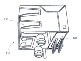
도 2는 도 1의 RJ45 잭의 좌측부분의 저면 사시도이다.
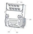
도 3은 도 1의 RJ45 잭 및 연성 프린트 회로 기판에 대한 차폐를 제공하기 위한 잭 쉴드의 우측 저면도이다.
도 4A는 도 1의 프린트 회로 기판의 앞면의 평면도이다.
도 4B는 또 다른 실시예의 프린트 회로 기판의 앞면의 평면도이다.
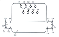
도 5A는 도 4의 프린트 회로기판의 뒷면의 평면도이다.
도 5B는 또 다른 실시예의 프린트 회로기판의 뒷면의 평면도이다.
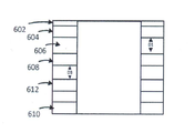
도 6A는 도 4의 프린트 회로기판의 선 BB를 따른 단면도이다.
도 6B는 도 4의 프린트 회로기판의 바이어의 단면도이다.
도 6C는 도 4의 프린트 회로기판의 또 다른 실시예에 따른 바이어의 단면도이다.
도 7은 서로 매칭되며 평형된 전송 및 수신 케이블 쌍을 갖는 RJ45 잭의 개략도이다.
도 8은 차동적으로 평형된 신호선 쌍의 개략도이다,
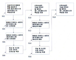
도 9는 제1 신호와 제2 신호에 기초하여 도 4의 두 트레이스를 차동적으로 평형시키기 위해 사용된 프로세스의 개략도이다.
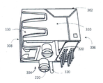
도 10A는 쉴드가 제거된, 도 1의 RJ45 잭의 후방 사시도이다.
도 10B는 쉴드가 제거된, 또 다른 실시예의 도 1의 RJ45 잭의 후방 사시도이다.
Claims (20)
- 플러그를 수용하는 포트를 포함하되 이 포트는 플러그의 해당 신호 선에 각각 연결되는 복수의 핀을 포함하는 하우징;
하우징을 둘러싸는 차폐함;
하우징과 차폐함 사이의 연성 회로 보드;를 포함하며, 이 회로보드는
기판,
각 바이어가 하우징의 핀을 수용하도록 기판을 통하여 연장되는 복수의 바이어,
기판의 제1측 상에 위치하며 복수의 바이어의 각 바이어로부터 연장되는 복수의 트레이스, 및
기판의 제1 측에 대향하는 기판의 제2 측 상의 차폐면을 갖는 고속 통신 잭. - 제 1항에 있어서, 활성화되었을 때 각 트레이스가 제2의 인접하는 트레이스와 차동적으로 매칭되는 잭.
- 제 2항에 있어서, 매칭된 트레이스 쌍의 제1 트레이스의 임피던스가 매칭된 트레이스 쌍의 제2 트레이스의 임피던스 값과 실질적으로 동일하도록 조절되는 잭.
- 제 1항에 있어서, 커패시터가 트레이스 층과 유전체 층에 매입된 복귀신호 층에 의해 각 바이어에 형성되는 잭.
- 제 4항에 있어서, 커패시터가 약 0.1pf와 약 0.5pf 사이의 값을 갖도록 복귀신호 층과 트레이스 층 사이의 거리가 조절되는 잭.
- 제 3항에 있어서, 매칭된 트레이스 쌍의 각 트레이스의 폭, 높이, 또느 길이가 제1 트레이스의 임피던스가 제2 트레이스의 임피던스와 매칭하도록 조절되는 잭.
- 제 4항에 있어서, 제2 복귀신호 층이 제1 복귀신호 층 아래의 유전체 층에 형성되어서 제2 커패시터를 형성하는 잭.
- 제 7항에 있어서, 제1 신호 층과 제2 신호 층 사이의 거리가 0.1pf와 0.5pf 사이의 제2 커패시터 값을 갖도록 조절되는 잭.
- 제 3항에 있어서, 제1 트레이스와 제2 트레이스의 임피던스가, 제1 신호가 제1 트레이스에 전송되고 제2 신호가 제2 트레이스에 전송될 때, 트레이스들이 매칭되도록 조절되는 잭.
- 제 4항에 있어서, 커패시터, 트레이스, 및 복귀신호 층이 매칭된 트레이스 세트에 의해 공통모드 필터를 형성하는 잭.
- 제 10항에 있어서, 커패시터의 값이, 공통모드 필터가 매칭된 트레이스로부터의 신호 반사를 방지하도록 조절되는 잭.
- 제 11항에 있어서, 제1 차폐 탭에 대향하는 기판 측에 제2 차폐 탭을 포함하는 잭.
- 제 1항에 있어서, 트레이스가 금으로 도금되는 잭.
- 제 1항에 있어서, 기판이 3.0 보다 큰 유전상수를 갖는 유전체 재료를 포함하는 잭.
- 플러그를 수용하는 포트를 포함하되, 이 포트는 플러그의 해당 신호 선에 각각 연결되는 복수의 핀을 갖는 표준 RJ45 하우징을 포함하는 고속통신 잭으로서,
하우징을 둘러싸는 차폐함,
하우징과 차폐함 사이의 연성 회로 보드를 포함하되, 이 회로보드는
기판,
각 바이어가 하우징의 핀을 수용하도록 기판을 통하여 연장되는 복수의 바이어,
기판의 제1측 상에 위치하며 복수의 바이어의 각 바이어로부터 연장되는 복수의 트레이스, 및
기판의 제1 측에 대향하는 기판의 제2 측상의 차폐면을 갖는 고속 통신 잭. - 앞면, 뒷면, 윗면, 밑면, 우측면, 및 좌측면을 갖는 표준 RJ45 하우징을 사용하되, 이 하우징은 플러그의 해당 신호 선에 각각 연결되는 복수의 핀을 갖는 고속통신 잭의 제조방법에 있어서,
기판, 각 바이어가 하우징의 핀을 수용하도록 기판을 통하여 연장되는 복수의 바이어, 각 트레이스가 복수의 바이어의 각 바이어로부터 연장되며 기판의 제1측 상에 위치하는 복수의 트레이스, 기판의 제1 측에 대향하는 기판의 제2 측상의 차폐면, 및 연성 회로보드의 대향하는 단부들 상에 위치하며 차폐 트레이스에 의해 전기회로 보드에 연결되는 적어도 2개의 차폐 탭을 갖는 연성 회로보드를 형성하는 단계,
하우징의 해당 핀으로 연성 회로보드의 각 바이어를 삽입하는 단계,
바이어를 갖는 연성 회로 보드의 일 부분이 하우징의 뒷 부분에 위치한 차폐면을 갖는 연성 회로 보드의 부분에 수직하도록 연성 회로 보드를 만곡시키는 단계,
하나는 하우징의 우측면과 접하고 하나는 좌측면과 접하도록 각 차폐 탭을 만곡시키는 단계, 및
차폐함이 차폐 탭의 각각과 접하도록 차폐함을 연성 회로 보드와 하우징 위에 형성시키는 단계로 구성되는 고속통신 잭의 제조방법. - 플러그를 수용하는 포트를 포함하되 이 포트는 플러그의 해당 신호 선에 각각 연결되는 복수의 핀을 포함하는 하우징,
하우징을 둘러싸는 차폐함,
차폐함과 하우징 사이의 다층 연성 회로 보드, 이 다층 회로 보드는 복수의 트레이스를 갖는 제1 층, 제1 층의 일측에 위치되되 트레이스에 대향하도록 위치되는 유전체 재료의 제2층, 제2 층의 일측에 위치되되 제1 층에 대향하도록 위치되며 전도체 재료로 만들어지는 복귀면을 갖는 제3 층, 제3 층의 일측에 위치되되 제2 층에 대향하도록 위치되며 유전체 재료로 만들어지는 제4층, 및 제4 층의 일측에 위치되되 제3 층에 대향하도록 위치되며 전도체 재료로 만들어지는 제5층을 가지며,
각 바이어가 하우징의 핀을 수용하도록 제1, 제2, 제3, 제4, 및 제5 기판을 통하여 연장되는 복수의 바이어를 포함하는 고속 통신 잭. - 제 17항에 있어서, 커패시터가 제1, 제2, 및 제 3층의 복수의 트레이스 중 하나와의 조합에 의해 각 바이어에 형성되는 잭.
- 제 18항에 있어서, 각 바이어의 커패시터가 약 0.1pf와 약 0.5pf 사이의 값을 갖도록 제2 층의 깊이가 조절되는 잭.
- 제 17항에 있어서, 제4 층과 제5 층 사이에 형성되되 전도체 재료로 만들어지는 제 6층, 및 제 6층과 제5 층 사이에 형성되되 유전체 재료로 만들어지는 제7층을 더욱 포함하는 잭.
Applications Claiming Priority (3)
| Application Number | Priority Date | Filing Date | Title |
|---|---|---|---|
| US14/504,088 US9337592B2 (en) | 2012-02-13 | 2014-10-01 | High speed communication jack |
| US14/504,088 | 2014-10-01 | ||
| PCT/US2015/050599 WO2016053632A1 (en) | 2014-10-01 | 2015-09-17 | High speed communication jack |
Publications (1)
| Publication Number | Publication Date |
|---|---|
| KR20170064532A true KR20170064532A (ko) | 2017-06-09 |
Family
ID=55631255
Family Applications (1)
| Application Number | Title | Priority Date | Filing Date |
|---|---|---|---|
| KR1020177006027A Ceased KR20170064532A (ko) | 2014-10-01 | 2015-09-17 | 고속 통신 잭 |
Country Status (13)
| Country | Link |
|---|---|
| US (2) | US9899776B2 (ko) |
| EP (1) | EP3201995A4 (ko) |
| JP (1) | JP2017534141A (ko) |
| KR (1) | KR20170064532A (ko) |
| CN (1) | CN107078440A (ko) |
| AU (1) | AU2015324371B2 (ko) |
| BR (1) | BR112017006086A2 (ko) |
| CA (1) | CA2960385C (ko) |
| IL (1) | IL250842B (ko) |
| MX (1) | MX2017002959A (ko) |
| PH (1) | PH12017500504A1 (ko) |
| RU (1) | RU2017114931A (ko) |
| WO (1) | WO2016053632A1 (ko) |
Families Citing this family (1)
| Publication number | Priority date | Publication date | Assignee | Title |
|---|---|---|---|---|
| US10050383B2 (en) * | 2015-05-19 | 2018-08-14 | Panduit Corp. | Communication connectors |
Family Cites Families (42)
| Publication number | Priority date | Publication date | Assignee | Title |
|---|---|---|---|---|
| US5269705A (en) * | 1992-11-03 | 1993-12-14 | The Whitaker Corporation | Tape filter and method of applying same to an electrical connector |
| JPH08339873A (ja) * | 1995-06-09 | 1996-12-24 | Nippon Carbide Ind Co Inc | フィルタ付きモジュラーコネクタ |
| US6250968B1 (en) * | 1999-07-14 | 2001-06-26 | Berg Technology, Inc. | Electrical connector system with cross-talk compensation |
| US6350152B1 (en) * | 2000-08-23 | 2002-02-26 | Berg Technology Inc. | Stacked electrical connector for use with a filter insert |
| JP3901004B2 (ja) | 2001-06-13 | 2007-04-04 | セイコーエプソン株式会社 | 電気光学装置及びその製造方法、並びに電子機器 |
| JP2003015902A (ja) | 2001-07-03 | 2003-01-17 | Sony Corp | 試験装置 |
| US6881096B2 (en) * | 2002-04-15 | 2005-04-19 | Lantronix, Inc. | Compact serial-to-ethernet conversion port |
| US7474737B2 (en) | 2002-10-10 | 2009-01-06 | The Siemon Company | Telecommunications test plugs having tuned near end crosstalk |
| US6769937B1 (en) | 2003-05-13 | 2004-08-03 | Molex Incorporated | Modular jack assembly for jack plugs with varying numbers of wires |
| US7182649B2 (en) | 2003-12-22 | 2007-02-27 | Panduit Corp. | Inductive and capacitive coupling balancing electrical connector |
| US7179131B2 (en) | 2004-02-12 | 2007-02-20 | Panduit Corp. | Methods and apparatus for reducing crosstalk in electrical connectors |
| CN102082367B (zh) | 2004-03-12 | 2013-11-20 | 泛达公司 | 减小电连接器中串扰的方法及装置 |
| CA2464834A1 (en) | 2004-04-19 | 2005-10-19 | Nordx/Cdt Inc. | Connector |
| JP4777984B2 (ja) * | 2004-07-13 | 2011-09-21 | パンドウィット・コーポレーション | フレキシブルプリント回路板を備えた通信コネクタ |
| US7264516B2 (en) | 2004-12-06 | 2007-09-04 | Commscope, Inc. | Communications jack with printed wiring board having paired coupling conductors |
| US7204722B2 (en) | 2004-12-07 | 2007-04-17 | Commscope Solutions Properties, Llc | Communications jack with compensation for differential to differential and differential to common mode crosstalk |
| US7320624B2 (en) | 2004-12-16 | 2008-01-22 | Commscope, Inc. Of North Carolina | Communications jacks with compensation for differential to differential and differential to common mode crosstalk |
| ATE537586T1 (de) | 2005-07-15 | 2011-12-15 | Panduit Corp | Kommunikationsverbinder mit einer vorrichtung zur kompensation von uebersprechen |
| JP2009527079A (ja) | 2006-02-13 | 2009-07-23 | パンデュイット・コーポレーション | 漏話補償機能付きコネクタ |
| US7402085B2 (en) * | 2006-04-11 | 2008-07-22 | Adc Gmbh | Telecommunications jack with crosstalk compensation provided on a multi-layer circuit board |
| US7364470B2 (en) * | 2006-07-05 | 2008-04-29 | Commscope, Inc. Of North Carolina | Communications connectors with signal current splitting |
| FR2906939B1 (fr) | 2006-10-09 | 2009-01-23 | Legrand France | Dispositif de raccordement pour reseau local |
| WO2008076813A2 (en) | 2006-12-13 | 2008-06-26 | Panduit Corp. | Communication jack having layered plug interface contacts |
| DE102007005959A1 (de) | 2007-02-06 | 2008-08-14 | Adc Gmbh | Steckverbinder |
| MX2010001211A (es) | 2007-08-01 | 2010-03-11 | Belden Cdt Canada Inc | Conector con contacto penetrante aislante. |
| US7967645B2 (en) | 2007-09-19 | 2011-06-28 | Leviton Manufacturing Co., Inc. | High speed data communications connector circuits, systems, and methods for reducing crosstalk in communications systems |
| KR20100074141A (ko) | 2007-09-19 | 2010-07-01 | 레비톤 메뉴팩튜어링 캄파니 인코포레이티드 | 통신 콘센트 내에 위치된 플렉서블 인쇄회로보드 상에 형성되는 내부 누화 보상 회로와 이에 관련된 방법 및 시스템 |
| US7736195B1 (en) | 2009-03-10 | 2010-06-15 | Leviton Manufacturing Co., Inc. | Circuits, systems and methods for implementing high speed data communications connectors that provide for reduced modal alien crosstalk in communications systems |
| CN102007651B (zh) * | 2007-12-19 | 2013-06-26 | 泛达公司 | 用于减少插头/插孔连接内产生共模信号的方法和系统 |
| WO2009118935A1 (ja) | 2008-03-26 | 2009-10-01 | イビデン株式会社 | フレックスリジッド配線板及びその製造方法 |
| US7601034B1 (en) | 2008-05-07 | 2009-10-13 | Ortronics, Inc. | Modular insert and jack including moveable reactance section |
| US7914345B2 (en) | 2008-08-13 | 2011-03-29 | Tyco Electronics Corporation | Electrical connector with improved compensation |
| CN102124609B (zh) * | 2008-08-20 | 2013-09-11 | 泛达公司 | 具有多级补偿的高速连接器 |
| US8167661B2 (en) | 2008-12-02 | 2012-05-01 | Panduit Corp. | Method and system for improving crosstalk attenuation within a plug/jack connection and between nearby plug/jack combinations |
| CA2647704A1 (en) | 2008-12-22 | 2010-06-22 | Belden Cdt (Canada) Inc. | Coupler connector |
| US8047879B2 (en) * | 2009-01-26 | 2011-11-01 | Commscope, Inc. Of North Carolina | Printed wiring boards and communication connectors having series inductor-capacitor crosstalk compensation circuits that share a common inductor |
| US8632367B2 (en) | 2009-07-10 | 2014-01-21 | Panduit Corp. | Communications connector with a short conductive path to compensation |
| US7850492B1 (en) | 2009-11-03 | 2010-12-14 | Panduit Corp. | Communication connector with improved crosstalk compensation |
| US7857667B1 (en) | 2009-11-19 | 2010-12-28 | Leviton Manufacturing Co., Inc. | Spring assembly with spring members biasing and capacitively coupling jack contacts |
| US8858266B2 (en) * | 2012-02-13 | 2014-10-14 | Sentinel Connector Systems, Inc. | High speed communication jack |
| US8961239B2 (en) | 2012-09-07 | 2015-02-24 | Commscope, Inc. Of North Carolina | Communication jack having a plurality of contacts mounted on a flexible printed circuit board |
| US8764476B1 (en) | 2012-12-06 | 2014-07-01 | Frank Ma | Transmission connector |
-
2015
- 2015-09-17 BR BR112017006086A patent/BR112017006086A2/pt active Search and Examination
- 2015-09-17 JP JP2017517335A patent/JP2017534141A/ja active Pending
- 2015-09-17 RU RU2017114931A patent/RU2017114931A/ru unknown
- 2015-09-17 MX MX2017002959A patent/MX2017002959A/es unknown
- 2015-09-17 CA CA2960385A patent/CA2960385C/en active Active
- 2015-09-17 KR KR1020177006027A patent/KR20170064532A/ko not_active Ceased
- 2015-09-17 WO PCT/US2015/050599 patent/WO2016053632A1/en not_active Ceased
- 2015-09-17 CN CN201580052279.0A patent/CN107078440A/zh active Pending
- 2015-09-17 AU AU2015324371A patent/AU2015324371B2/en not_active Ceased
- 2015-09-17 EP EP15847350.4A patent/EP3201995A4/en not_active Withdrawn
-
2017
- 2017-02-28 IL IL250842A patent/IL250842B/en unknown
- 2017-03-16 PH PH12017500504A patent/PH12017500504A1/en unknown
- 2017-04-11 US US15/484,294 patent/US9899776B2/en not_active Expired - Fee Related
-
2018
- 2018-02-17 US US15/898,521 patent/US20180205187A1/en not_active Abandoned
Also Published As
| Publication number | Publication date |
|---|---|
| JP2017534141A (ja) | 2017-11-16 |
| PH12017500504A1 (en) | 2017-08-30 |
| EP3201995A1 (en) | 2017-08-09 |
| CN107078440A (zh) | 2017-08-18 |
| IL250842B (en) | 2022-01-01 |
| IL250842A0 (en) | 2017-04-30 |
| MX2017002959A (es) | 2017-05-30 |
| CA2960385A1 (en) | 2016-04-07 |
| AU2015324371B2 (en) | 2020-10-08 |
| AU2015324371A1 (en) | 2017-03-16 |
| BR112017006086A2 (pt) | 2017-12-19 |
| CA2960385C (en) | 2022-07-26 |
| US20180205187A1 (en) | 2018-07-19 |
| WO2016053632A1 (en) | 2016-04-07 |
| RU2017114931A (ru) | 2018-11-02 |
| US20170229818A1 (en) | 2017-08-10 |
| RU2017114931A3 (ko) | 2018-11-27 |
| US9899776B2 (en) | 2018-02-20 |
| EP3201995A4 (en) | 2018-06-06 |
Similar Documents
| Publication | Publication Date | Title |
|---|---|---|
| KR101981567B1 (ko) | 고속 통신 잭 | |
| US12051878B2 (en) | High speed communication jack | |
| US9899781B2 (en) | High speed communication jack | |
| AU2017260462B2 (en) | High speed communication jack | |
| US9899776B2 (en) | High speed communication jack | |
| JP7028517B2 (ja) | 高速通信用ジャック | |
| US9627816B2 (en) | High speed grounded communication jack |
Legal Events
| Date | Code | Title | Description |
|---|---|---|---|
| PA0105 | International application |
Patent event date: 20170303 Patent event code: PA01051R01D Comment text: International Patent Application |
|
| PG1501 | Laying open of application | ||
| A201 | Request for examination | ||
| PA0201 | Request for examination |
Patent event code: PA02012R01D Patent event date: 20200917 Comment text: Request for Examination of Application |
|
| E902 | Notification of reason for refusal | ||
| PE0902 | Notice of grounds for rejection |
Comment text: Notification of reason for refusal Patent event date: 20211216 Patent event code: PE09021S01D |
|
| E902 | Notification of reason for refusal | ||
| PE0902 | Notice of grounds for rejection |
Comment text: Notification of reason for refusal Patent event date: 20220921 Patent event code: PE09021S01D |
|
| E601 | Decision to refuse application | ||
| PE0601 | Decision on rejection of patent |
Patent event date: 20230327 Comment text: Decision to Refuse Application Patent event code: PE06012S01D Patent event date: 20220921 Comment text: Notification of reason for refusal Patent event code: PE06011S01I Patent event date: 20211216 Comment text: Notification of reason for refusal Patent event code: PE06011S01I |