KR20170072096A - 액정 표시 장치 - Google Patents
액정 표시 장치 Download PDFInfo
- Publication number
- KR20170072096A KR20170072096A KR1020150180525A KR20150180525A KR20170072096A KR 20170072096 A KR20170072096 A KR 20170072096A KR 1020150180525 A KR1020150180525 A KR 1020150180525A KR 20150180525 A KR20150180525 A KR 20150180525A KR 20170072096 A KR20170072096 A KR 20170072096A
- Authority
- KR
- South Korea
- Prior art keywords
- guide mold
- display panel
- circuit board
- printed circuit
- screw
- Prior art date
- Legal status (The legal status is an assumption and is not a legal conclusion. Google has not performed a legal analysis and makes no representation as to the accuracy of the status listed.)
- Granted
Links
Images


Classifications
-
- G—PHYSICS
- G02—OPTICS
- G02F—OPTICAL DEVICES OR ARRANGEMENTS FOR THE CONTROL OF LIGHT BY MODIFICATION OF THE OPTICAL PROPERTIES OF THE MEDIA OF THE ELEMENTS INVOLVED THEREIN; NON-LINEAR OPTICS; FREQUENCY-CHANGING OF LIGHT; OPTICAL LOGIC ELEMENTS; OPTICAL ANALOGUE/DIGITAL CONVERTERS
- G02F1/00—Devices or arrangements for the control of the intensity, colour, phase, polarisation or direction of light arriving from an independent light source, e.g. switching, gating or modulating; Non-linear optics
- G02F1/01—Devices or arrangements for the control of the intensity, colour, phase, polarisation or direction of light arriving from an independent light source, e.g. switching, gating or modulating; Non-linear optics for the control of the intensity, phase, polarisation or colour
- G02F1/13—Devices or arrangements for the control of the intensity, colour, phase, polarisation or direction of light arriving from an independent light source, e.g. switching, gating or modulating; Non-linear optics for the control of the intensity, phase, polarisation or colour based on liquid crystals, e.g. single liquid crystal display cells
- G02F1/133—Constructional arrangements; Operation of liquid crystal cells; Circuit arrangements
- G02F1/1333—Constructional arrangements; Manufacturing methods
- G02F1/133308—Support structures for LCD panels, e.g. frames or bezels
- G02F1/133322—Mechanical guidance or alignment of LCD panel support components
-
- G—PHYSICS
- G02—OPTICS
- G02B—OPTICAL ELEMENTS, SYSTEMS OR APPARATUS
- G02B6/00—Light guides; Structural details of arrangements comprising light guides and other optical elements, e.g. couplings
- G02B6/0001—Light guides; Structural details of arrangements comprising light guides and other optical elements, e.g. couplings specially adapted for lighting devices or systems
- G02B6/0011—Light guides; Structural details of arrangements comprising light guides and other optical elements, e.g. couplings specially adapted for lighting devices or systems the light guides being planar or of plate-like form
- G02B6/0081—Mechanical or electrical aspects of the light guide and light source in the lighting device peculiar to the adaptation to planar light guides, e.g. concerning packaging
- G02B6/0083—Details of electrical connections of light sources to drivers, circuit boards, or the like
-
- G—PHYSICS
- G02—OPTICS
- G02B—OPTICAL ELEMENTS, SYSTEMS OR APPARATUS
- G02B6/00—Light guides; Structural details of arrangements comprising light guides and other optical elements, e.g. couplings
- G02B6/0001—Light guides; Structural details of arrangements comprising light guides and other optical elements, e.g. couplings specially adapted for lighting devices or systems
- G02B6/0011—Light guides; Structural details of arrangements comprising light guides and other optical elements, e.g. couplings specially adapted for lighting devices or systems the light guides being planar or of plate-like form
- G02B6/0081—Mechanical or electrical aspects of the light guide and light source in the lighting device peculiar to the adaptation to planar light guides, e.g. concerning packaging
- G02B6/0086—Positioning aspects
- G02B6/009—Positioning aspects of the light source in the package
-
- G—PHYSICS
- G02—OPTICS
- G02F—OPTICAL DEVICES OR ARRANGEMENTS FOR THE CONTROL OF LIGHT BY MODIFICATION OF THE OPTICAL PROPERTIES OF THE MEDIA OF THE ELEMENTS INVOLVED THEREIN; NON-LINEAR OPTICS; FREQUENCY-CHANGING OF LIGHT; OPTICAL LOGIC ELEMENTS; OPTICAL ANALOGUE/DIGITAL CONVERTERS
- G02F1/00—Devices or arrangements for the control of the intensity, colour, phase, polarisation or direction of light arriving from an independent light source, e.g. switching, gating or modulating; Non-linear optics
- G02F1/01—Devices or arrangements for the control of the intensity, colour, phase, polarisation or direction of light arriving from an independent light source, e.g. switching, gating or modulating; Non-linear optics for the control of the intensity, phase, polarisation or colour
- G02F1/13—Devices or arrangements for the control of the intensity, colour, phase, polarisation or direction of light arriving from an independent light source, e.g. switching, gating or modulating; Non-linear optics for the control of the intensity, phase, polarisation or colour based on liquid crystals, e.g. single liquid crystal display cells
- G02F1/133—Constructional arrangements; Operation of liquid crystal cells; Circuit arrangements
- G02F1/1333—Constructional arrangements; Manufacturing methods
- G02F1/133305—Flexible substrates, e.g. plastics, organic film
-
- G—PHYSICS
- G02—OPTICS
- G02F—OPTICAL DEVICES OR ARRANGEMENTS FOR THE CONTROL OF LIGHT BY MODIFICATION OF THE OPTICAL PROPERTIES OF THE MEDIA OF THE ELEMENTS INVOLVED THEREIN; NON-LINEAR OPTICS; FREQUENCY-CHANGING OF LIGHT; OPTICAL LOGIC ELEMENTS; OPTICAL ANALOGUE/DIGITAL CONVERTERS
- G02F1/00—Devices or arrangements for the control of the intensity, colour, phase, polarisation or direction of light arriving from an independent light source, e.g. switching, gating or modulating; Non-linear optics
- G02F1/01—Devices or arrangements for the control of the intensity, colour, phase, polarisation or direction of light arriving from an independent light source, e.g. switching, gating or modulating; Non-linear optics for the control of the intensity, phase, polarisation or colour
- G02F1/13—Devices or arrangements for the control of the intensity, colour, phase, polarisation or direction of light arriving from an independent light source, e.g. switching, gating or modulating; Non-linear optics for the control of the intensity, phase, polarisation or colour based on liquid crystals, e.g. single liquid crystal display cells
- G02F1/133—Constructional arrangements; Operation of liquid crystal cells; Circuit arrangements
- G02F1/1333—Constructional arrangements; Manufacturing methods
- G02F1/133308—Support structures for LCD panels, e.g. frames or bezels
- G02F1/133331—Cover glasses
-
- G—PHYSICS
- G02—OPTICS
- G02F—OPTICAL DEVICES OR ARRANGEMENTS FOR THE CONTROL OF LIGHT BY MODIFICATION OF THE OPTICAL PROPERTIES OF THE MEDIA OF THE ELEMENTS INVOLVED THEREIN; NON-LINEAR OPTICS; FREQUENCY-CHANGING OF LIGHT; OPTICAL LOGIC ELEMENTS; OPTICAL ANALOGUE/DIGITAL CONVERTERS
- G02F1/00—Devices or arrangements for the control of the intensity, colour, phase, polarisation or direction of light arriving from an independent light source, e.g. switching, gating or modulating; Non-linear optics
- G02F1/01—Devices or arrangements for the control of the intensity, colour, phase, polarisation or direction of light arriving from an independent light source, e.g. switching, gating or modulating; Non-linear optics for the control of the intensity, phase, polarisation or colour
- G02F1/13—Devices or arrangements for the control of the intensity, colour, phase, polarisation or direction of light arriving from an independent light source, e.g. switching, gating or modulating; Non-linear optics for the control of the intensity, phase, polarisation or colour based on liquid crystals, e.g. single liquid crystal display cells
- G02F1/133—Constructional arrangements; Operation of liquid crystal cells; Circuit arrangements
- G02F1/1333—Constructional arrangements; Manufacturing methods
- G02F1/1335—Structural association of cells with optical devices, e.g. polarisers or reflectors
- G02F1/1336—Illuminating devices
- G02F1/133602—Direct backlight
- G02F1/133608—Direct backlight including particular frames or supporting means
-
- H—ELECTRICITY
- H05—ELECTRIC TECHNIQUES NOT OTHERWISE PROVIDED FOR
- H05K—PRINTED CIRCUITS; CASINGS OR CONSTRUCTIONAL DETAILS OF ELECTRIC APPARATUS; MANUFACTURE OF ASSEMBLAGES OF ELECTRICAL COMPONENTS
- H05K1/00—Printed circuits
- H05K1/02—Details
- H05K1/14—Structural association of two or more printed circuits
- H05K1/147—Structural association of two or more printed circuits at least one of the printed circuits being bent or folded, e.g. by using a flexible printed circuit
-
- H—ELECTRICITY
- H05—ELECTRIC TECHNIQUES NOT OTHERWISE PROVIDED FOR
- H05K—PRINTED CIRCUITS; CASINGS OR CONSTRUCTIONAL DETAILS OF ELECTRIC APPARATUS; MANUFACTURE OF ASSEMBLAGES OF ELECTRICAL COMPONENTS
- H05K5/00—Casings, cabinets or drawers for electric apparatus
- H05K5/06—Hermetically-sealed casings
-
- G—PHYSICS
- G02—OPTICS
- G02B—OPTICAL ELEMENTS, SYSTEMS OR APPARATUS
- G02B6/00—Light guides; Structural details of arrangements comprising light guides and other optical elements, e.g. couplings
- G02B6/0001—Light guides; Structural details of arrangements comprising light guides and other optical elements, e.g. couplings specially adapted for lighting devices or systems
- G02B6/0011—Light guides; Structural details of arrangements comprising light guides and other optical elements, e.g. couplings specially adapted for lighting devices or systems the light guides being planar or of plate-like form
- G02B6/0081—Mechanical or electrical aspects of the light guide and light source in the lighting device peculiar to the adaptation to planar light guides, e.g. concerning packaging
-
- G—PHYSICS
- G02—OPTICS
- G02F—OPTICAL DEVICES OR ARRANGEMENTS FOR THE CONTROL OF LIGHT BY MODIFICATION OF THE OPTICAL PROPERTIES OF THE MEDIA OF THE ELEMENTS INVOLVED THEREIN; NON-LINEAR OPTICS; FREQUENCY-CHANGING OF LIGHT; OPTICAL LOGIC ELEMENTS; OPTICAL ANALOGUE/DIGITAL CONVERTERS
- G02F1/00—Devices or arrangements for the control of the intensity, colour, phase, polarisation or direction of light arriving from an independent light source, e.g. switching, gating or modulating; Non-linear optics
- G02F1/01—Devices or arrangements for the control of the intensity, colour, phase, polarisation or direction of light arriving from an independent light source, e.g. switching, gating or modulating; Non-linear optics for the control of the intensity, phase, polarisation or colour
- G02F1/13—Devices or arrangements for the control of the intensity, colour, phase, polarisation or direction of light arriving from an independent light source, e.g. switching, gating or modulating; Non-linear optics for the control of the intensity, phase, polarisation or colour based on liquid crystals, e.g. single liquid crystal display cells
- G02F1/133—Constructional arrangements; Operation of liquid crystal cells; Circuit arrangements
- G02F1/1333—Constructional arrangements; Manufacturing methods
- G02F1/133308—Support structures for LCD panels, e.g. frames or bezels
- G02F1/133311—Environmental protection, e.g. against dust or humidity
-
- G—PHYSICS
- G02—OPTICS
- G02F—OPTICAL DEVICES OR ARRANGEMENTS FOR THE CONTROL OF LIGHT BY MODIFICATION OF THE OPTICAL PROPERTIES OF THE MEDIA OF THE ELEMENTS INVOLVED THEREIN; NON-LINEAR OPTICS; FREQUENCY-CHANGING OF LIGHT; OPTICAL LOGIC ELEMENTS; OPTICAL ANALOGUE/DIGITAL CONVERTERS
- G02F1/00—Devices or arrangements for the control of the intensity, colour, phase, polarisation or direction of light arriving from an independent light source, e.g. switching, gating or modulating; Non-linear optics
- G02F1/01—Devices or arrangements for the control of the intensity, colour, phase, polarisation or direction of light arriving from an independent light source, e.g. switching, gating or modulating; Non-linear optics for the control of the intensity, phase, polarisation or colour
- G02F1/13—Devices or arrangements for the control of the intensity, colour, phase, polarisation or direction of light arriving from an independent light source, e.g. switching, gating or modulating; Non-linear optics for the control of the intensity, phase, polarisation or colour based on liquid crystals, e.g. single liquid crystal display cells
- G02F1/133—Constructional arrangements; Operation of liquid crystal cells; Circuit arrangements
- G02F1/1333—Constructional arrangements; Manufacturing methods
- G02F1/133308—Support structures for LCD panels, e.g. frames or bezels
- G02F1/133314—Back frames
-
- G—PHYSICS
- G02—OPTICS
- G02F—OPTICAL DEVICES OR ARRANGEMENTS FOR THE CONTROL OF LIGHT BY MODIFICATION OF THE OPTICAL PROPERTIES OF THE MEDIA OF THE ELEMENTS INVOLVED THEREIN; NON-LINEAR OPTICS; FREQUENCY-CHANGING OF LIGHT; OPTICAL LOGIC ELEMENTS; OPTICAL ANALOGUE/DIGITAL CONVERTERS
- G02F1/00—Devices or arrangements for the control of the intensity, colour, phase, polarisation or direction of light arriving from an independent light source, e.g. switching, gating or modulating; Non-linear optics
- G02F1/01—Devices or arrangements for the control of the intensity, colour, phase, polarisation or direction of light arriving from an independent light source, e.g. switching, gating or modulating; Non-linear optics for the control of the intensity, phase, polarisation or colour
- G02F1/13—Devices or arrangements for the control of the intensity, colour, phase, polarisation or direction of light arriving from an independent light source, e.g. switching, gating or modulating; Non-linear optics for the control of the intensity, phase, polarisation or colour based on liquid crystals, e.g. single liquid crystal display cells
- G02F1/133—Constructional arrangements; Operation of liquid crystal cells; Circuit arrangements
- G02F1/1333—Constructional arrangements; Manufacturing methods
- G02F1/133308—Support structures for LCD panels, e.g. frames or bezels
- G02F1/13332—Front frames
-
- G—PHYSICS
- G02—OPTICS
- G02F—OPTICAL DEVICES OR ARRANGEMENTS FOR THE CONTROL OF LIGHT BY MODIFICATION OF THE OPTICAL PROPERTIES OF THE MEDIA OF THE ELEMENTS INVOLVED THEREIN; NON-LINEAR OPTICS; FREQUENCY-CHANGING OF LIGHT; OPTICAL LOGIC ELEMENTS; OPTICAL ANALOGUE/DIGITAL CONVERTERS
- G02F2201/00—Constructional arrangements not provided for in groups G02F1/00 - G02F7/00
- G02F2201/46—Fixing elements
-
- G—PHYSICS
- G02—OPTICS
- G02F—OPTICAL DEVICES OR ARRANGEMENTS FOR THE CONTROL OF LIGHT BY MODIFICATION OF THE OPTICAL PROPERTIES OF THE MEDIA OF THE ELEMENTS INVOLVED THEREIN; NON-LINEAR OPTICS; FREQUENCY-CHANGING OF LIGHT; OPTICAL LOGIC ELEMENTS; OPTICAL ANALOGUE/DIGITAL CONVERTERS
- G02F2202/00—Materials and properties
- G02F2202/28—Adhesive materials or arrangements
Landscapes
- Physics & Mathematics (AREA)
- Nonlinear Science (AREA)
- General Physics & Mathematics (AREA)
- Optics & Photonics (AREA)
- Mathematical Physics (AREA)
- Chemical & Material Sciences (AREA)
- Crystallography & Structural Chemistry (AREA)
- Engineering & Computer Science (AREA)
- Microelectronics & Electronic Packaging (AREA)
- Liquid Crystal (AREA)
- Devices For Indicating Variable Information By Combining Individual Elements (AREA)
Abstract
Description
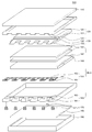
도 2는 본 발명의 일 실시예에 따른 액정 표시 장치를 설명하기 위한 액정 표시 장치의 개략적인 결합 사시도이다.
도 3은 본 발명의 일 실시예에 따른 액정 표시 장치를 설명하기 위한 개략적인 평면도이다.
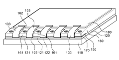
도 4는 본 발명의 일 실시예에 따른 액정 표시 장치를 설명하기 위한 도 3의 A 영역에 대한 개략적인 부분 확대 사시도이다.
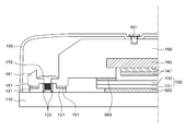
도 5는 본 발명의 일 실시예에 따른 액정 표시 장치를 설명하기 위한 도 4의 V-V'에 대한 개략적인 단면도이다.
도 6a 및 도 6b는 본 발명의 일 실시예에 따른 액정 표시 장치의 이점을 설명하기 위한 개략적인 단면도들이다.
110, 610: 커버 글래스
120, 621: 접합 부재
121: 수용부
122: 비수용부
123: 너트
130: 표시 패널
131: 상부 기판
132: 하부 기판
133: 플렉서블 인쇄 회로 기판
141: 광학 시트
142: 도광판
143: 광원부
150: 충진 부재
151: 충진 부재의 제1 부분
152: 충진 부재의 제2 부분
160, 660: 가이드 몰드
161, 661: 돌출부
162: 비돌출부
170: 스크류
171: 헤드 부분
172: 숄더 부분
173: 스크류 부분
180: 인쇄 회로 기판
190, 690: 커버 쉴드
601: 커버 스크류
602: 광학 접착제
603: 접착 테이프
651: 접착 부재
H1: 개구부
H2: 삽입 홀
Claims (12)
- 표시 패널;
상기 표시 패널 상부의 커버 글래스;
상기 커버 글래스의 일면에 배치되고, 서로 이격되어 위치하는 복수의 수용부 및 상기 복수의 수용부 사이에 위치하는 비수용부를 구비하는 접합 부재;
상기 표시 패널 하부의 도광판, 광학 시트 및 광원부를 수납하도록 구성되고, 상기 복수의 수용부에 대응하도록 측면으로부터 돌출된 복수의 돌출부를 구비하는 가이드 몰드; 및
상기 가이드 몰드의 상기 복수의 돌출부를 관통하여 상기 복수의 수용부에 체결되는 복수의 스크류를 포함하는, 액정 표시 장치. - 제1항에 있어서,
상기 가이드 몰드와 상기 접합 부재 사이에 배치된 충진 부재를 더 포함하고,
상기 충진 부재는 상기 복수의 돌출부에 대응되는 복수의 제1 부분 및 상기 복수의 제1 부분을 서로 연결하는 제2 부분을 포함하는, 액정 표시 장치. - 제2항에 있어서,
상기 복수의 제1 부분은 상기 복수의 수용부와 상기 복수의 돌출부를 접착하는 접착 물질 또는 상기 복수의 수용부와 상기 복수의 돌출부 사이의 간격을 충진하는 탄성 물질로 이루어진, 액정 표시 장치. - 제2항에 있어서,
상기 가이드 몰드 배면의 인쇄 회로 기판(Printed Circuit Board; PCB); 및
상기 표시 패널과 연결되고, 상기 인쇄 회로 기판으로부터 제공되는 신호를 상기 표시 패널로 전달하도록 구성된 플렉서블 인쇄 회로 기판(Flexible Printed Circuit Board; FPCB)을 더 포함하고,
상기 복수의 수용부의 두께는 상기 비수용부의 두께보다 크며,
상기 플렉서블 인쇄 회로 기판은 상기 접합 부재의 내측으로부터 상기 복수의 수용부 사이를 통과하여 상기 접합 부재의 외측으로 연장되는, 액정 표시 장치. - 제4항에 있어서,
상기 충진 부재의 상기 제2 부분은 상기 플렉서블 인쇄 회로 기판을 상기 접합 부재의 일면으로 밀착시키도록 상기 플렉서블 인쇄 회로 기판과 상기 가이드 몰드 사이를 충진하는 탄성 물질로 이루지는, 액정 표시 장치. - 제4항에 있어서,
상기 인쇄 회로 기판을 수용하는 커버 쉴드를 더 포함하고,
상기 커버 쉴드와 상기 가이드 몰드는 커버 스크류로 체결되는, 액정 표시 장치. - 제1항에 있어서,
상기 복수의 스크류 각각은,
상기 복수의 수용부에 삽입되는 스크류 부분;
상기 스크류 부분과 연결된 숄더(shoulder) 부분; 및
상기 숄더 부분과 연결되고, 상기 숄더 부분의 직경보다 큰 직경을 갖는 헤드(head) 부분을 포함하는, 액정 표시 장치. - 제7항에 있어서,
상기 복수의 스크류가 상기 복수의 수용부에 체결될 경우, 상기 스크류 부분의 일면은 상기 스크류 부분의 일면과 마주하는 상기 커버 글래스의 일면으로부터 이격된, 액정 표시 장치. - 제8항에 있어서,
상기 복수의 수용부 각각은 상기 스크류의 스크류 부분과 결속되는 너트를 포함하고,
상기 스크류가 상기 돌출부에 삽입되는 경우, 상기 스크류의 헤드 부분의 배면으로부터 상기 헤드 부분의 배면과 마주하는 상기 너트의 일면까지의 거리는 상기 스크류의 상기 숄더 부분의 높이보다 큰, 액정 표시 장치. - 커버 글래스;
상기 커버 글래스 하부의 표시 패널;
상기 표시 패널 하부의 백라이트 유닛; 및
상기 백라이트 유닛의 가이드 몰드를 관통하여 상기 커버 글래스의 배면에 배치된 접합 부재와 결속되도록 구성된 복수의 스크류를 포함하고,
상기 가이드 몰드는 상기 스크류가 삽입될 수 있도록 측면으로부터 돌출된 복수의 돌출부를 구비하는, 액정 표시 장치. - 제10항에 있어서,
상기 표시 패널은 상기 표시 패널에 신호들을 전달하도록 구성된 플렉서블 인쇄 회로 기판을 포함하고,
상기 표시 패널은 상기 가이드 몰드의 내측에 수납되며,
상기 플렉서블 인쇄 회로 기판은 상기 가이드 몰드의 상기 내측에서 상기 복수의 돌출부 사이를 통과하여 상기 가이드 몰드의 외측으로 연장되는, 액정 표시 장치. - 제11항에 있어서,
상기 가이드 몰드와 상기 접합 부재 사이에 배치되고, 상기 표시 패널의 상기 플렉서블 인쇄 회로 기판을 상기 커버 글래스의 일면으로 밀착 시키도록 구성된 충진 부재를 더 포함하는, 액정 표시 장치.
Priority Applications (4)
| Application Number | Priority Date | Filing Date | Title |
|---|---|---|---|
| KR1020150180525A KR102487053B1 (ko) | 2015-12-16 | 2015-12-16 | 액정 표시 장치 |
| US15/359,332 US10203533B2 (en) | 2015-12-16 | 2016-11-22 | Display device |
| CN201611127173.5A CN106886100B (zh) | 2015-12-16 | 2016-12-09 | 显示装置 |
| KR1020230001850A KR102586025B1 (ko) | 2015-12-16 | 2023-01-05 | 액정 표시 장치 |
Applications Claiming Priority (1)
| Application Number | Priority Date | Filing Date | Title |
|---|---|---|---|
| KR1020150180525A KR102487053B1 (ko) | 2015-12-16 | 2015-12-16 | 액정 표시 장치 |
Related Child Applications (1)
| Application Number | Title | Priority Date | Filing Date |
|---|---|---|---|
| KR1020230001850A Division KR102586025B1 (ko) | 2015-12-16 | 2023-01-05 | 액정 표시 장치 |
Publications (2)
| Publication Number | Publication Date |
|---|---|
| KR20170072096A true KR20170072096A (ko) | 2017-06-26 |
| KR102487053B1 KR102487053B1 (ko) | 2023-01-09 |
Family
ID=59064380
Family Applications (2)
| Application Number | Title | Priority Date | Filing Date |
|---|---|---|---|
| KR1020150180525A Active KR102487053B1 (ko) | 2015-12-16 | 2015-12-16 | 액정 표시 장치 |
| KR1020230001850A Active KR102586025B1 (ko) | 2015-12-16 | 2023-01-05 | 액정 표시 장치 |
Family Applications After (1)
| Application Number | Title | Priority Date | Filing Date |
|---|---|---|---|
| KR1020230001850A Active KR102586025B1 (ko) | 2015-12-16 | 2023-01-05 | 액정 표시 장치 |
Country Status (3)
| Country | Link |
|---|---|
| US (1) | US10203533B2 (ko) |
| KR (2) | KR102487053B1 (ko) |
| CN (1) | CN106886100B (ko) |
Cited By (1)
| Publication number | Priority date | Publication date | Assignee | Title |
|---|---|---|---|---|
| KR20240068410A (ko) * | 2022-11-10 | 2024-05-17 | 엘지디스플레이 주식회사 | 표시장치 |
Families Citing this family (12)
| Publication number | Priority date | Publication date | Assignee | Title |
|---|---|---|---|---|
| KR102528952B1 (ko) * | 2016-06-28 | 2023-05-03 | 엘지디스플레이 주식회사 | 디스플레이 장치 |
| JP2019082535A (ja) * | 2017-10-30 | 2019-05-30 | シャープ株式会社 | 表示装置 |
| JP7001434B2 (ja) * | 2017-11-10 | 2022-01-19 | シャープ株式会社 | 表示装置 |
| CN108258026B (zh) * | 2018-02-11 | 2020-09-29 | 武汉华星光电半导体显示技术有限公司 | 显示面板的绑定区结构及其制作方法、显示面板 |
| CN108470754B (zh) * | 2018-03-30 | 2020-06-09 | 京东方科技集团股份有限公司 | 一种显示装置及其制作方法 |
| CN110007518B (zh) * | 2019-04-15 | 2024-02-09 | 武汉华星光电技术有限公司 | 背光模组及显示装置 |
| WO2021005674A1 (ja) * | 2019-07-08 | 2021-01-14 | 三菱電機株式会社 | 車載表示装置 |
| CN110646991A (zh) * | 2019-09-29 | 2020-01-03 | 维沃移动通信有限公司 | 显示模组及电子设备 |
| KR102880982B1 (ko) * | 2021-12-10 | 2025-11-03 | 엘지디스플레이 주식회사 | 표시장치 |
| KR20240068408A (ko) * | 2022-11-10 | 2024-05-17 | 엘지디스플레이 주식회사 | 표시장치 |
| US12471229B2 (en) | 2023-12-19 | 2025-11-11 | Ford Global Technologies, Llc | Device with tolerance absorbing removable joint and method of assembling a device with a tolerance absorbing removable joint |
| KR102729993B1 (ko) * | 2024-01-17 | 2024-11-14 | 이씨아이 주식회사 | 차량용 디스플레이 장치 |
Citations (3)
| Publication number | Priority date | Publication date | Assignee | Title |
|---|---|---|---|---|
| JPH1090656A (ja) * | 1996-09-18 | 1998-04-10 | Canon Inc | 液晶装置 |
| KR20130095923A (ko) * | 2012-02-21 | 2013-08-29 | 삼성디스플레이 주식회사 | 표시장치 및 이의 제조방법 |
| KR101421165B1 (ko) | 2006-12-29 | 2014-07-18 | 엘지디스플레이 주식회사 | 액정표시장치의 구조 및 그 형성 방법 |
Family Cites Families (23)
| Publication number | Priority date | Publication date | Assignee | Title |
|---|---|---|---|---|
| JP3205373B2 (ja) * | 1992-03-12 | 2001-09-04 | 株式会社日立製作所 | 液晶表示装置 |
| JP3940546B2 (ja) | 1999-06-07 | 2007-07-04 | 株式会社東芝 | パターン形成方法およびパターン形成材料 |
| TW569059B (en) * | 1999-12-09 | 2004-01-01 | Samsung Electronics Co Ltd | Liquid crystal display device |
| JP3789401B2 (ja) * | 2002-06-24 | 2006-06-21 | Nec液晶テクノロジー株式会社 | 液晶モジュールおよびそれを用いた液晶モニタ |
| KR100870517B1 (ko) * | 2002-07-11 | 2008-11-26 | 엘지디스플레이 주식회사 | 액정표시장치 |
| JP5026690B2 (ja) * | 2005-11-21 | 2012-09-12 | 株式会社ジャパンディスプレイイースト | 表示装置 |
| KR101494741B1 (ko) * | 2008-06-17 | 2015-02-24 | 삼성디스플레이 주식회사 | 백라이트 어셈블리 및 이를 갖는 액정표시 장치 |
| KR101074999B1 (ko) * | 2009-04-27 | 2011-10-18 | 엘지전자 주식회사 | 디스플레이 장치 |
| JP5396335B2 (ja) | 2009-05-28 | 2014-01-22 | 株式会社半導体エネルギー研究所 | タッチパネル |
| TW201101137A (en) | 2009-06-29 | 2011-01-01 | J Touch Corp | Touch panel with matrix type tactile feedback |
| KR101575906B1 (ko) * | 2009-07-17 | 2015-12-08 | 엘지전자 주식회사 | 디스플레이 장치 |
| KR101706241B1 (ko) * | 2010-12-31 | 2017-02-27 | 엘지디스플레이 주식회사 | 평판 표시장치 및 그 조립방법 |
| KR20130015453A (ko) * | 2011-08-03 | 2013-02-14 | 엘지디스플레이 주식회사 | 백라이트 어셈블리 |
| KR20130021490A (ko) * | 2011-08-23 | 2013-03-06 | 삼성디스플레이 주식회사 | 표시 장치 |
| EP2620806B1 (en) * | 2012-01-30 | 2018-08-01 | Samsung Electronics Co., Ltd. | Display apparatus with detachable glass panel |
| US9274359B2 (en) * | 2012-06-20 | 2016-03-01 | Apple Inc. | Electronic device display chassis |
| US8848130B2 (en) * | 2012-09-26 | 2014-09-30 | Dinesh C. Mathew | Computer backlight unit (BLU) attachment to cover glass/cell |
| CN104641280B (zh) * | 2012-09-26 | 2017-03-08 | 苹果公司 | 与覆盖玻璃/单元的计算机背光源(blu)附接 |
| US20150253612A1 (en) * | 2012-09-28 | 2015-09-10 | Panasonic Intellectual Property Management Co., Ltd. | Display device |
| KR20140044600A (ko) * | 2012-10-05 | 2014-04-15 | 엘지디스플레이 주식회사 | 액정표시장치 |
| JP6168798B2 (ja) * | 2013-03-12 | 2017-07-26 | 三菱電機株式会社 | 表示装置 |
| JP6403756B2 (ja) * | 2014-03-19 | 2018-10-10 | シャープ株式会社 | 照明装置及び表示装置 |
| CN104820305B (zh) * | 2015-05-19 | 2018-12-11 | 深圳市华星光电技术有限公司 | 显示装置 |
-
2015
- 2015-12-16 KR KR1020150180525A patent/KR102487053B1/ko active Active
-
2016
- 2016-11-22 US US15/359,332 patent/US10203533B2/en active Active
- 2016-12-09 CN CN201611127173.5A patent/CN106886100B/zh active Active
-
2023
- 2023-01-05 KR KR1020230001850A patent/KR102586025B1/ko active Active
Patent Citations (3)
| Publication number | Priority date | Publication date | Assignee | Title |
|---|---|---|---|---|
| JPH1090656A (ja) * | 1996-09-18 | 1998-04-10 | Canon Inc | 液晶装置 |
| KR101421165B1 (ko) | 2006-12-29 | 2014-07-18 | 엘지디스플레이 주식회사 | 액정표시장치의 구조 및 그 형성 방법 |
| KR20130095923A (ko) * | 2012-02-21 | 2013-08-29 | 삼성디스플레이 주식회사 | 표시장치 및 이의 제조방법 |
Cited By (1)
| Publication number | Priority date | Publication date | Assignee | Title |
|---|---|---|---|---|
| KR20240068410A (ko) * | 2022-11-10 | 2024-05-17 | 엘지디스플레이 주식회사 | 표시장치 |
Also Published As
| Publication number | Publication date |
|---|---|
| KR20230008906A (ko) | 2023-01-16 |
| US10203533B2 (en) | 2019-02-12 |
| CN106886100B (zh) | 2020-10-13 |
| KR102487053B1 (ko) | 2023-01-09 |
| KR102586025B1 (ko) | 2023-10-05 |
| US20170176806A1 (en) | 2017-06-22 |
| CN106886100A (zh) | 2017-06-23 |
Similar Documents
| Publication | Publication Date | Title |
|---|---|---|
| KR102586025B1 (ko) | 액정 표시 장치 | |
| US10007151B2 (en) | Display panel and display device including the same | |
| US9436309B2 (en) | Liquid crystal display device integrated with touch screen panel | |
| US20090174996A1 (en) | Display device | |
| US20070132909A1 (en) | Liquid crystal display device | |
| US20100302478A1 (en) | Liquid crystal display device | |
| US7796214B2 (en) | Liquid crystal display having flexible printed circuit sandwiched between liquid crystal panel and light guide plate thereof | |
| KR102311058B1 (ko) | 표시 장치 | |
| US20170293176A1 (en) | Display panel and display apparatus including the same | |
| JP2008225414A (ja) | 液晶表示パネル | |
| KR20180031860A (ko) | 표시 장치 | |
| CN103075676B (zh) | 背光单元及其制造方法和包括该背光单元的液晶显示装置 | |
| JP2008293979A (ja) | 光源モジュールとバックライトアセンブリ及びこれらを有する表示装置並びにバックライトアセンブリの厚さを減少させる方法 | |
| KR101834350B1 (ko) | 디스플레이 장치 | |
| KR20190090897A (ko) | 표시 장치 | |
| US7999884B2 (en) | Liquid crystal display | |
| KR101463683B1 (ko) | 액정표시장치 | |
| KR101937743B1 (ko) | 백라이트 유닛 및 이를 구비한 액정표시장치 | |
| KR101898588B1 (ko) | 디스플레이 장치 | |
| JP2009192769A (ja) | 液晶表示装置 | |
| US20140078413A1 (en) | Liquid crystal display structure | |
| JP2008203728A (ja) | 液晶表示装置 | |
| KR20170079244A (ko) | 액정 표시 장치 | |
| KR20170080791A (ko) | 액정표시장치를 구비한 전자기기 | |
| KR102523535B1 (ko) | 표시장치 |
Legal Events
| Date | Code | Title | Description |
|---|---|---|---|
| PA0109 | Patent application |
St.27 status event code: A-0-1-A10-A12-nap-PA0109 |
|
| R17-X000 | Change to representative recorded |
St.27 status event code: A-3-3-R10-R17-oth-X000 |
|
| PG1501 | Laying open of application |
St.27 status event code: A-1-1-Q10-Q12-nap-PG1501 |
|
| P22-X000 | Classification modified |
St.27 status event code: A-2-2-P10-P22-nap-X000 |
|
| A201 | Request for examination | ||
| PA0201 | Request for examination |
St.27 status event code: A-1-2-D10-D11-exm-PA0201 |
|
| D13-X000 | Search requested |
St.27 status event code: A-1-2-D10-D13-srh-X000 |
|
| D14-X000 | Search report completed |
St.27 status event code: A-1-2-D10-D14-srh-X000 |
|
| E902 | Notification of reason for refusal | ||
| PE0902 | Notice of grounds for rejection |
St.27 status event code: A-1-2-D10-D21-exm-PE0902 |
|
| E13-X000 | Pre-grant limitation requested |
St.27 status event code: A-2-3-E10-E13-lim-X000 |
|
| P11-X000 | Amendment of application requested |
St.27 status event code: A-2-2-P10-P11-nap-X000 |
|
| P13-X000 | Application amended |
St.27 status event code: A-2-2-P10-P13-nap-X000 |
|
| E701 | Decision to grant or registration of patent right | ||
| PE0701 | Decision of registration |
St.27 status event code: A-1-2-D10-D22-exm-PE0701 |
|
| A107 | Divisional application of patent | ||
| GRNT | Written decision to grant | ||
| PA0107 | Divisional application |
St.27 status event code: A-0-1-A10-A18-div-PA0107 St.27 status event code: A-0-1-A10-A16-div-PA0107 |
|
| PR0701 | Registration of establishment |
St.27 status event code: A-2-4-F10-F11-exm-PR0701 |
|
| PR1002 | Payment of registration fee |
St.27 status event code: A-2-2-U10-U11-oth-PR1002 Fee payment year number: 1 |
|
| PG1601 | Publication of registration |
St.27 status event code: A-4-4-Q10-Q13-nap-PG1601 |
|
| PR1001 | Payment of annual fee |
St.27 status event code: A-4-4-U10-U11-oth-PR1001 Fee payment year number: 4 |
|
| U11 | Full renewal or maintenance fee paid |
Free format text: ST27 STATUS EVENT CODE: A-4-4-U10-U11-OTH-PR1001 (AS PROVIDED BY THE NATIONAL OFFICE) Year of fee payment: 4 |