KR20170076571A - 성막 장치 - Google Patents
성막 장치 Download PDFInfo
- Publication number
- KR20170076571A KR20170076571A KR1020160173470A KR20160173470A KR20170076571A KR 20170076571 A KR20170076571 A KR 20170076571A KR 1020160173470 A KR1020160173470 A KR 1020160173470A KR 20160173470 A KR20160173470 A KR 20160173470A KR 20170076571 A KR20170076571 A KR 20170076571A
- Authority
- KR
- South Korea
- Prior art keywords
- gas
- region
- rotary table
- reaction gas
- wafer
- Prior art date
- Legal status (The legal status is an assumption and is not a legal conclusion. Google has not performed a legal analysis and makes no representation as to the accuracy of the status listed.)
- Granted
Links
Images


Classifications
-
- C—CHEMISTRY; METALLURGY
- C23—COATING METALLIC MATERIAL; COATING MATERIAL WITH METALLIC MATERIAL; CHEMICAL SURFACE TREATMENT; DIFFUSION TREATMENT OF METALLIC MATERIAL; COATING BY VACUUM EVAPORATION, BY SPUTTERING, BY ION IMPLANTATION OR BY CHEMICAL VAPOUR DEPOSITION, IN GENERAL; INHIBITING CORROSION OF METALLIC MATERIAL OR INCRUSTATION IN GENERAL
- C23C—COATING METALLIC MATERIAL; COATING MATERIAL WITH METALLIC MATERIAL; SURFACE TREATMENT OF METALLIC MATERIAL BY DIFFUSION INTO THE SURFACE, BY CHEMICAL CONVERSION OR SUBSTITUTION; COATING BY VACUUM EVAPORATION, BY SPUTTERING, BY ION IMPLANTATION OR BY CHEMICAL VAPOUR DEPOSITION, IN GENERAL
- C23C16/00—Chemical coating by decomposition of gaseous compounds, without leaving reaction products of surface material in the coating, i.e. chemical vapour deposition [CVD] processes
- C23C16/44—Chemical coating by decomposition of gaseous compounds, without leaving reaction products of surface material in the coating, i.e. chemical vapour deposition [CVD] processes characterised by the method of coating
- C23C16/50—Chemical coating by decomposition of gaseous compounds, without leaving reaction products of surface material in the coating, i.e. chemical vapour deposition [CVD] processes characterised by the method of coating using electric discharges
- C23C16/511—Chemical coating by decomposition of gaseous compounds, without leaving reaction products of surface material in the coating, i.e. chemical vapour deposition [CVD] processes characterised by the method of coating using electric discharges using microwave discharges
-
- H01L21/02274—
-
- C—CHEMISTRY; METALLURGY
- C23—COATING METALLIC MATERIAL; COATING MATERIAL WITH METALLIC MATERIAL; CHEMICAL SURFACE TREATMENT; DIFFUSION TREATMENT OF METALLIC MATERIAL; COATING BY VACUUM EVAPORATION, BY SPUTTERING, BY ION IMPLANTATION OR BY CHEMICAL VAPOUR DEPOSITION, IN GENERAL; INHIBITING CORROSION OF METALLIC MATERIAL OR INCRUSTATION IN GENERAL
- C23C—COATING METALLIC MATERIAL; COATING MATERIAL WITH METALLIC MATERIAL; SURFACE TREATMENT OF METALLIC MATERIAL BY DIFFUSION INTO THE SURFACE, BY CHEMICAL CONVERSION OR SUBSTITUTION; COATING BY VACUUM EVAPORATION, BY SPUTTERING, BY ION IMPLANTATION OR BY CHEMICAL VAPOUR DEPOSITION, IN GENERAL
- C23C16/00—Chemical coating by decomposition of gaseous compounds, without leaving reaction products of surface material in the coating, i.e. chemical vapour deposition [CVD] processes
- C23C16/44—Chemical coating by decomposition of gaseous compounds, without leaving reaction products of surface material in the coating, i.e. chemical vapour deposition [CVD] processes characterised by the method of coating
- C23C16/4412—Details relating to the exhausts, e.g. pumps, filters, scrubbers, particle traps
-
- C—CHEMISTRY; METALLURGY
- C23—COATING METALLIC MATERIAL; COATING MATERIAL WITH METALLIC MATERIAL; CHEMICAL SURFACE TREATMENT; DIFFUSION TREATMENT OF METALLIC MATERIAL; COATING BY VACUUM EVAPORATION, BY SPUTTERING, BY ION IMPLANTATION OR BY CHEMICAL VAPOUR DEPOSITION, IN GENERAL; INHIBITING CORROSION OF METALLIC MATERIAL OR INCRUSTATION IN GENERAL
- C23C—COATING METALLIC MATERIAL; COATING MATERIAL WITH METALLIC MATERIAL; SURFACE TREATMENT OF METALLIC MATERIAL BY DIFFUSION INTO THE SURFACE, BY CHEMICAL CONVERSION OR SUBSTITUTION; COATING BY VACUUM EVAPORATION, BY SPUTTERING, BY ION IMPLANTATION OR BY CHEMICAL VAPOUR DEPOSITION, IN GENERAL
- C23C16/00—Chemical coating by decomposition of gaseous compounds, without leaving reaction products of surface material in the coating, i.e. chemical vapour deposition [CVD] processes
- C23C16/44—Chemical coating by decomposition of gaseous compounds, without leaving reaction products of surface material in the coating, i.e. chemical vapour deposition [CVD] processes characterised by the method of coating
- C23C16/455—Chemical coating by decomposition of gaseous compounds, without leaving reaction products of surface material in the coating, i.e. chemical vapour deposition [CVD] processes characterised by the method of coating characterised by the method used for introducing gases into reaction chamber or for modifying gas flows in reaction chamber
- C23C16/45523—Pulsed gas flow or change of composition over time
- C23C16/45525—Atomic layer deposition [ALD]
- C23C16/45544—Atomic layer deposition [ALD] characterized by the apparatus
- C23C16/45548—Atomic layer deposition [ALD] characterized by the apparatus having arrangements for gas injection at different locations of the reactor for each ALD half-reaction
- C23C16/45551—Atomic layer deposition [ALD] characterized by the apparatus having arrangements for gas injection at different locations of the reactor for each ALD half-reaction for relative movement of the substrate and the gas injectors or half-reaction reactor compartments
-
- C—CHEMISTRY; METALLURGY
- C23—COATING METALLIC MATERIAL; COATING MATERIAL WITH METALLIC MATERIAL; CHEMICAL SURFACE TREATMENT; DIFFUSION TREATMENT OF METALLIC MATERIAL; COATING BY VACUUM EVAPORATION, BY SPUTTERING, BY ION IMPLANTATION OR BY CHEMICAL VAPOUR DEPOSITION, IN GENERAL; INHIBITING CORROSION OF METALLIC MATERIAL OR INCRUSTATION IN GENERAL
- C23C—COATING METALLIC MATERIAL; COATING MATERIAL WITH METALLIC MATERIAL; SURFACE TREATMENT OF METALLIC MATERIAL BY DIFFUSION INTO THE SURFACE, BY CHEMICAL CONVERSION OR SUBSTITUTION; COATING BY VACUUM EVAPORATION, BY SPUTTERING, BY ION IMPLANTATION OR BY CHEMICAL VAPOUR DEPOSITION, IN GENERAL
- C23C16/00—Chemical coating by decomposition of gaseous compounds, without leaving reaction products of surface material in the coating, i.e. chemical vapour deposition [CVD] processes
- C23C16/44—Chemical coating by decomposition of gaseous compounds, without leaving reaction products of surface material in the coating, i.e. chemical vapour deposition [CVD] processes characterised by the method of coating
- C23C16/455—Chemical coating by decomposition of gaseous compounds, without leaving reaction products of surface material in the coating, i.e. chemical vapour deposition [CVD] processes characterised by the method of coating characterised by the method used for introducing gases into reaction chamber or for modifying gas flows in reaction chamber
- C23C16/45563—Gas nozzles
- C23C16/45578—Elongated nozzles, tubes with holes
-
- C—CHEMISTRY; METALLURGY
- C23—COATING METALLIC MATERIAL; COATING MATERIAL WITH METALLIC MATERIAL; CHEMICAL SURFACE TREATMENT; DIFFUSION TREATMENT OF METALLIC MATERIAL; COATING BY VACUUM EVAPORATION, BY SPUTTERING, BY ION IMPLANTATION OR BY CHEMICAL VAPOUR DEPOSITION, IN GENERAL; INHIBITING CORROSION OF METALLIC MATERIAL OR INCRUSTATION IN GENERAL
- C23C—COATING METALLIC MATERIAL; COATING MATERIAL WITH METALLIC MATERIAL; SURFACE TREATMENT OF METALLIC MATERIAL BY DIFFUSION INTO THE SURFACE, BY CHEMICAL CONVERSION OR SUBSTITUTION; COATING BY VACUUM EVAPORATION, BY SPUTTERING, BY ION IMPLANTATION OR BY CHEMICAL VAPOUR DEPOSITION, IN GENERAL
- C23C16/00—Chemical coating by decomposition of gaseous compounds, without leaving reaction products of surface material in the coating, i.e. chemical vapour deposition [CVD] processes
- C23C16/44—Chemical coating by decomposition of gaseous compounds, without leaving reaction products of surface material in the coating, i.e. chemical vapour deposition [CVD] processes characterised by the method of coating
- C23C16/458—Chemical coating by decomposition of gaseous compounds, without leaving reaction products of surface material in the coating, i.e. chemical vapour deposition [CVD] processes characterised by the method of coating characterised by the method used for supporting substrates in the reaction chamber
- C23C16/4582—Rigid and flat substrates, e.g. plates or discs
- C23C16/4583—Rigid and flat substrates, e.g. plates or discs the substrate being supported substantially horizontally
- C23C16/4584—Rigid and flat substrates, e.g. plates or discs the substrate being supported substantially horizontally the substrate being rotated
-
- H01L21/0228—
-
- H01L21/02315—
-
- H01L21/205—
-
- H01L21/68742—
-
- H—ELECTRICITY
- H10—SEMICONDUCTOR DEVICES; ELECTRIC SOLID-STATE DEVICES NOT OTHERWISE PROVIDED FOR
- H10P—GENERIC PROCESSES OR APPARATUS FOR THE MANUFACTURE OR TREATMENT OF DEVICES COVERED BY CLASS H10
- H10P14/00—Formation of materials, e.g. in the shape of layers or pillars
- H10P14/60—Formation of materials, e.g. in the shape of layers or pillars of insulating materials
- H10P14/63—Formation of materials, e.g. in the shape of layers or pillars of insulating materials characterised by the formation processes
- H10P14/6326—Deposition processes
- H10P14/6328—Deposition from the gas or vapour phase
- H10P14/6334—Deposition from the gas or vapour phase using decomposition or reaction of gaseous or vapour phase compounds, i.e. chemical vapour deposition
- H10P14/6336—Deposition from the gas or vapour phase using decomposition or reaction of gaseous or vapour phase compounds, i.e. chemical vapour deposition in the presence of a plasma [PECVD]
-
- H—ELECTRICITY
- H10—SEMICONDUCTOR DEVICES; ELECTRIC SOLID-STATE DEVICES NOT OTHERWISE PROVIDED FOR
- H10P—GENERIC PROCESSES OR APPARATUS FOR THE MANUFACTURE OR TREATMENT OF DEVICES COVERED BY CLASS H10
- H10P14/00—Formation of materials, e.g. in the shape of layers or pillars
- H10P14/60—Formation of materials, e.g. in the shape of layers or pillars of insulating materials
- H10P14/63—Formation of materials, e.g. in the shape of layers or pillars of insulating materials characterised by the formation processes
- H10P14/6326—Deposition processes
- H10P14/6328—Deposition from the gas or vapour phase
- H10P14/6334—Deposition from the gas or vapour phase using decomposition or reaction of gaseous or vapour phase compounds, i.e. chemical vapour deposition
- H10P14/6339—Deposition from the gas or vapour phase using decomposition or reaction of gaseous or vapour phase compounds, i.e. chemical vapour deposition deposition by cyclic CVD, e.g. ALD, ALE or pulsed CVD
-
- H—ELECTRICITY
- H10—SEMICONDUCTOR DEVICES; ELECTRIC SOLID-STATE DEVICES NOT OTHERWISE PROVIDED FOR
- H10P—GENERIC PROCESSES OR APPARATUS FOR THE MANUFACTURE OR TREATMENT OF DEVICES COVERED BY CLASS H10
- H10P14/00—Formation of materials, e.g. in the shape of layers or pillars
- H10P14/60—Formation of materials, e.g. in the shape of layers or pillars of insulating materials
- H10P14/66—Formation of materials, e.g. in the shape of layers or pillars of insulating materials characterised by the type of materials
- H10P14/668—Formation of materials, e.g. in the shape of layers or pillars of insulating materials characterised by the type of materials the materials being characterised by the deposition precursor materials
- H10P14/6681—Formation of materials, e.g. in the shape of layers or pillars of insulating materials characterised by the type of materials the materials being characterised by the deposition precursor materials the precursor containing a compound comprising Si
- H10P14/6682—Formation of materials, e.g. in the shape of layers or pillars of insulating materials characterised by the type of materials the materials being characterised by the deposition precursor materials the precursor containing a compound comprising Si the compound being a silane, e.g. disilane, methylsilane or chlorosilane
-
- H—ELECTRICITY
- H10—SEMICONDUCTOR DEVICES; ELECTRIC SOLID-STATE DEVICES NOT OTHERWISE PROVIDED FOR
- H10P—GENERIC PROCESSES OR APPARATUS FOR THE MANUFACTURE OR TREATMENT OF DEVICES COVERED BY CLASS H10
- H10P14/00—Formation of materials, e.g. in the shape of layers or pillars
- H10P14/60—Formation of materials, e.g. in the shape of layers or pillars of insulating materials
- H10P14/69—Inorganic materials
- H10P14/694—Inorganic materials composed of nitrides
- H10P14/6943—Inorganic materials composed of nitrides containing silicon
- H10P14/69433—Inorganic materials composed of nitrides containing silicon the material being a silicon nitride not containing oxygen, e.g. SixNy or SixByNz
-
- H—ELECTRICITY
- H10—SEMICONDUCTOR DEVICES; ELECTRIC SOLID-STATE DEVICES NOT OTHERWISE PROVIDED FOR
- H10P—GENERIC PROCESSES OR APPARATUS FOR THE MANUFACTURE OR TREATMENT OF DEVICES COVERED BY CLASS H10
- H10P72/00—Handling or holding of wafers, substrates or devices during manufacture or treatment thereof
- H10P72/70—Handling or holding of wafers, substrates or devices during manufacture or treatment thereof for supporting or gripping
- H10P72/76—Handling or holding of wafers, substrates or devices during manufacture or treatment thereof for supporting or gripping using mechanical means, e.g. clamps or pinches
- H10P72/7604—Handling or holding of wafers, substrates or devices during manufacture or treatment thereof for supporting or gripping using mechanical means, e.g. clamps or pinches the wafers being placed on a susceptor, stage or support
- H10P72/7612—Handling or holding of wafers, substrates or devices during manufacture or treatment thereof for supporting or gripping using mechanical means, e.g. clamps or pinches the wafers being placed on a susceptor, stage or support characterised by lifting arrangements, e.g. lift pins
-
- H—ELECTRICITY
- H10—SEMICONDUCTOR DEVICES; ELECTRIC SOLID-STATE DEVICES NOT OTHERWISE PROVIDED FOR
- H10P—GENERIC PROCESSES OR APPARATUS FOR THE MANUFACTURE OR TREATMENT OF DEVICES COVERED BY CLASS H10
- H10P72/00—Handling or holding of wafers, substrates or devices during manufacture or treatment thereof
- H10P72/70—Handling or holding of wafers, substrates or devices during manufacture or treatment thereof for supporting or gripping
- H10P72/76—Handling or holding of wafers, substrates or devices during manufacture or treatment thereof for supporting or gripping using mechanical means, e.g. clamps or pinches
- H10P72/7604—Handling or holding of wafers, substrates or devices during manufacture or treatment thereof for supporting or gripping using mechanical means, e.g. clamps or pinches the wafers being placed on a susceptor, stage or support
- H10P72/7618—Handling or holding of wafers, substrates or devices during manufacture or treatment thereof for supporting or gripping using mechanical means, e.g. clamps or pinches the wafers being placed on a susceptor, stage or support characterised by a movable susceptor, stage or support, others than those only rotating on their own vertical axis, e.g. susceptors on a rotating carrousel
-
- H—ELECTRICITY
- H10—SEMICONDUCTOR DEVICES; ELECTRIC SOLID-STATE DEVICES NOT OTHERWISE PROVIDED FOR
- H10P—GENERIC PROCESSES OR APPARATUS FOR THE MANUFACTURE OR TREATMENT OF DEVICES COVERED BY CLASS H10
- H10P72/00—Handling or holding of wafers, substrates or devices during manufacture or treatment thereof
- H10P72/70—Handling or holding of wafers, substrates or devices during manufacture or treatment thereof for supporting or gripping
- H10P72/76—Handling or holding of wafers, substrates or devices during manufacture or treatment thereof for supporting or gripping using mechanical means, e.g. clamps or pinches
- H10P72/7604—Handling or holding of wafers, substrates or devices during manufacture or treatment thereof for supporting or gripping using mechanical means, e.g. clamps or pinches the wafers being placed on a susceptor, stage or support
- H10P72/7621—Handling or holding of wafers, substrates or devices during manufacture or treatment thereof for supporting or gripping using mechanical means, e.g. clamps or pinches the wafers being placed on a susceptor, stage or support characterised by supporting two or more semiconductor substrates
Landscapes
- Chemical & Material Sciences (AREA)
- Engineering & Computer Science (AREA)
- General Chemical & Material Sciences (AREA)
- Chemical Kinetics & Catalysis (AREA)
- Materials Engineering (AREA)
- Mechanical Engineering (AREA)
- Metallurgy (AREA)
- Organic Chemistry (AREA)
- Physics & Mathematics (AREA)
- Plasma & Fusion (AREA)
- Chemical Vapour Deposition (AREA)
- Plasma Technology (AREA)
Abstract
Description
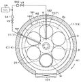
도 2는 상기 성막 장치의 횡단 평면도이다.
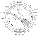
도 3은 상기 성막 장치를 상면측에서 본 평면도이다.
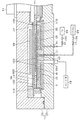
도 4는 상기 성막 장치에 형성되어 있는 제1 영역의 확대 종단 측면도이다.
도 5는 상기 제1 영역에 설치되어 있는 원료 가스 유닛을 하면측에서 본 평면도이다.
도 6은 상기 성막 장치에 설치되어 있는 제2 영역의 확대 종단 측면도이다.
도 7은 상기 제2 영역에 설치되어 있는 가스 인젝터의 배치 상태를 도시하는 모식도이다.
도 8은 상기 제2 영역에 설치되어 있는 플라즈마 형성부 내의 슬롯판의 평면도이다.
도 9는 상기 성막 장치의 작용을 도시하는 설명도이다.
도 10은 변형예에 관한 성막 장치의 설명도이다.
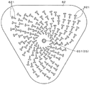
도 11은 실시예에 관한 막 두께 분포를 도시하는 설명도이다.
도 12는 비교예에 관한 막 두께 분포를 도시하는 설명도이다.
W : 웨이퍼 2 : 회전 테이블
21 : 기판 적재 영역 330 : 토출부
6 : 플라즈마 형성부 7 : 가스 인젝터
8 : 제어부
Claims (5)
- 진공 용기 내에서 기판에 박막을 성막하기 위한 성막 장치에 있어서,
상기 진공 용기 내에 설치되고, 기판이 적재되는 기판 적재 영역을 회전 중심 둘레로 공전시키기 위한 회전 테이블과,
상기 기판 적재 영역이 통과하는 공전면을, 상기 기판 적재 영역의 공전 방향과 교차하는 방향으로 구획해서 이루어지는 제1 영역에, 상기 회전 테이블과 대향하도록 설치된 토출부로부터 상기 박막의 원료 가스를 공급하는 제1 가스 공급부와,
상기 토출부의 주위를 둘러싸는 제1 폐로를 따라 연장되도록 형성된 배기구로부터 배기를 행하는 배기부와,
상기 배기구의 주위를 둘러싸는 제2 폐로를 따라 연장되도록 형성된 분리 가스 공급구로부터, 상기 제2 폐로의 내외를 분리하기 위한 분리 가스를 공급하는 제2 가스 공급부와,
상기 기판 적재 영역의 공전 방향과 교차하는 방향으로 신장되고, 상기 제2 폐로의 외측에 형성된 제2 영역을 사이에 두어 간격을 두고 배치됨과 함께, 각각, 상기 원료 가스와 반응하는 반응 가스를 제2 영역측을 향해서 토출하기 위한 가스 토출 구멍이 형성된 2개의 가스 인젝터를 구비한 제3 가스 공급부와,
상기 제2 영역을 향해서 토출된 반응 가스를 플라즈마화하기 위한 플라즈마 형성부를 포함하고,
상기 2개의 가스 인젝터가 이루는 각도가 180도 미만인 성막 장치. - 제1항에 있어서,
상기 진공 용기에는, 회전 테이블의 주연측으로부터, 상기 제2 영역을 향해서 상기 반응 가스를 토출하는 가스 토출 구멍을 구비한 제4 가스 공급부가 더 설치되어 있는, 성막 장치. - 제1항에 있어서,
상기 제2 영역보다도 회전 테이블의 외측의 위치이며, 상기 진공 용기와 회전 테이블과의 사이에 개구되어, 상기 반응 가스의 배기를 행하는 배기구를 구비한 반응 가스 배기부를 더 포함하는, 성막 장치. - 제1항에 있어서,
상기 플라즈마 형성부는, 상기 제2 영역의 평면 형상에 대응하는 영역 내에, 마이크로파를 방사하기 위한 다수의 슬롯이 형성된 슬롯판과, 상기 회전 테이블과 슬롯판과의 사이에 설치되어, 상기 슬롯판으로부터 방사되는 마이크로파가 투과하는 유전체 플레이트를 포함하는, 성막 장치. - 제1항 내지 제4항 중 어느 한 항에 있어서,
상기 제1 영역은, 기판 적재 영역의 공전 방향과 교차하는 방향으로 신장되고, 간격을 두고 배치된 2변을 갖고, 상기 2변이 이루는 각도가 180도 미만인, 성막 장치.
Applications Claiming Priority (2)
| Application Number | Priority Date | Filing Date | Title |
|---|---|---|---|
| JP2015252081A JP6569521B2 (ja) | 2015-12-24 | 2015-12-24 | 成膜装置 |
| JPJP-P-2015-252081 | 2015-12-24 |
Publications (2)
| Publication Number | Publication Date |
|---|---|
| KR20170076571A true KR20170076571A (ko) | 2017-07-04 |
| KR102062948B1 KR102062948B1 (ko) | 2020-01-06 |
Family
ID=59087019
Family Applications (1)
| Application Number | Title | Priority Date | Filing Date |
|---|---|---|---|
| KR1020160173470A Active KR102062948B1 (ko) | 2015-12-24 | 2016-12-19 | 성막 장치 |
Country Status (3)
| Country | Link |
|---|---|
| US (1) | US10519550B2 (ko) |
| JP (1) | JP6569521B2 (ko) |
| KR (1) | KR102062948B1 (ko) |
Families Citing this family (7)
| Publication number | Priority date | Publication date | Assignee | Title |
|---|---|---|---|---|
| JP6134191B2 (ja) * | 2013-04-07 | 2017-05-24 | 村川 惠美 | 回転型セミバッチald装置 |
| JP6305314B2 (ja) * | 2014-10-29 | 2018-04-04 | 東京エレクトロン株式会社 | 成膜装置およびシャワーヘッド |
| KR102638572B1 (ko) * | 2015-06-17 | 2024-02-21 | 어플라이드 머티어리얼스, 인코포레이티드 | 프로세스 챔버 내의 가스 제어 |
| JP6930382B2 (ja) | 2017-11-06 | 2021-09-01 | 東京エレクトロン株式会社 | 成膜装置及び成膜方法 |
| JP7238350B2 (ja) | 2018-11-12 | 2023-03-14 | 東京エレクトロン株式会社 | 成膜装置及び成膜方法 |
| JP6894482B2 (ja) * | 2019-09-12 | 2021-06-30 | 株式会社Kokusai Electric | 基板処理装置、半導体装置の製造方法、プログラム及び記録媒体 |
| FI130143B (en) * | 2020-10-12 | 2023-03-10 | Beneq Oy | Apparatus and method for atomic layer growing |
Family Cites Families (11)
| Publication number | Priority date | Publication date | Assignee | Title |
|---|---|---|---|---|
| JP2006524914A (ja) * | 2003-03-31 | 2006-11-02 | 東京エレクトロン株式会社 | プラズマ処理システム及び方法 |
| JP5423205B2 (ja) | 2008-08-29 | 2014-02-19 | 東京エレクトロン株式会社 | 成膜装置 |
| JP5299241B2 (ja) * | 2008-11-28 | 2013-09-25 | 株式会社島津製作所 | パーティクル計数装置 |
| JP5141607B2 (ja) | 2009-03-13 | 2013-02-13 | 東京エレクトロン株式会社 | 成膜装置 |
| JP5327147B2 (ja) * | 2009-12-25 | 2013-10-30 | 東京エレクトロン株式会社 | プラズマ処理装置 |
| JP5882777B2 (ja) * | 2012-02-14 | 2016-03-09 | 東京エレクトロン株式会社 | 成膜装置 |
| JP5947138B2 (ja) * | 2012-07-25 | 2016-07-06 | 東京エレクトロン株式会社 | 成膜装置 |
| JP5839606B2 (ja) | 2013-02-26 | 2016-01-06 | 東京エレクトロン株式会社 | 窒化膜を形成する方法 |
| CN105051252B (zh) * | 2013-03-15 | 2017-11-24 | 东丽株式会社 | 等离子体cvd装置及等离子体cvd方法 |
| JP6134191B2 (ja) * | 2013-04-07 | 2017-05-24 | 村川 惠美 | 回転型セミバッチald装置 |
| JP6383674B2 (ja) * | 2014-02-19 | 2018-08-29 | 東京エレクトロン株式会社 | 基板処理装置 |
-
2015
- 2015-12-24 JP JP2015252081A patent/JP6569521B2/ja active Active
-
2016
- 2016-12-19 KR KR1020160173470A patent/KR102062948B1/ko active Active
- 2016-12-21 US US15/387,043 patent/US10519550B2/en active Active
Also Published As
| Publication number | Publication date |
|---|---|
| US20170183779A1 (en) | 2017-06-29 |
| JP6569521B2 (ja) | 2019-09-04 |
| US10519550B2 (en) | 2019-12-31 |
| JP2017117943A (ja) | 2017-06-29 |
| KR102062948B1 (ko) | 2020-01-06 |
Similar Documents
| Publication | Publication Date | Title |
|---|---|---|
| US10550467B2 (en) | Film formation apparatus | |
| KR20170076571A (ko) | 성막 장치 | |
| JP5423205B2 (ja) | 成膜装置 | |
| US10900121B2 (en) | Method of manufacturing semiconductor device and apparatus of manufacturing semiconductor device | |
| US20140023794A1 (en) | Method And Apparatus For Low Temperature ALD Deposition | |
| KR101582720B1 (ko) | 성막 장치 및 성막 방법 | |
| KR102360006B1 (ko) | 성막 장치 및 성막 방법 | |
| KR20170113155A (ko) | 플라즈마 처리 장치 및 플라즈마 처리 방법 | |
| JP2017139451A (ja) | 窒化膜の形成方法 | |
| TWI702304B (zh) | 矽氮化膜之成膜方法及成膜裝置 | |
| US20180051374A1 (en) | Film-forming apparatus, film-forming method, and storage medium | |
| JP5549754B2 (ja) | 成膜装置 | |
| KR20170102810A (ko) | 성막 방법 | |
| US10151029B2 (en) | Silicon nitride film forming method and silicon nitride film forming apparatus | |
| US9922820B2 (en) | Film forming method and film forming apparatus | |
| JP7253972B2 (ja) | 基板処理装置 | |
| KR20180054448A (ko) | 성막 장치 | |
| JP7666234B2 (ja) | 基板に成膜処理を行う装置、及び基板に成膜処理を行う装置から処理ガスを排気する方法 | |
| US20170218517A1 (en) | Method of forming nitride film | |
| JP6904150B2 (ja) | プラズマ処理装置 |
Legal Events
| Date | Code | Title | Description |
|---|---|---|---|
| PA0109 | Patent application |
St.27 status event code: A-0-1-A10-A12-nap-PA0109 |
|
| PG1501 | Laying open of application |
St.27 status event code: A-1-1-Q10-Q12-nap-PG1501 |
|
| A201 | Request for examination | ||
| PA0201 | Request for examination |
St.27 status event code: A-1-2-D10-D11-exm-PA0201 |
|
| D13-X000 | Search requested |
St.27 status event code: A-1-2-D10-D13-srh-X000 |
|
| D14-X000 | Search report completed |
St.27 status event code: A-1-2-D10-D14-srh-X000 |
|
| E902 | Notification of reason for refusal | ||
| PE0902 | Notice of grounds for rejection |
St.27 status event code: A-1-2-D10-D21-exm-PE0902 |
|
| E13-X000 | Pre-grant limitation requested |
St.27 status event code: A-2-3-E10-E13-lim-X000 |
|
| P11-X000 | Amendment of application requested |
St.27 status event code: A-2-2-P10-P11-nap-X000 |
|
| P13-X000 | Application amended |
St.27 status event code: A-2-2-P10-P13-nap-X000 |
|
| E701 | Decision to grant or registration of patent right | ||
| PE0701 | Decision of registration |
St.27 status event code: A-1-2-D10-D22-exm-PE0701 |
|
| GRNT | Written decision to grant | ||
| PR0701 | Registration of establishment |
St.27 status event code: A-2-4-F10-F11-exm-PR0701 |
|
| PR1002 | Payment of registration fee |
St.27 status event code: A-2-2-U10-U11-oth-PR1002 Fee payment year number: 1 |
|
| PG1601 | Publication of registration |
St.27 status event code: A-4-4-Q10-Q13-nap-PG1601 |
|
| FPAY | Annual fee payment |
Payment date: 20221202 Year of fee payment: 4 |
|
| PR1001 | Payment of annual fee |
St.27 status event code: A-4-4-U10-U11-oth-PR1001 Fee payment year number: 4 |
|
| PR1001 | Payment of annual fee |
St.27 status event code: A-4-4-U10-U11-oth-PR1001 Fee payment year number: 5 |
|
| P22-X000 | Classification modified |
St.27 status event code: A-4-4-P10-P22-nap-X000 |
|
| PR1001 | Payment of annual fee |
St.27 status event code: A-4-4-U10-U11-oth-PR1001 Fee payment year number: 6 |
|
| P22-X000 | Classification modified |
St.27 status event code: A-4-4-P10-P22-nap-X000 |