KR20170077013A - Substrate processing apparatus, method of manufacturing semiconductor device, and recording medium - Google Patents
Substrate processing apparatus, method of manufacturing semiconductor device, and recording medium Download PDFInfo
- Publication number
- KR20170077013A KR20170077013A KR1020160032170A KR20160032170A KR20170077013A KR 20170077013 A KR20170077013 A KR 20170077013A KR 1020160032170 A KR1020160032170 A KR 1020160032170A KR 20160032170 A KR20160032170 A KR 20160032170A KR 20170077013 A KR20170077013 A KR 20170077013A
- Authority
- KR
- South Korea
- Prior art keywords
- substrate
- chamber
- gas
- transfer chamber
- heating
- Prior art date
- Legal status (The legal status is an assumption and is not a legal conclusion. Google has not performed a legal analysis and makes no representation as to the accuracy of the status listed.)
- Ceased
Links
Images





Classifications
-
- H—ELECTRICITY
- H10—SEMICONDUCTOR DEVICES; ELECTRIC SOLID-STATE DEVICES NOT OTHERWISE PROVIDED FOR
- H10P—GENERIC PROCESSES OR APPARATUS FOR THE MANUFACTURE OR TREATMENT OF DEVICES COVERED BY CLASS H10
- H10P72/00—Handling or holding of wafers, substrates or devices during manufacture or treatment thereof
- H10P72/04—Apparatus for manufacture or treatment
- H10P72/0451—Apparatus for manufacturing or treating in a plurality of work-stations
- H10P72/0464—Apparatus for manufacturing or treating in a plurality of work-stations characterised by the construction of the transfer chamber
-
- H01L21/205—
-
- C—CHEMISTRY; METALLURGY
- C23—COATING METALLIC MATERIAL; COATING MATERIAL WITH METALLIC MATERIAL; CHEMICAL SURFACE TREATMENT; DIFFUSION TREATMENT OF METALLIC MATERIAL; COATING BY VACUUM EVAPORATION, BY SPUTTERING, BY ION IMPLANTATION OR BY CHEMICAL VAPOUR DEPOSITION, IN GENERAL; INHIBITING CORROSION OF METALLIC MATERIAL OR INCRUSTATION IN GENERAL
- C23C—COATING METALLIC MATERIAL; COATING MATERIAL WITH METALLIC MATERIAL; SURFACE TREATMENT OF METALLIC MATERIAL BY DIFFUSION INTO THE SURFACE, BY CHEMICAL CONVERSION OR SUBSTITUTION; COATING BY VACUUM EVAPORATION, BY SPUTTERING, BY ION IMPLANTATION OR BY CHEMICAL VAPOUR DEPOSITION, IN GENERAL
- C23C16/00—Chemical coating by decomposition of gaseous compounds, without leaving reaction products of surface material in the coating, i.e. chemical vapour deposition [CVD] processes
- C23C16/44—Chemical coating by decomposition of gaseous compounds, without leaving reaction products of surface material in the coating, i.e. chemical vapour deposition [CVD] processes characterised by the method of coating
- C23C16/4412—Details relating to the exhausts, e.g. pumps, filters, scrubbers, particle traps
-
- C—CHEMISTRY; METALLURGY
- C23—COATING METALLIC MATERIAL; COATING MATERIAL WITH METALLIC MATERIAL; CHEMICAL SURFACE TREATMENT; DIFFUSION TREATMENT OF METALLIC MATERIAL; COATING BY VACUUM EVAPORATION, BY SPUTTERING, BY ION IMPLANTATION OR BY CHEMICAL VAPOUR DEPOSITION, IN GENERAL; INHIBITING CORROSION OF METALLIC MATERIAL OR INCRUSTATION IN GENERAL
- C23C—COATING METALLIC MATERIAL; COATING MATERIAL WITH METALLIC MATERIAL; SURFACE TREATMENT OF METALLIC MATERIAL BY DIFFUSION INTO THE SURFACE, BY CHEMICAL CONVERSION OR SUBSTITUTION; COATING BY VACUUM EVAPORATION, BY SPUTTERING, BY ION IMPLANTATION OR BY CHEMICAL VAPOUR DEPOSITION, IN GENERAL
- C23C16/00—Chemical coating by decomposition of gaseous compounds, without leaving reaction products of surface material in the coating, i.e. chemical vapour deposition [CVD] processes
- C23C16/44—Chemical coating by decomposition of gaseous compounds, without leaving reaction products of surface material in the coating, i.e. chemical vapour deposition [CVD] processes characterised by the method of coating
- C23C16/455—Chemical coating by decomposition of gaseous compounds, without leaving reaction products of surface material in the coating, i.e. chemical vapour deposition [CVD] processes characterised by the method of coating characterised by the method used for introducing gases into reaction chamber or for modifying gas flows in reaction chamber
-
- C—CHEMISTRY; METALLURGY
- C23—COATING METALLIC MATERIAL; COATING MATERIAL WITH METALLIC MATERIAL; CHEMICAL SURFACE TREATMENT; DIFFUSION TREATMENT OF METALLIC MATERIAL; COATING BY VACUUM EVAPORATION, BY SPUTTERING, BY ION IMPLANTATION OR BY CHEMICAL VAPOUR DEPOSITION, IN GENERAL; INHIBITING CORROSION OF METALLIC MATERIAL OR INCRUSTATION IN GENERAL
- C23C—COATING METALLIC MATERIAL; COATING MATERIAL WITH METALLIC MATERIAL; SURFACE TREATMENT OF METALLIC MATERIAL BY DIFFUSION INTO THE SURFACE, BY CHEMICAL CONVERSION OR SUBSTITUTION; COATING BY VACUUM EVAPORATION, BY SPUTTERING, BY ION IMPLANTATION OR BY CHEMICAL VAPOUR DEPOSITION, IN GENERAL
- C23C16/00—Chemical coating by decomposition of gaseous compounds, without leaving reaction products of surface material in the coating, i.e. chemical vapour deposition [CVD] processes
- C23C16/44—Chemical coating by decomposition of gaseous compounds, without leaving reaction products of surface material in the coating, i.e. chemical vapour deposition [CVD] processes characterised by the method of coating
- C23C16/455—Chemical coating by decomposition of gaseous compounds, without leaving reaction products of surface material in the coating, i.e. chemical vapour deposition [CVD] processes characterised by the method of coating characterised by the method used for introducing gases into reaction chamber or for modifying gas flows in reaction chamber
- C23C16/45523—Pulsed gas flow or change of composition over time
-
- C—CHEMISTRY; METALLURGY
- C23—COATING METALLIC MATERIAL; COATING MATERIAL WITH METALLIC MATERIAL; CHEMICAL SURFACE TREATMENT; DIFFUSION TREATMENT OF METALLIC MATERIAL; COATING BY VACUUM EVAPORATION, BY SPUTTERING, BY ION IMPLANTATION OR BY CHEMICAL VAPOUR DEPOSITION, IN GENERAL; INHIBITING CORROSION OF METALLIC MATERIAL OR INCRUSTATION IN GENERAL
- C23C—COATING METALLIC MATERIAL; COATING MATERIAL WITH METALLIC MATERIAL; SURFACE TREATMENT OF METALLIC MATERIAL BY DIFFUSION INTO THE SURFACE, BY CHEMICAL CONVERSION OR SUBSTITUTION; COATING BY VACUUM EVAPORATION, BY SPUTTERING, BY ION IMPLANTATION OR BY CHEMICAL VAPOUR DEPOSITION, IN GENERAL
- C23C16/00—Chemical coating by decomposition of gaseous compounds, without leaving reaction products of surface material in the coating, i.e. chemical vapour deposition [CVD] processes
- C23C16/44—Chemical coating by decomposition of gaseous compounds, without leaving reaction products of surface material in the coating, i.e. chemical vapour deposition [CVD] processes characterised by the method of coating
- C23C16/455—Chemical coating by decomposition of gaseous compounds, without leaving reaction products of surface material in the coating, i.e. chemical vapour deposition [CVD] processes characterised by the method of coating characterised by the method used for introducing gases into reaction chamber or for modifying gas flows in reaction chamber
- C23C16/45561—Gas plumbing upstream of the reaction chamber
-
- C—CHEMISTRY; METALLURGY
- C23—COATING METALLIC MATERIAL; COATING MATERIAL WITH METALLIC MATERIAL; CHEMICAL SURFACE TREATMENT; DIFFUSION TREATMENT OF METALLIC MATERIAL; COATING BY VACUUM EVAPORATION, BY SPUTTERING, BY ION IMPLANTATION OR BY CHEMICAL VAPOUR DEPOSITION, IN GENERAL; INHIBITING CORROSION OF METALLIC MATERIAL OR INCRUSTATION IN GENERAL
- C23C—COATING METALLIC MATERIAL; COATING MATERIAL WITH METALLIC MATERIAL; SURFACE TREATMENT OF METALLIC MATERIAL BY DIFFUSION INTO THE SURFACE, BY CHEMICAL CONVERSION OR SUBSTITUTION; COATING BY VACUUM EVAPORATION, BY SPUTTERING, BY ION IMPLANTATION OR BY CHEMICAL VAPOUR DEPOSITION, IN GENERAL
- C23C16/00—Chemical coating by decomposition of gaseous compounds, without leaving reaction products of surface material in the coating, i.e. chemical vapour deposition [CVD] processes
- C23C16/44—Chemical coating by decomposition of gaseous compounds, without leaving reaction products of surface material in the coating, i.e. chemical vapour deposition [CVD] processes characterised by the method of coating
- C23C16/455—Chemical coating by decomposition of gaseous compounds, without leaving reaction products of surface material in the coating, i.e. chemical vapour deposition [CVD] processes characterised by the method of coating characterised by the method used for introducing gases into reaction chamber or for modifying gas flows in reaction chamber
- C23C16/45563—Gas nozzles
- C23C16/45565—Shower nozzles
-
- C—CHEMISTRY; METALLURGY
- C23—COATING METALLIC MATERIAL; COATING MATERIAL WITH METALLIC MATERIAL; CHEMICAL SURFACE TREATMENT; DIFFUSION TREATMENT OF METALLIC MATERIAL; COATING BY VACUUM EVAPORATION, BY SPUTTERING, BY ION IMPLANTATION OR BY CHEMICAL VAPOUR DEPOSITION, IN GENERAL; INHIBITING CORROSION OF METALLIC MATERIAL OR INCRUSTATION IN GENERAL
- C23C—COATING METALLIC MATERIAL; COATING MATERIAL WITH METALLIC MATERIAL; SURFACE TREATMENT OF METALLIC MATERIAL BY DIFFUSION INTO THE SURFACE, BY CHEMICAL CONVERSION OR SUBSTITUTION; COATING BY VACUUM EVAPORATION, BY SPUTTERING, BY ION IMPLANTATION OR BY CHEMICAL VAPOUR DEPOSITION, IN GENERAL
- C23C16/00—Chemical coating by decomposition of gaseous compounds, without leaving reaction products of surface material in the coating, i.e. chemical vapour deposition [CVD] processes
- C23C16/44—Chemical coating by decomposition of gaseous compounds, without leaving reaction products of surface material in the coating, i.e. chemical vapour deposition [CVD] processes characterised by the method of coating
- C23C16/458—Chemical coating by decomposition of gaseous compounds, without leaving reaction products of surface material in the coating, i.e. chemical vapour deposition [CVD] processes characterised by the method of coating characterised by the method used for supporting substrates in the reaction chamber
- C23C16/4582—Rigid and flat substrates, e.g. plates or discs
- C23C16/4583—Rigid and flat substrates, e.g. plates or discs the substrate being supported substantially horizontally
- C23C16/4585—Devices at or outside the perimeter of the substrate support, e.g. clamping rings, shrouds
-
- C—CHEMISTRY; METALLURGY
- C23—COATING METALLIC MATERIAL; COATING MATERIAL WITH METALLIC MATERIAL; CHEMICAL SURFACE TREATMENT; DIFFUSION TREATMENT OF METALLIC MATERIAL; COATING BY VACUUM EVAPORATION, BY SPUTTERING, BY ION IMPLANTATION OR BY CHEMICAL VAPOUR DEPOSITION, IN GENERAL; INHIBITING CORROSION OF METALLIC MATERIAL OR INCRUSTATION IN GENERAL
- C23C—COATING METALLIC MATERIAL; COATING MATERIAL WITH METALLIC MATERIAL; SURFACE TREATMENT OF METALLIC MATERIAL BY DIFFUSION INTO THE SURFACE, BY CHEMICAL CONVERSION OR SUBSTITUTION; COATING BY VACUUM EVAPORATION, BY SPUTTERING, BY ION IMPLANTATION OR BY CHEMICAL VAPOUR DEPOSITION, IN GENERAL
- C23C16/00—Chemical coating by decomposition of gaseous compounds, without leaving reaction products of surface material in the coating, i.e. chemical vapour deposition [CVD] processes
- C23C16/44—Chemical coating by decomposition of gaseous compounds, without leaving reaction products of surface material in the coating, i.e. chemical vapour deposition [CVD] processes characterised by the method of coating
- C23C16/458—Chemical coating by decomposition of gaseous compounds, without leaving reaction products of surface material in the coating, i.e. chemical vapour deposition [CVD] processes characterised by the method of coating characterised by the method used for supporting substrates in the reaction chamber
- C23C16/4582—Rigid and flat substrates, e.g. plates or discs
- C23C16/4583—Rigid and flat substrates, e.g. plates or discs the substrate being supported substantially horizontally
- C23C16/4586—Elements in the interior of the support, e.g. electrodes, heating or cooling devices
-
- C—CHEMISTRY; METALLURGY
- C23—COATING METALLIC MATERIAL; COATING MATERIAL WITH METALLIC MATERIAL; CHEMICAL SURFACE TREATMENT; DIFFUSION TREATMENT OF METALLIC MATERIAL; COATING BY VACUUM EVAPORATION, BY SPUTTERING, BY ION IMPLANTATION OR BY CHEMICAL VAPOUR DEPOSITION, IN GENERAL; INHIBITING CORROSION OF METALLIC MATERIAL OR INCRUSTATION IN GENERAL
- C23C—COATING METALLIC MATERIAL; COATING MATERIAL WITH METALLIC MATERIAL; SURFACE TREATMENT OF METALLIC MATERIAL BY DIFFUSION INTO THE SURFACE, BY CHEMICAL CONVERSION OR SUBSTITUTION; COATING BY VACUUM EVAPORATION, BY SPUTTERING, BY ION IMPLANTATION OR BY CHEMICAL VAPOUR DEPOSITION, IN GENERAL
- C23C16/00—Chemical coating by decomposition of gaseous compounds, without leaving reaction products of surface material in the coating, i.e. chemical vapour deposition [CVD] processes
- C23C16/44—Chemical coating by decomposition of gaseous compounds, without leaving reaction products of surface material in the coating, i.e. chemical vapour deposition [CVD] processes characterised by the method of coating
- C23C16/46—Chemical coating by decomposition of gaseous compounds, without leaving reaction products of surface material in the coating, i.e. chemical vapour deposition [CVD] processes characterised by the method of coating characterised by the method used for heating the substrate
-
- H—ELECTRICITY
- H01—ELECTRIC ELEMENTS
- H01J—ELECTRIC DISCHARGE TUBES OR DISCHARGE LAMPS
- H01J37/00—Discharge tubes with provision for introducing objects or material to be exposed to the discharge, e.g. for the purpose of examination or processing thereof
- H01J37/32—Gas-filled discharge tubes
- H01J37/32009—Arrangements for generation of plasma specially adapted for examination or treatment of objects, e.g. plasma sources
-
- H—ELECTRICITY
- H01—ELECTRIC ELEMENTS
- H01J—ELECTRIC DISCHARGE TUBES OR DISCHARGE LAMPS
- H01J37/00—Discharge tubes with provision for introducing objects or material to be exposed to the discharge, e.g. for the purpose of examination or processing thereof
- H01J37/32—Gas-filled discharge tubes
- H01J37/32431—Constructional details of the reactor
- H01J37/3244—Gas supply means
-
- H—ELECTRICITY
- H01—ELECTRIC ELEMENTS
- H01J—ELECTRIC DISCHARGE TUBES OR DISCHARGE LAMPS
- H01J37/00—Discharge tubes with provision for introducing objects or material to be exposed to the discharge, e.g. for the purpose of examination or processing thereof
- H01J37/32—Gas-filled discharge tubes
- H01J37/32431—Constructional details of the reactor
- H01J37/32458—Vessel
- H01J37/32467—Material
-
- H—ELECTRICITY
- H01—ELECTRIC ELEMENTS
- H01J—ELECTRIC DISCHARGE TUBES OR DISCHARGE LAMPS
- H01J37/00—Discharge tubes with provision for introducing objects or material to be exposed to the discharge, e.g. for the purpose of examination or processing thereof
- H01J37/32—Gas-filled discharge tubes
- H01J37/32431—Constructional details of the reactor
- H01J37/32458—Vessel
- H01J37/32522—Temperature
-
- H—ELECTRICITY
- H01—ELECTRIC ELEMENTS
- H01J—ELECTRIC DISCHARGE TUBES OR DISCHARGE LAMPS
- H01J37/00—Discharge tubes with provision for introducing objects or material to be exposed to the discharge, e.g. for the purpose of examination or processing thereof
- H01J37/32—Gas-filled discharge tubes
- H01J37/32431—Constructional details of the reactor
- H01J37/32715—Workpiece holder
- H01J37/32724—Temperature
-
- H—ELECTRICITY
- H01—ELECTRIC ELEMENTS
- H01J—ELECTRIC DISCHARGE TUBES OR DISCHARGE LAMPS
- H01J37/00—Discharge tubes with provision for introducing objects or material to be exposed to the discharge, e.g. for the purpose of examination or processing thereof
- H01J37/32—Gas-filled discharge tubes
- H01J37/32431—Constructional details of the reactor
- H01J37/32798—Further details of plasma apparatus not provided for in groups H01J37/3244 - H01J37/32788; special provisions for cleaning or maintenance of the apparatus
- H01J37/32807—Construction (includes replacing parts of the apparatus)
-
- H—ELECTRICITY
- H01—ELECTRIC ELEMENTS
- H01J—ELECTRIC DISCHARGE TUBES OR DISCHARGE LAMPS
- H01J37/00—Discharge tubes with provision for introducing objects or material to be exposed to the discharge, e.g. for the purpose of examination or processing thereof
- H01J37/32—Gas-filled discharge tubes
- H01J37/32431—Constructional details of the reactor
- H01J37/32798—Further details of plasma apparatus not provided for in groups H01J37/3244 - H01J37/32788; special provisions for cleaning or maintenance of the apparatus
- H01J37/32889—Connection or combination with other apparatus
-
- H01L21/0228—
-
- H01L21/67098—
-
- H01L21/67739—
-
- H01L21/67769—
-
- H01L21/6835—
-
- H—ELECTRICITY
- H10—SEMICONDUCTOR DEVICES; ELECTRIC SOLID-STATE DEVICES NOT OTHERWISE PROVIDED FOR
- H10P—GENERIC PROCESSES OR APPARATUS FOR THE MANUFACTURE OR TREATMENT OF DEVICES COVERED BY CLASS H10
- H10P14/00—Formation of materials, e.g. in the shape of layers or pillars
- H10P14/60—Formation of materials, e.g. in the shape of layers or pillars of insulating materials
- H10P14/63—Formation of materials, e.g. in the shape of layers or pillars of insulating materials characterised by the formation processes
- H10P14/6326—Deposition processes
- H10P14/6328—Deposition from the gas or vapour phase
- H10P14/6334—Deposition from the gas or vapour phase using decomposition or reaction of gaseous or vapour phase compounds, i.e. chemical vapour deposition
-
- H—ELECTRICITY
- H10—SEMICONDUCTOR DEVICES; ELECTRIC SOLID-STATE DEVICES NOT OTHERWISE PROVIDED FOR
- H10P—GENERIC PROCESSES OR APPARATUS FOR THE MANUFACTURE OR TREATMENT OF DEVICES COVERED BY CLASS H10
- H10P14/00—Formation of materials, e.g. in the shape of layers or pillars
- H10P14/60—Formation of materials, e.g. in the shape of layers or pillars of insulating materials
- H10P14/66—Formation of materials, e.g. in the shape of layers or pillars of insulating materials characterised by the type of materials
- H10P14/668—Formation of materials, e.g. in the shape of layers or pillars of insulating materials characterised by the type of materials the materials being characterised by the deposition precursor materials
- H10P14/6681—Formation of materials, e.g. in the shape of layers or pillars of insulating materials characterised by the type of materials the materials being characterised by the deposition precursor materials the precursor containing a compound comprising Si
- H10P14/6682—Formation of materials, e.g. in the shape of layers or pillars of insulating materials characterised by the type of materials the materials being characterised by the deposition precursor materials the precursor containing a compound comprising Si the compound being a silane, e.g. disilane, methylsilane or chlorosilane
-
- H—ELECTRICITY
- H10—SEMICONDUCTOR DEVICES; ELECTRIC SOLID-STATE DEVICES NOT OTHERWISE PROVIDED FOR
- H10P—GENERIC PROCESSES OR APPARATUS FOR THE MANUFACTURE OR TREATMENT OF DEVICES COVERED BY CLASS H10
- H10P14/00—Formation of materials, e.g. in the shape of layers or pillars
- H10P14/60—Formation of materials, e.g. in the shape of layers or pillars of insulating materials
- H10P14/69—Inorganic materials
- H10P14/692—Inorganic materials composed of oxides, glassy oxides or oxide-based glasses
- H10P14/6921—Inorganic materials composed of oxides, glassy oxides or oxide-based glasses containing silicon
- H10P14/69215—Inorganic materials composed of oxides, glassy oxides or oxide-based glasses containing silicon the material being a silicon oxide, e.g. SiO2
-
- H—ELECTRICITY
- H10—SEMICONDUCTOR DEVICES; ELECTRIC SOLID-STATE DEVICES NOT OTHERWISE PROVIDED FOR
- H10P—GENERIC PROCESSES OR APPARATUS FOR THE MANUFACTURE OR TREATMENT OF DEVICES COVERED BY CLASS H10
- H10P72/00—Handling or holding of wafers, substrates or devices during manufacture or treatment thereof
- H10P72/04—Apparatus for manufacture or treatment
- H10P72/0431—Apparatus for thermal treatment
- H10P72/0432—Apparatus for thermal treatment mainly by conduction
-
- H—ELECTRICITY
- H10—SEMICONDUCTOR DEVICES; ELECTRIC SOLID-STATE DEVICES NOT OTHERWISE PROVIDED FOR
- H10P—GENERIC PROCESSES OR APPARATUS FOR THE MANUFACTURE OR TREATMENT OF DEVICES COVERED BY CLASS H10
- H10P72/00—Handling or holding of wafers, substrates or devices during manufacture or treatment thereof
- H10P72/04—Apparatus for manufacture or treatment
- H10P72/0451—Apparatus for manufacturing or treating in a plurality of work-stations
- H10P72/0462—Apparatus for manufacturing or treating in a plurality of work-stations characterised by the construction of the processing chambers, e.g. modular processing chambers
-
- H—ELECTRICITY
- H10—SEMICONDUCTOR DEVICES; ELECTRIC SOLID-STATE DEVICES NOT OTHERWISE PROVIDED FOR
- H10P—GENERIC PROCESSES OR APPARATUS FOR THE MANUFACTURE OR TREATMENT OF DEVICES COVERED BY CLASS H10
- H10P72/00—Handling or holding of wafers, substrates or devices during manufacture or treatment thereof
- H10P72/30—Handling or holding of wafers, substrates or devices during manufacture or treatment thereof for conveying, e.g. between different workstations
- H10P72/33—Handling or holding of wafers, substrates or devices during manufacture or treatment thereof for conveying, e.g. between different workstations into and out of processing chamber
- H10P72/3302—Mechanical parts of transfer devices
-
- H—ELECTRICITY
- H10—SEMICONDUCTOR DEVICES; ELECTRIC SOLID-STATE DEVICES NOT OTHERWISE PROVIDED FOR
- H10P—GENERIC PROCESSES OR APPARATUS FOR THE MANUFACTURE OR TREATMENT OF DEVICES COVERED BY CLASS H10
- H10P72/00—Handling or holding of wafers, substrates or devices during manufacture or treatment thereof
- H10P72/70—Handling or holding of wafers, substrates or devices during manufacture or treatment thereof for supporting or gripping
- H10P72/76—Handling or holding of wafers, substrates or devices during manufacture or treatment thereof for supporting or gripping using mechanical means, e.g. clamps or pinches
- H10P72/7604—Handling or holding of wafers, substrates or devices during manufacture or treatment thereof for supporting or gripping using mechanical means, e.g. clamps or pinches the wafers being placed on a susceptor, stage or support
- H10P72/7624—Handling or holding of wafers, substrates or devices during manufacture or treatment thereof for supporting or gripping using mechanical means, e.g. clamps or pinches the wafers being placed on a susceptor, stage or support characterised by the mechanical construction of the susceptor, stage or support
-
- H—ELECTRICITY
- H10—SEMICONDUCTOR DEVICES; ELECTRIC SOLID-STATE DEVICES NOT OTHERWISE PROVIDED FOR
- H10P—GENERIC PROCESSES OR APPARATUS FOR THE MANUFACTURE OR TREATMENT OF DEVICES COVERED BY CLASS H10
- H10P72/00—Handling or holding of wafers, substrates or devices during manufacture or treatment thereof
- H10P72/70—Handling or holding of wafers, substrates or devices during manufacture or treatment thereof for supporting or gripping
- H10P72/76—Handling or holding of wafers, substrates or devices during manufacture or treatment thereof for supporting or gripping using mechanical means, e.g. clamps or pinches
- H10P72/7604—Handling or holding of wafers, substrates or devices during manufacture or treatment thereof for supporting or gripping using mechanical means, e.g. clamps or pinches the wafers being placed on a susceptor, stage or support
- H10P72/7626—Handling or holding of wafers, substrates or devices during manufacture or treatment thereof for supporting or gripping using mechanical means, e.g. clamps or pinches the wafers being placed on a susceptor, stage or support characterised by the construction of the shaft
Landscapes
- Chemical & Material Sciences (AREA)
- Engineering & Computer Science (AREA)
- Plasma & Fusion (AREA)
- Physics & Mathematics (AREA)
- Analytical Chemistry (AREA)
- Chemical Kinetics & Catalysis (AREA)
- Materials Engineering (AREA)
- Mechanical Engineering (AREA)
- Metallurgy (AREA)
- Organic Chemistry (AREA)
- General Chemical & Material Sciences (AREA)
- Chemical Vapour Deposition (AREA)
- Formation Of Insulating Films (AREA)
- Container, Conveyance, Adherence, Positioning, Of Wafer (AREA)
Abstract
열에 의한 이송실의 신장을 억제시키는 것이 가능한 기술을 제공한다. 기판을 처리하는 처리실과, 이송실에 설치된 샤프트와, 샤프트에 접속되고, 가열부를 갖는 기판 적재대와, 이송실의 벽의 처리실측에 설치된 제1 단열부와, 샤프트의 기판 적재대측에 설치된 제2 단열부를 갖는다.The present invention provides a technique capable of suppressing elongation of a transfer chamber caused by heat. A substrate processing apparatus comprising: a processing chamber for processing a substrate; a shaft provided in the transfer chamber; a substrate mounting table connected to the shaft and having a heating section; a first heat insulating section provided on a processing chamber side of a wall of the transfer chamber; And has two heat insulating portions.
Description
본 발명은 기판 처리 장치, 반도체 장치의 제조 방법 및 기록 매체에 관한 것이다. The present invention relates to a substrate processing apparatus, a method of manufacturing a semiconductor device, and a recording medium.
반도체 장치(디바이스)의 제조 공정의 일 공정으로서, 기판에 대하여 처리 가스와 반응 가스를 공급하여, 기판에 막을 형성하는 처리 공정이 행하여지고 있다.As a step of a manufacturing process of a semiconductor device (device), a process step of forming a film on a substrate by supplying a process gas and a reaction gas to the substrate is performed.
그러나, 기판에의 가스 공급이 불균일해져, 처리 균일성이 저하되는 경우가 있다.However, the gas supply to the substrate may become uneven and the process uniformity may be lowered.
본 발명의 목적은, 기판의 처리 균일성을 향상시키는 기술을 제공하는 데 있다.It is an object of the present invention to provide a technique for improving processing uniformity of a substrate.
일 형태에 의하면, 기판을 처리하는 처리실과, 이송실에 설치된 샤프트와, 샤프트에 접속되고, 가열부를 갖는 기판 적재대와, 이송실의 벽의 처리실측에 설치된 제1 단열부와, 샤프트의 기판 적재대측에 설치된 제2 단열부를 포함하는 기술이 제공된다.According to one aspect of the present invention, there is provided a substrate processing apparatus comprising a processing chamber for processing a substrate, a shaft provided in the transfer chamber, a substrate mounting table connected to the shaft and having a heating section, a first heat insulating section provided on a processing chamber side of a wall of the transfer chamber, And a second insulating portion provided on the loading side.
본 발명에 따른 기술에 의하면, 처리 균일성을 향상시키는 것이 가능하게 된다.According to the technique of the present invention, it becomes possible to improve processing uniformity.
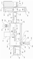
도 1은 일 실시 형태에 따른 기판 처리 시스템의 횡단면 개략도이다.
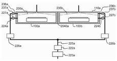
도 2는 일 실시 형태에 따른 기판 처리 시스템의 종단면 개략도이다.
도 3은 일 실시 형태에 따른 기판 처리 시스템의 진공 반송 로봇의 개략도이다.
도 4는 일 실시 형태에 따른 기판 처리 장치의 개략 구성도이다.
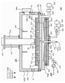
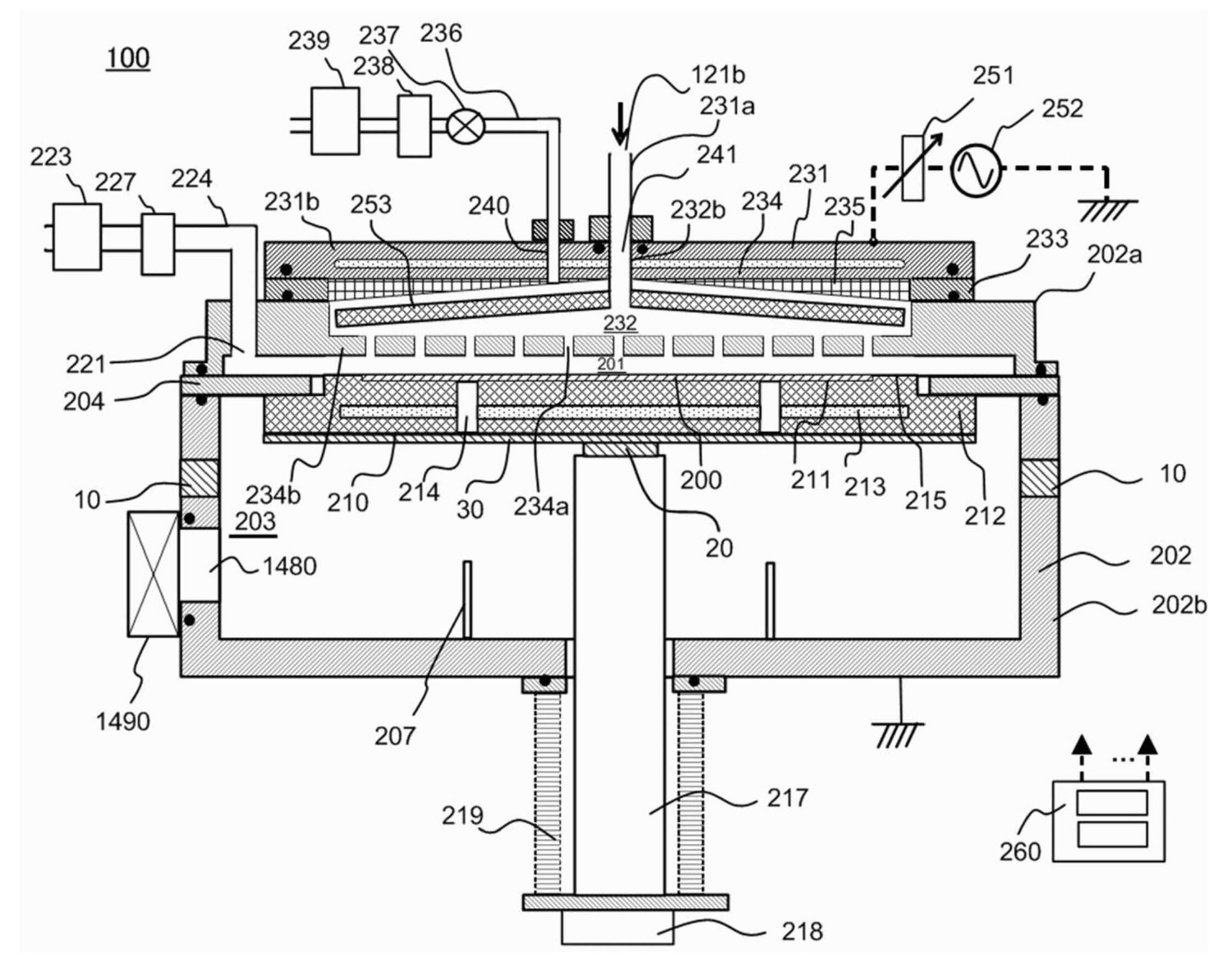
도 5는 일 실시 형태에 따른 챔버의 종단면 개략도이다.
도 6은 일 실시 형태에 따른 가스 공급계를 설명하기 위한 도면이다.
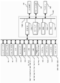
도 7은 일 실시 형태에 따른 기판 처리 시스템의 컨트롤러 개략 구성도이다.
도 8은 일 실시 형태에 따른 기판 처리 공정의 흐름도이다.
도 9는 일 실시 형태에 따른 기판 처리 공정의 시퀀스도이다.
도 10은 다른 실시 형태에 따른 챔버의 종단면 개략도이다.
도 11은 스트레스 완화 재의 변형예를 나타낸다.1 is a cross-sectional schematic view of a substrate processing system according to one embodiment.
2 is a schematic top view of a substrate processing system according to one embodiment.
3 is a schematic view of a vacuum carrying robot of the substrate processing system according to one embodiment.
4 is a schematic configuration diagram of a substrate processing apparatus according to one embodiment.
5 is a schematic top view of a chamber in accordance with one embodiment.
6 is a view for explaining a gas supply system according to an embodiment.
7 is a schematic configuration diagram of a controller of a substrate processing system according to an embodiment.
8 is a flowchart of a substrate processing process according to one embodiment.
9 is a sequence diagram of a substrate processing process according to an embodiment.
10 is a schematic top view of a chamber according to another embodiment.
Fig. 11 shows a modified example of the stress relieving material.
<제1 실시 형태>≪ First Embodiment >
이하에 본 발명의 제1 실시 형태를 도면을 참조하여 설명한다. 고온 프로세스에서는 서셉터나 반응실측으로부터의 열이 반응실의 하측(반송 공간: 이송실)에 전해져서 승온되기 때문에, 통상은 냉각수를 흘려서 필요한 온도 이하가 되도록 하고 있다. 그러나, 장치의 구조상 냉각시키기 어려운 부분이 있고, 이송실이 가열되어, 이송실이 연장되어, 기판 적재대의 위치(XYZ 방향)가 어긋남으로써, 가스 공급부와 기판과의 위치가 어긋나기 때문에, 기판에의 처리 균일성이 저하되는 과제가 있다. 본 발명은 상기한 열에 의한 이송실의 연장을 억제시키는 것이 가능한 기술을 제공하는 것을 목적으로 한다.BEST MODE FOR CARRYING OUT THE INVENTION A first embodiment of the present invention will be described below with reference to the drawings. In the high-temperature process, the heat from the susceptor or the reaction chamber side is transferred to the lower side (transfer space: transfer chamber) of the reaction chamber to raise the temperature, so that the cooling water is usually flowed to the required temperature or lower. However, since there is a part that is difficult to be cooled by the structure of the apparatus, the transfer chamber is heated, the transfer chamber is extended, and the position of the substrate mounting table (XYZ direction) is shifted, There is a problem that the processing uniformity of the film is deteriorated. It is an object of the present invention to provide a technique capable of suppressing the extension of the transfer chamber by the above-mentioned heat.
이하에, 본 실시 형태에 따른 기판 처리 시스템을 설명한다.Hereinafter, a substrate processing system according to the present embodiment will be described.
(1) 기판 처리 시스템의 구성(1) Configuration of substrate processing system
본 발명의 일 실시 형태에 따른 기판 처리 시스템의 개요 구성을, 도 1 내지 도 5를 사용해서 설명한다. 도 1은 본 실시 형태에 따른 기판 처리 시스템의 구성예를 도시하는 횡단면도이다. 도 2는, 본 실시 형태에 따른 기판 처리 시스템의 구성예를 도시하는 도 1의 α-α'에서의 종단면도이다. 도 3은 도 1의 아암의 상세를 설명한 설명도이다. 도 4는 도 1의 β-β'의 종단면도이며, 프로세스 모듈에 공급하는 가스 공급계를 설명하는 설명도이다. 도 5는, 프로세스 모듈에 설치되는 챔버를 설명하는 설명도이다.A schematic configuration of a substrate processing system according to an embodiment of the present invention will be described with reference to Figs. 1 to 5. Fig. 1 is a cross-sectional view showing a configuration example of a substrate processing system according to the present embodiment. Fig. 2 is a longitudinal sectional view at? -? 'Of Fig. 1 showing a structural example of a substrate processing system according to the present embodiment. Fig. 3 is an explanatory diagram for explaining the details of the arm of Fig. 1; Fig. 4 is a longitudinal sectional view of? -? 'In Fig. 1 and is an explanatory view for explaining a gas supply system for supplying the process module; Fig. 5 is an explanatory view for explaining a chamber installed in the process module. Fig.
도 1 및 도 2에서, 본 발명이 적용되는 기판 처리 시스템(1000)은, 웨이퍼(200)를 처리하는 것으로, IO 스테이지(1100), 대기 반송실(1200), 로드 로크실(1300), 진공 반송실(1400), 프로세스 모듈(110)로 주로 구성된다. 다음으로 각 구성에 대해서 구체적으로 설명한다. 도 1의 설명에서는, 전후 좌우는, X1 방향이 우, X2 방향이 좌, Y1 방향이 전, Y2 방향이 후로 한다.1 and 2, a
(대기 반송실·IO 스테이지)(Waiting transfer room, IO stage)
기판 처리 시스템(1000)의 앞쪽에는, IO 스테이지(로드 포트)(1100)가 설치되어 있다. IO 스테이지(1100) 상에는 복수의 포드(1001)가 탑재되어 있다. 포드(1001)는, 실리콘(Si) 기판 등의 기판(200)을 반송하는 캐리어로서 사용되고, 포드(1001) 내에는, 미처리의 기판(웨이퍼)(200)이나 처리가 끝난 기판(200)이 각각 수평 자세로 복수 저장되도록 구성되어 있다.In front of the
포드(1001)에는 캡(1120)이 설치되고, 후술하는 포드 오프너(1210)에 의해 개폐된다. 포드 오프너(1210)는, IO 스테이지(1100)에 적재된 포드(1001)의 캡(1120)을 개폐하여, 기판 출납구를 개방·폐쇄함으로써, 포드(1001)에 대한 기판(200)의 출납을 가능하게 한다. 포드(1001)는, 도시하지 않은 공정 내 반송 장치(RGV)에 의해, IO 스테이지(1100)에 대하여 공급 및 배출된다.The
IO 스테이지(1100)는, 대기 반송실(1200)에 인접한다. 대기 반송실(1200)은, IO 스테이지(1100)와 상이한 면에, 후술하는 로드 로크실(1300)이 연결된다.The IO
대기 반송실(1200) 내에는 기판(200)을 이동 탑재하는 제1 반송 로봇으로서의 대기 반송 로봇(1220)이 설치되어 있다. 도 2에 도시되어 있는 바와 같이, 대기 반송 로봇(1220)은, 대기 반송실(1200)에 설치된 엘리베이터(1230)에 의해 승강되도록 구성되어 있음과 함께, 리니어 액추에이터(1240)에 의해 좌우 방향으로 왕복 이동되도록 구성되어 있다.In the
도 2에 도시되어 있는 바와 같이, 대기 반송실(1200)의 상부에는 클린 에어를 공급하는 클린 유닛(1250)이 설치되어 있다. 또한, 도 1에 도시되어 있는 바와 같이, 대기 반송실(1200)의 좌측에는 기판(200)에 형성되어 있는 노치 또는 오리엔테이션 플랫을 맞추는 장치(이하, 프리얼라이너라고 함)(1260)가 설치되어 있다.As shown in Fig. 2, a
도 1 및 도 2에 도시되어 있는 바와 같이, 대기 반송실(1200)의 하우징(1270)의 전방측에는, 기판(200)을 대기 반송실(1200)에 대하여 반입 반출하기 위한 기판 반입 반출구(1280)와, 포드 오프너(1210)가 설치되어 있다. 기판 반입 반출구(1280)를 사이에 두고 포드 오프너(1210)와 반대측, 즉 하우징(1270)의 외측에는 IO 스테이지(로드 포트)(1100)가 설치되어 있다.1 and 2, a substrate loading /
대기 반송실(1200)의 하우징(1270)의 후방측에는, 웨이퍼(200)를 로드 로크실(1300)에 반입 반출하기 위한 기판 반입출구(1290)가 형성된다. 기판 반입출구(1290)는, 후술하는 게이트 밸브(1330)에 의해 개방·폐쇄됨으로써, 웨이퍼(200)의 출납을 가능하게 한다.A substrate loading and unloading
(로드 로크(L/L)실)(Load lock (L / L) thread)
로드 로크실(1300)은 대기 반송실(1200)에 인접한다. 로드 로크실(1300)을 구성하는 하우징(1310)이 갖는 면 중, 대기 반송실(1200)과는 상이한 면에는, 후술하는 바와 같이, 진공 반송실(1400)이 배치된다. 로드 로크실(1300)은, 대기 반송실(1200)의 압력과 진공 반송실(1400)의 압력에 맞춰서 하우징(1310) 내의 압력이 변동되기 때문에, 부압에 견딜 수 있는 구조로 구성되어 있다.The
하우징(1310) 중, 진공 반송실(1400)과 인접하는 측에는, 기판 반입 반출구(1340)가 형성된다. 기판 반입출구(1340)은, 게이트 밸브(1350)에 의해 개방·폐쇄됨으로써, 웨이퍼(200)의 출납을 가능하도록 한다.On the side of the
또한, 로드 로크실(1300) 내에는, 웨이퍼(200)를 적재하는 적재면(1311(1311a, 1311b))을 적어도 2개 갖는 기판 적재대(1320)가 설치되어 있다. 기판 적재면(1311) 사이의 거리는, 후술하는 진공 반송 로봇(1700)이 갖는 핑거간의 거리에 따라 설정된다.A substrate mounting table 1320 having at least two mounting surfaces 1311 (1311a, 1311b) for mounting the
(진공 반송실)(Vacuum transport chamber)
기판 처리 시스템(1000)은, 부압 하에서 기판(200)이 반송되는 반송 공간이 되는 반송실로서의 진공 반송실(트랜스퍼 모듈)(1400)을 구비하고 있다. 진공 반송실(1400)을 구성하는 하우징(1410)은, 평면에서 볼 때 오각형으로 형성되고, 오각형의 각 변에는, 로드 로크실(1300) 및 웨이퍼(200)를 처리하는 프로세스 모듈(110a 내지 110d)이 연결되어 있다. 진공 반송실(1400)의 대략 중앙부에는, 부압 하에서 기판(200)을 이동 탑재(반송)하는 제2 반송 로봇으로서의 진공 반송 로봇(1700)이 플랜지(1430)를 기초부로 해서 설치되어 있다. 또한, 여기에서는, 진공 반송실(1400)을 오각형인 예를 나타내지만, 사각형이나 육각형 등의 다각형이어도 된다.The
하우징(1410)의 측벽 중, 로드 로크실(1300)과 인접하는 측에는, 기판 반입 반출구(1420)가 형성되어 있다. 기판 반입출구(1420)는, 게이트 밸브(1350)에 의해 개방·폐쇄됨으로써, 웨이퍼(200)의 출납을 가능하게 한다.On the side of the
진공 반송실(1400) 내에 설치되는 진공 반송 로봇(1700)은, 도 2에 도시한 바와 같이, 엘리베이터(1450) 및 플랜지(1430)에 의해 진공 반송실(1400)의 기밀성을 유지하면서 승강할 수 있도록 구성되어 있다. 진공 반송 로봇(1700)의 상세한 구성은 후술한다. 엘리베이터(1450)는, 진공 반송 로봇(1700)이 갖는 2개의 아암(1800과 1900)을 각각 독립해서 승강 가능하도록 구성되어 있다.The
하우징(1410)의 천장이며, 하우징(1410) 내에 불활성 가스를 공급하기 위한 불활성 가스 공급 구멍(1460)이 형성된다. 불활성 가스 공급 구멍(1460)에는 불활성 가스 공급관(1510)이 설치된다. 불활성 가스 공급관(1510)에는 상류에서부터 순서대로 불활성 가스원(1520), 매스 플로우 컨트롤러(1530), 밸브(1540)가 설치되어, 하우징(1410) 내에 공급하는 불활성 가스의 공급량을 제어하고 있다.An inert
주로, 불활성 가스 공급관(1510), 매스 플로우 컨트롤러(1530), 밸브(1540)로, 진공 반송실(1400)에 있어서의 불활성 가스 공급부(1500)가 구성된다. 또한, 불활성 가스원(1520), 불활성 가스 공급 구멍(1460)을 불활성 가스 공급부(1500)에 포함해도 된다.An inert
하우징(1410)의 저벽에는, 하우징(1410)의 분위기를 배기하기 위한 배기 구멍(1470)이 형성된다. 배기 구멍(1470)에는, 배기관(1610)이 설치된다. 배기관(1610)에는, 상류에서부터 순서대로 압력 제어기인 APC(Auto Pressure Controller)(1620), 펌프(1630)가 설치된다.An
주로, 배기관(1610), APC(1620)로 진공 반송실(1400)에 있어서의 가스 배기부(1600)가 구성된다. 또한, 펌프(1630), 배기 구멍(1470)을 가스 배기부에 포함해도 된다.The
불활성 가스 공급부(1500), 가스 배기부(1600)의 협동에 의해 진공 반송실(1400)의 분위기가 제어된다. 예를 들어, 하우징(1410) 내의 압력이 제어된다.The atmosphere of the
도 1에 도시되어 있는 바와 같이, 하우징(1410)에 5매의 측벽 중, 로드 로크실(1300)이 설치되어 있지 않은 측에는, 웨이퍼(200)에 원하는 처리를 행하는 프로세스 모듈(110a, 110b, 110c, 110d)이 연결되어 있다.1, a
프로세스 모듈(110a, 110b, 110c, 110d)의 각각에는, 기판 처리 장치의 일 구성인 챔버(100)가 설치되어 있다. 구체적으로는, 프로세스 모듈(110a)은, 챔버(100a, 100b)가 설치된다. 프로세스 모듈(110b)에는 챔버(100c, 100d)가 설치된다. 프로세스 모듈(110c)에는 챔버(100e, 100f)가 설치된다. 프로세스 모듈(110d)에는 챔버(100g, 100h)가 설치된다.Each of the
하우징(1410)의 측벽 중, 각 챔버(100)와 대향하는 벽에는 기판 반입출구(1480)이 형성된다. 예를 들어, 도 2에 기재한 바와 같이, 챔버(100e)와 대향하는 벽에는, 기판 입출구(1480e)가 형성된다.A substrate loading /
도 2 중, 챔버(100e)를 챔버(100a)로 치환한 경우, 챔버(100a)와 대향하는 벽에는, 기판 반입 반출구(1480a)가 형성된다.2, when the
마찬가지로, 챔버(100f)를 챔버(100b)로 치환한 경우, 챔버(100b)와 대향하는 벽에는, 기판 반입 반출구(1480b)가 형성된다.Likewise, when the
게이트 밸브(1490)는, 도 1에 도시되어 있는 바와 같이, 처리실마다 설치된다. 구체적으로는, 챔버(100a)와 진공 반송실(1400)과의 사이에는 게이트 밸브(1490a)가, 챔버(100b)와의 사이에는 게이트 밸브(1490b)가 설치된다. 챔버(100c)와의 사이에는 게이트 밸브(1490c)가, 챔버(100d)와의 사이에는 게이트 밸브(1490d)가 설치된다. 챔버(100e)와의 사이에는 게이트 밸브(1490e)가, 챔버(100f)와의 사이에는 게이트 밸브(1490f)가 설치된다. 챔버(100g)와의 사이에는 게이트 밸브(1490g)가, 챔버(100h)와의 사이에는 게이트 밸브(1490h)가 설치된다.The
각 게이트 밸브(1490)에 의해 개방·폐쇄됨으로써, 기판 반입출구(1480)를 통한 웨이퍼(200)의 출납을 가능하게 한다.And is opened / closed by each
계속해서, 진공 반송실(1400)에 탑재되는 진공 반송 로봇(1700)에 대해서, 도 3을 사용해서 설명한다. 도 3은 도 1의 진공 반송 로봇(1700)을 확대한 도면이다.Next, the
진공 반송 로봇(1700)은, 2개의 아암(1800)과 아암(1900)을 구비한다. 아암(1800)은, 선단에 2개의 엔드 이펙터(1810)와 엔드 이펙터(1820)가 설치된 포크 포션(1830)을 갖는다. 포크 포션(1830)의 근원에는 미들 포션(1840)이 축(1850)을 통해서 접속된다.The
엔드 이펙터(1810)와 엔드 이펙터(1820)에는, 각각의 프로세스 모듈(110)로부터 반출되는 웨이퍼(200)가 적재된다. 도 2에서는, 프로세스 모듈(110c)로부터 반출되는 웨이퍼(200)가 적재되는 예를 나타낸다.The
미들 포션(1840) 중, 포크 포션(1830)과 상이한 개소에는, 보텀 포션(1860)이 축(1870)을 통해서 접속된다. 보텀 포션(1860)은, 축(1880)을 통해서 플랜지(1430)에 배치된다.A
아암(1900)은, 선단에 2개의 엔드 이펙터(1910)와 엔드 이펙터(1920)가 설치된 포크 포션(1930)을 갖는다. 포크 포션(1930)의 근원에는 미들 포션(1940)이 축(1950)을 통해서 접속된다.The
엔드 이펙터(1910)와 엔드 이펙터(1920)에는, 로드 로크실(1300)로부터 반출되는 웨이퍼(200)가 적재된다.The
미들 포션(1940) 중, 포크 포션(1930)과 상이한 개소에는, 보텀 포션(1960)이 축(1970)을 통해서 접속된다. 보텀 포션(1960)은, 축(1980)을 통해서 플랜지(1430)에 배치된다.A
엔드 이펙터(1810), 엔드 이펙터(1820)는, 엔드 이펙터(1910), 엔드 이펙터(1920)보다도 높은 위치에 배치된다.The
진공 반송 로봇(1700)은 축을 중심으로 한 회전이나, 아암의 연신이 가능하다.The
(프로세스 모듈)(Process module)
계속해서 각 프로세스 모듈(110) 중, 프로세스 모듈(110a)에 대해서, 도 1, 도 2, 도 4를 예로 들어 설명한다. 도 4는 프로세스 모듈(110a)과 프로세스 모듈(110a)에 접속되는 가스 공급부와, 프로세스 모듈(110a)에 접속되는 가스 배기부와의 관련을 설명하는 설명도이다.Next, the
여기에서는 프로세스 모듈(110a)을 예로 들고 있지만, 다른 프로세스 모듈(110b), 프로세스 모듈(110c), 프로세스 모듈(110d)에서도 마찬가지의 구조이기 때문에, 여기에서는 설명을 생략한다.Although the
도 4에 기재한 바와 같이, 프로세스 모듈(110a)에는, 웨이퍼(200)를 처리하는 기판 처리 장치의 일 구성의 챔버(100a)와 챔버(100b)가 설치된다. 챔버(100a)와 챔버(100b)의 사이에는 격벽(2040a)이 설치되고, 각각의 챔버 내의 분위기가 혼재되지 않도록 구성된다.As shown in Fig. 4, the
도 2에 기재한 바와 같이, 챔버(100e)와 진공 반송실(1400)이 인접하는 벽에는, 기판 반입 반출구(2060e)가 형성되고, 마찬가지로, 챔버(100a)와 진공 반송실(1400)이 인접하는 벽에는 기판 반입출구(2060a)가 형성되어 있다.2, a substrate carry-in / out
각 챔버(100)에는 웨이퍼(200)를 지지하는 기판 지지부(210)가 설치되어 있다.Each
프로세스 모듈(110a)에는, 챔버(100a)와 챔버(100b)의 각각에 처리 가스를 공급하는 가스 공급부가 접속되어 있다. 가스 공급부는, 제1 가스 공급부(처리 가스 공급부), 제2 가스 공급부(반응 가스 공급부), 제3 가스 공급부(제1 퍼지 가스 공급부), 제4 가스 공급부(제2 퍼지 가스 공급부) 등으로 구성된다. 각 가스 공급부의 구성에 대해서 설명한다.The
(1) 기판 처리 장치의 구성(1) Configuration of substrate processing apparatus
제1 실시 형태에 따른 기판 처리 장치에 대해서 설명한다.The substrate processing apparatus according to the first embodiment will be described.
본 실시 형태에 따른 기판 처리 장치(100)에 대해서 설명한다. 기판 처리 장치(100)는, 고유전율 절연막 형성 유닛이며, 도 1에 도시되어 있는 바와 같이, 낱장식 기판 처리 장치로서 구성되어 있다. 기판 처리 장치에서는, 상술한 바와 같은 반도체 디바이스의 제조의 일 공정이 행하여진다.The
도 5에 도시하는 바와 같이, 기판 처리 장치(100)는, 처리 용기(202)를 구비하고 있다. 처리 용기(202)는, 예를 들어 횡단면이 원형이며 편평한 밀폐 용기로 구성되어 있다. 또한, 처리 용기(202)는, 예를 들어 알루미늄(Al)이나 스테인리스(SUS) 등의 금속 재료, 또는, 석영에 의해 구성되어 있다. 처리 용기(202) 내에는, 기판으로서의 실리콘 웨이퍼 등의 웨이퍼(200)를 처리하는 처리 공간(처리실)(201), 반송 공간(이송실)(203)이 형성되어 있다. 처리 용기(202)는, 상부 용기(202a)와 하부 용기(202b)로 구성된다. 상부 용기(202a)와 하부 용기(202b)의 사이에는 구획판(204)이 설치된다. 상부 처리 용기(202a)에 둘러싸인 공간이며, 구획판(204)보다도 상방의 공간을 처리 공간(처리실이라고도 말함)(201)이라 칭하고, 하부 용기(202b)에 둘러싸인 공간이며, 구획판(204)보다도 하방의 공간을 반송 공간(203)이라 칭한다.As shown in Fig. 5, the
하부 용기(202b)의 측면에는, 게이트 밸브(1490)에 인접한 기판 반입출구(1480)가 형성되어 있고, 웨이퍼(200)는, 기판 반입출구(1480)를 통해서 도시하지 않은 반송실과의 사이를 이동한다. 하부 용기(202b)의 저부에는, 리프트 핀(207)이 복수 설치되어 있다. 또한, 하부 용기(202b)는 접지되어 있다.A substrate carry-in / out
여기서, 상부 용기(202a)의 구성 재료인 석영의 팽창 계수는, 6×10^-7/℃이고, 저온 시와 고온 시의 온도 차ΔT=300℃일 때, 약 0.05mm 내지 0.4mm 정도 신장되는 경우가 있다. 하부 용기(202b)의 구성 재료가 알루미늄인 경우에는, 알루미늄의 팽창 계수가 23×10^-6/℃이고 저온 시와 고온 시의 온도 차ΔT=300℃ 정도로, 약 2.0mm 내지 14mm 정도 신장되는 경우가 있다. 또한, 신장 길이(ΔL)는, ΔL=L×α×ΔT로 산출된다. 여기서, L은 재료의 길이[mm], α는 열팽창 계수[/℃], ΔT[℃]는 온도 차이다.The expansion coefficient of quartz as a constituent material of the
이와 같이, 신장 길이(변화량)는 재료에 따라 상이하다. 변화량의 차에 따라, 기판 적재대(212)와 샤워 헤드(234)와의 중심 위치 관계(XY 방향의 위치 관계)가 어긋나서, 처리 균일성이 저하되어버리는 과제가 있다. 또한, Z 방향이 신장되는 길이(변화량)의 차에 의해, 적재면(211)과 분산판(234b)과의 거리가 변화하여, 처리실(201) 내의 배기 컨덕턴스나, 처리실(201)로부터 배기구(221)까지의 배기 컨덕턴스가 변화해서 처리 균일성이 저하되는 과제가 있다. 또한, 반송실(1400)의 중심 위치와 프로세스 모듈(110a)의 중심 위치와의 사이의 거리가 신장되어, 웨이퍼(200)를 적재면(211)의 중심으로 반송할 수 없게 되는 과제가 있다. 또한, 챔버(100a)의 중심 위치와 챔버(100b)의 중심 위치의 사이의 거리가 신장되어, 웨이퍼(200)를 적재면(211)의 중심으로 반송할 수 없게 되는 과제가 있다.As such, the elongation length (variation) varies depending on the material. The center positional relationship (positional relationship in the X and Y directions) between the substrate mounting table 212 and the
따라서, 본 실시 형태에서는, 하부 용기(202b)의 측면의, 게이트 밸브(1490)보다 상측의 위치에, 제1 단열부(10)가 설치되어 있다. 제1 단열부(10)는, 후술하는 제2 단열부보다 Z 방향(높이 방향)에 있어서, 하측에 설치되어 있다. 제1 단열부(10)를 설치함으로써, 하측 용기(202b)의 XY 방향·Z 방향으로의 신장을 억제하여, 이들 과제를 해결하는 것이 가능하게 된다. 또한, 여기에서는, 프로세스 모듈(110a)에 대해서 기재했지만, 다른 프로세스 모듈(110b, 110c, 110d)도 마찬가지이다.Therefore, in the present embodiment, the first
제1 단열부(10)는, 예를 들어 내열 수지, 유전 수지, 석영, 그래파이트 등 중 어느 하나, 또는, 복합된 열전도율이 낮은 재료로 구성되며, 링 형상으로 구성된다.The first
처리실(201) 내에는, 웨이퍼(200)를 지지하는 기판 지지부(210)가 설치되어 있다. 기판 지지부(210)는, 웨이퍼(200)를 적재하는 적재면(211)과, 적재면(211)과 외주면(215)을 표면에 갖는 기판 적재대(212)를 갖는다. 바람직하게는, 가열부로서의 히터(213)를 설치한다. 가열부를 설치함으로써, 기판을 가열시켜, 기판 상에 형성되는 막의 품질을 향상시킬 수 있다. 기판 적재대(212)에는, 리프트 핀(207)이 관통하는 관통 구멍(214)이 리프트 핀(207)과 대응하는 위치에 각각 형성되어 있어도 된다. 또한, 기판 적재대(212)의 표면에 형성된 적재면(211)의 높이를 외주면(215)보다도 웨이퍼(200)의 두께에 상당하는 길이만큼 낮게 형성해도 된다. 이와 같이 구성함으로써, 웨이퍼(200)의 상면의 높이와 기판 적재대(212)의 외주면(215)과의 높이의 차가 작아져, 차에 의해 발생하는 가스의 난류를 억제할 수 있다. 또한, 가스의 난류가 웨이퍼(200)에의 처리 균일성에 영향을 주지 않는 경우에는, 외주면(215)의 높이를 적재면(211)과 동일 평면 상의 높이 이상이 되도록 구성해도 된다.In the
기판 적재대(212)는 샤프트(217)에 의해 지지된다. 샤프트(217)는, 처리 용기(202)의 저부를 관통하고 있고, 또한 처리 용기(202)의 외부에서 승강 기구(218)에 접속되어 있다. 승강 기구(218)를 작동시켜서 샤프트(217) 및 기판 적재대(212)를 승강시킴으로써, 기판 적재면(211) 상에 적재되는 웨이퍼(200)를 승강시키는 것이 가능하게 구성된다. 또한, 샤프트(217) 하단부의 주위는 벨로즈(219)에 의해 덮여 있어, 처리실(201) 내는 기밀하게 유지되어 있다. 샤프트(217)와 기판 적재대(212)의 사이에는 제2 단열부(20)가 설치되어 있다. 이 제2 단열부(20)는, 상기한 히터(213)로부터의 열이 샤프트(217)나, 반송 공간(203)에 전해지는 것을 억제하는 역할을 하고 있다. 제2 단열부(20)는, 바람직하게는 게이트 밸브(1490)보다도 상측에 설치되어 있다. 보다 바람직하게는, 제2 단열부(20)의 직경을 샤프트(217)의 직경보다도 짧게 구성한다. 이에 의해, 히터(213)로부터 샤프트(217)에의 열전도를 억제할 수 있어, 기판 적재대(212)의 온도 균일성을 향상시킬 수 있다. 또한, 기판 적재부(212)의 하측이며, 제2 단열부(20)과의 사이, 환언하면, 히터(213)보다도 하측이며, 제2 단열부(20)보다도 상측에는, 히터(213)로부터의 열을 반사하는 반사부(30)가 설치되어 있다.The substrate mount table 212 is supported by a
반사부(30)를 제2 단열부(20)보다도 상측에 설치함으로써, 히터(213)로부터의 방사열을 하부 용기(202b)의 내벽에 방사시키지 않고, 반사시킬 수 있다. 또한, 반사 효율을 향상시킬 수 있어, 히터(213)의 기판(200)에의 가열 효율을 향상시킬 수 있다. 반사부(30)를 제2 단열부(20)의 하측에 설치한 경우에는, 히터(213)로부터의 열은, 제2 단열부(20)에서 흡수되어 버리기 때문에, 히터(213)에의 반사량이 저하되어, 히터(213)의 가열 효율이 저하된다. 또한, 제2 단열부(20)가 가열되어, 제2 단열부(20)에 의해 샤프트(217)가 가열되어버리는 것을 억제하는 것이 가능하게 된다.The
기판 적재대(212)는, 웨이퍼(200)의 반송 시에는, 기판 적재면(211)이 기판 반입출구(206)의 위치(웨이퍼 반송 위치)가 되도록 하강하고, 웨이퍼(200)의 처리 시에는 도 1에서 나타낸 바와 같이, 웨이퍼(200)가 처리실(201) 내의 처리 위치(웨이퍼 처리 위치)까지 상승한다.The substrate mounting table 212 is lowered so that the
구체적으로는, 기판 적재대(212)를 웨이퍼 반송 위치까지 하강시켰을 때는, 리프트 핀(207)의 상단부가 기판 적재면(211)의 상면으로부터 돌출되어, 리프트 핀(207)이 웨이퍼(200)를 하방으로부터 지지하도록 되어 있다. 또한, 기판 적재대(212)를 웨이퍼 처리 위치까지 상승시켰을 때는, 리프트 핀(207)은 기판 적재면(211)의 상면으로부터 매몰되어, 기판 적재면(211)이 웨이퍼(200)를 하방으로부터 지지하도록 되어 있다. 또한, 리프트 핀(207)은, 웨이퍼(200)와 직접 접촉하기 때문에, 예를 들어 석영이나 알루미나 등의 재질로 형성하는 것이 바람직하다. 또한, 리프트 핀(207)에 승강 기구를 설치하고, 기판 적재대(212)와 리프트 핀(207)이 상대적으로 움직이도록 구성해도 된다. 이 처리 위치에서, 제1 단열부(10)는 게이트 밸브(1490)보다도 상측에 설치되고, 제2 단열부(20)의 높이보다도 하측에 설치되어 있다.More specifically, when the substrate stacking table 212 is lowered to the wafer transfer position, the upper end of the
제2 단열부(20)를 제1 단열부(10)보다도 상측에 설치함으로써, 샤프트(217)로부터 하부 용기(202b)의 내벽에의 방열량을 억제시킬 수 있다는 효과가 있다. 또한, 샤프트(217)로부터 방열되었다고 해도, 샤프트(217)와 대향하는 하부 용기(202b)의 내벽이 받은 열이 게이트 밸브(1490)측에 열전도되는 것을 억제할 수 있다는 효과가 있다.The second
또한, 제1 단열부(10)를 후술하는 배기구(221)의 근방에 설치하는 구성으로 해도 된다. 이 구성에 의하면, 배기구(221)에는 고온의 가스가 흘러 오기 때문에, 배기구(221)의 근처에서 단열하지 않으면, 처리 용기(202)를 구성하는 벽이나 이송실 공간(203) 등을 통하여, 다양한 부위가 가열되어버리는 것을 억제시키는 것이 가능하게 된다.Further, the first
(배기계)(Exhaust system)
처리실(201)(상부 용기(202a))의 내벽 상면에는, 처리실(201)의 분위기를 배기하는 제1 배기부로서의 배기구(221)가 형성되어 있다. 배기구(221)에는 제1 배기관으로서의 배기관(224)이 접속되어 있고, 배기관(224)에는, 처리실(201) 내를 소정의 압력으로 제어하는 APC(Auto Pressure Controller) 등의 압력 조정기(222a), 진공 펌프(223)가 순서대로 직렬로 접속되어 있다. 주로, 배기구(221), 배기관(224), 압력 조정기(227)에 의해, 제1 배기부(배기 라인)가 구성된다. 또한, 진공 펌프(223)를 제1 배기부에 포함하도록 구성해도 된다.On the upper surface of the inner wall of the process chamber 201 (
버퍼 공간(232)의 내벽 상면의 샤워 헤드(234)의 상부에는, 버퍼 공간(232)의 분위기를 배기하는 제2 배기부로서의 샤워 헤드 배기구(240)가 형성되어 있다. 샤워 헤드 배기구(240)에는 제2 배기관으로서의 배기관(236)이 접속되어 있고, 배기관(236)에는, 밸브(237), 버퍼 공간(232) 내를 소정의 압력으로 제어하는 APC(Auto Pressure Controller) 등의 압력 조정기(238), 진공 펌프(239)가 순서대로 직렬로 접속되어 있다. 주로, 샤워 헤드 배기구(240), 밸브(237), 배기관(236), 압력 조정기(238)에 의해, 제2 배기부(배기 라인)가 구성된다. 또한, 진공 펌프(239)를 제2 배기부에 포함하도록 구성해도 된다. 또한, 진공 펌프(239)를 설치하지 않고, 배기관(236)을 진공 펌프(223)에 접속하도록 구성해도 된다.A
(가스 도입구)(Gas inlet)
처리실(201)의 상부에 설치되는 샤워 헤드(234)의 상면(천장벽)에는, 처리실(201) 내에 각종 가스를 공급하기 위한 가스 도입구(241)가 형성되어 있다. 가스 공급부인 제1 가스 도입구(241)에 접속되는 가스 공급 유닛의 구성에 대해서는 후술한다.A
(가스 분산부)(Gas dispersion part)
샤워 헤드(234)는, 버퍼 실(공간)(232), 분산판(234b), 분산 구멍(234a)에 의해 구성되어 있다. 샤워 헤드(234)는, 가스 도입구(241)와 처리실(201)과의 사이에 설치되어 있다. 가스 도입구(241)로부터 도입되는 가스는 샤워 헤드(234)의 버퍼 공간(232)(분산부)에 공급된다. 샤워 헤드(234)는, 예를 들어 석영, 알루미나, 스테인리스, 알루미늄 등의 재료로 구성된다.The
또한, 샤워 헤드(234)의 덮개(231)를 도전성이 있는 금속으로 형성하고, 버퍼 공간(232) 또는 처리실(201) 내에 존재하는 가스를 여기하기 위한 활성화부(여기부)로 해도 된다. 이때는, 덮개(231)와 상부 용기(202a)와의 사이에는 절연 블록(233)이 설치되어, 덮개(231)와 상부 용기(202a)의 사이를 절연하고 있다. 활성화부로서의 전극(덮개(231))에는, 정합기(251)와 고주파 전원(252)을 접속하여, 전자파(고주파 전력이나 마이크로파)가 공급 가능하게 구성되어도 된다.The
버퍼 공간(232)에는, 가스 도입구(241)로부터 도입된 가스를 버퍼 공간(232)에 확산시키기 위한 분산판(253)이 설치되어 있다.The
(처리 가스 공급부)(Process gas supply unit)
분산판(253)에 접속된 가스 도입구(241)에는, 공통 가스 공급관(242)이 접속되어 있다. 도 6에 나타낸 바와 같이, 공통 가스 공급관(242)에는, 제1 가스 공급관(243a), 제2 가스 공급관(244a), 제3 가스 공급관(245a), 클리닝 가스 공급관(248a)이 접속되어 있다.A common
제1 가스 공급관(243a)을 포함하는 제1 가스 공급부(243)로부터는 제1 원소 함유 가스(제1 처리 가스)가 주로 공급되고, 제2 가스 공급관(244a)을 포함하는 제2 가스 공급부(244)로부터는 주로 제2 원소 함유 가스(제2 처리 가스)가 공급된다. 제3 가스 공급관(245a)을 포함하는 제3 가스 공급부(245)로부터는, 주로 퍼지 가스가 공급되고, 클리닝 가스 공급관(248a)을 포함하는 클리닝 가스 공급부(248)로부터는 클리닝 가스가 공급된다. 처리 가스를 공급하는 처리 가스 공급부는, 제1 처리 가스 공급부와 제2 처리 가스 공급부 중 어느 하나 또는 양쪽으로 구성되고, 처리 가스는, 제1 처리 가스와 제2 처리 가스 중 어느 하나 또는 양쪽으로 구성된다.Containing gas (first process gas) is mainly supplied from the first
(제1 가스 공급부)(First gas supply unit)
제1 가스 공급관(243a)에는, 상류 방향에서부터 순서대로, 제1 가스 공급원(243b), 유량 제어기(유량 제어부)인 매스 플로우 컨트롤러(MFC)(243c) 및 개폐 밸브인 밸브(243d)가 설치되어 있다.The first
제1 가스 공급원(243b)으로부터, 제1 원소를 함유하는 가스(제1 처리 가스)가 공급되고, 매스 플로우 컨트롤러(243c), 밸브(243d), 제1 가스 공급관(243a), 공통 가스 공급관(242)을 통해서 버퍼 공간(232)에 공급된다.The gas containing the first element (the first processing gas) is supplied from the first
제1 처리 가스는, 원료 가스, 즉, 처리 가스의 하나이다.The first process gas is one of a source gas, that is, a process gas.
여기서, 제1 원소는, 예를 들어 실리콘(Si)이다. 즉, 제1 처리 가스는, 예를 들어 실리콘 함유 가스이다. 실리콘 함유 가스로서는, 예를 들어 디클로로실란(Dichlorosilane(SiH2Cl2): DCS) 가스를 사용할 수 있다. 또한, 제1 처리 가스의 원료는, 상온 상압에서 고체, 액체 및 기체 중 어느 것이어도 된다. 제1 처리 가스의 원료가 상온 상압에서 액체인 경우에는, 제1 가스 공급원(243b)과 매스 플로우 컨트롤러(243c)와의 사이에, 도시하지 않은 기화기를 설치하면 된다. 여기에서는 원료는 기체로서 설명한다.Here, the first element is, for example, silicon (Si). That is, the first process gas is, for example, a silicon-containing gas. As the silicon-containing gas, for example, dichlorosilane (SiH 2 Cl 2 ): DCS) gas can be used. The raw material of the first process gas may be any of solid, liquid and gas at room temperature and normal pressure. When the raw material of the first process gas is liquid at room temperature and normal pressure, a vaporizer (not shown) may be provided between the first
제1 가스 공급관(243a)의 밸브(243d)보다도 하류측에는, 제1 불활성 가스 공급관(246a)의 하류단이 접속되어 있다. 제1 불활성 가스 공급관(246a)에는, 상류 방향에서부터 순서대로, 불활성 가스 공급원(246b), 유량 제어기(유량 제어부)인 매스 플로우 컨트롤러(MFC)(246c) 및 개폐 밸브인 밸브(246d)가 설치되어 있다.A downstream end of the first inert
여기서, 불활성 가스는, 예를 들어 질소(N2) 가스이다. 또한, 불활성 가스로서, N2 가스 이외에, 예를 들어 헬륨(He) 가스, 네온(Ne) 가스, 아르곤(Ar) 가스 등의 희가스를 사용할 수 있다.Here, the inert gas is, for example, nitrogen (N 2 ) gas. In addition to the N 2 gas, a rare gas such as helium (He) gas, Neon (Ne) gas or argon (Ar) gas may be used as the inert gas.
주로, 제1 가스 공급관(243a), 매스 플로우 컨트롤러(243c), 밸브(243d)에 의해, 제1 원소 함유 가스 공급부(243)(실리콘 함유 가스 공급부라고도 함)가 구성된다.The first element gas supply section 243 (also referred to as a silicon-containing gas supply section) is constituted mainly by the first
또한, 주로, 제1 불활성 가스 공급관(246a), 매스 플로우 컨트롤러(246c) 및 밸브(246d)에 의해 제1 불활성 가스 공급부가 구성된다. 또한, 불활성 가스 공급원(246b), 제1 가스 공급관(243a)을 제1 불활성 가스 공급부에 포함해서 생각해도 된다.Also, the first inert gas supply section is mainly constituted by the first inert
또한, 제1 가스 공급원(243b), 제1 불활성 가스 공급부를, 제1 원소 함유 가스 공급부에 포함해서 생각해도 된다.The first
(제2 가스 공급부)(Second gas supply part)
제2 가스 공급관(244a)의 상류에는, 상류 방향에서부터 순서대로, 제2 가스 공급원(244b), 유량 제어기(유량 제어부)인 매스 플로우 컨트롤러(MFC)(244c) 및 개폐 밸브인 밸브(244d)가 설치되어 있다.A second
제2 가스 공급원(244b)으로부터, 제2 원소를 함유하는 가스(이하, 「제2 처리 가스」)가 공급되고, 매스 플로우 컨트롤러(244c), 밸브(244d), 제2 가스 공급관(244a), 공통 가스 공급관(242)을 통해서 버퍼 공간(232)에 공급된다.A gas containing a second element is supplied from the second
제2 처리 가스는, 처리 가스의 하나이다. 또한, 제2 처리 가스는, 반응 가스 또는 개질 가스로서 생각해도 된다.The second process gas is one of the process gases. Further, the second process gas may be considered as a reactive gas or a reformed gas.
여기서, 제2 처리 가스는, 제1 원소와 상이한 제2 원소를 함유한다. 제2 원소로서는, 예를 들어 산소(O), 질소(N), 탄소(C), 수소(H) 중 1개 이상을 포함하고 있다. 본 실시 형태에서는, 제2 처리 가스는, 예를 들어 질소 함유 가스인 것으로 한다. 구체적으로는, 질소 함유 가스로서는, 암모니아(NH3) 가스가 사용된다.Here, the second process gas contains a second element different from the first element. The second element includes at least one of oxygen (O), nitrogen (N), carbon (C), and hydrogen (H), for example. In the present embodiment, the second process gas is, for example, a nitrogen-containing gas. Specifically, as the nitrogen-containing gas, ammonia (NH 3 ) gas is used.
주로, 제2 가스 공급관(244a), 매스 플로우 컨트롤러(244c), 밸브(244d)에 의해, 제2 처리 가스 공급부(244)가 구성된다.The second process
그 외에도, 활성화부로서의 리모트 플라즈마 유닛(RPU)(244e)을 설치하여, 제2 처리 가스를 활성화 가능하도록 구성해도 된다.In addition, a remote plasma unit (RPU) 244e as an activation unit may be provided to activate the second process gas.
또한, 제2 가스 공급관(244a)의 밸브(244d)보다도 하류측에는, 제2 불활성 가스 공급관(247a)의 하류단이 접속되어 있다. 제2 불활성 가스 공급관(247a)에는, 상류 방향에서부터 순서대로, 불활성 가스 공급원(247b), 유량 제어기(유량 제어부)인 매스 플로우 컨트롤러(MFC)(247c) 및 개폐 밸브인 밸브(247d)가 설치되어 있다.A downstream end of the second inert
불활성 가스 공급원(247b)으로부터는, 불활성 가스가, 매스 플로우 컨트롤러(247c), 밸브(247d), 제2 불활성 가스 공급관(247a)을 통해서 버퍼 공간(232)에 공급된다. 불활성 가스는, 박막 형성 공정(후술하는 S203 내지 S207)에서는 캐리어 가스 또는 희석 가스로서 작용한다.Inert gas is supplied from the inert
주로, 제2 불활성 가스 공급관(247a), 매스 플로우 컨트롤러(247c) 및 밸브(247d)에 의해 제2 불활성 가스 공급부가 구성된다. 또한, 불활성 가스 공급원(247b), 제2 가스 공급관(244a)을 제2 불활성 가스 공급부에 포함해서 생각해도 된다.The second inert gas supply portion is mainly constituted by the second inert
또한, 제2 가스 공급원(244b), 제2 불활성 가스 공급부를, 제2 원소 함유 가스 공급부(244)에 포함해서 생각해도 된다.The second
(제3 가스 공급부)(Third gas supply unit)
제3 가스 공급관(245a)에는, 상류 방향에서부터 순서대로, 제3 가스 공급원(245b), 유량 제어기(유량 제어부)인 매스 플로우 컨트롤러(MFC)(245c) 및 개폐 밸브인 밸브(245d)가 설치되어 있다.The third
제3 가스 공급원(245b)으로부터, 퍼지 가스로서의 불활성 가스가 공급되고, 매스 플로우 컨트롤러(245c), 밸브(245d), 제3 가스 공급관(245a), 공통 가스 공급관(242)을 통해서 버퍼 공간(232)에 공급된다.Inert gas as purge gas is supplied from the third
여기서, 불활성 가스는, 예를 들어 질소(N2) 가스이다. 또한, 불활성 가스로서, N2 가스 이외에, 예를 들어 헬륨(He) 가스, 네온(Ne) 가스, 아르곤(Ar) 가스 등의 희가스를 사용할 수 있다.Here, the inert gas is, for example, nitrogen (N 2 ) gas. In addition to the N 2 gas, a rare gas such as helium (He) gas, Neon (Ne) gas or argon (Ar) gas may be used as the inert gas.
주로, 제3 가스 공급관(245a), 매스 플로우 컨트롤러(245c), 밸브(245d)에 의해, 제3 가스 공급부(245)(퍼지 가스 공급부라고도 함)가 구성된다.A third gas supply section 245 (also referred to as a purge gas supply section) is constituted mainly by the third
(클리닝 가스 공급부)(Cleaning gas supply unit)
클리닝 가스 공급관(248a)에는, 상류 방향에서부터 순서대로, 클리닝 가스원(248b), 매스 플로우 컨트롤러(MFC)(248c), 밸브(248d), 리모트 플라즈마 유닛(RPU)(250)이 설치되어 있다.A cleaning
클리닝 가스원(248b)으로부터, 클리닝 가스가 공급되고, MFC(248c), 밸브(248d), RPU(250), 클리닝 가스 공급관(248a), 공통 가스 공급관(242)을 통해서 버퍼 공간(232)에 공급된다.A cleaning gas is supplied from the cleaning
클리닝 가스 공급관(248a)의 밸브(248d)보다도 하류측에는, 제4 불활성 가스 공급관(249a)의 하류단이 접속되어 있다. 제4 불활성 가스 공급관(249a)에는, 상류 방향에서부터 순서대로, 제4 불활성 가스 공급원(249b), MFC(249c), 밸브(249d)가 설치되어 있다.On the downstream side of the
또한, 주로, 클리닝 가스 공급관(248a), MFC(248c) 및 밸브(248d)에 의해 클리닝 가스 공급부가 구성된다. 또한, 클리닝 가스원(248b), 제4 불활성 가스 공급관(249a), RPU(250)를, 클리닝 가스 공급부에 포함해서 생각해도 된다.Also, the cleaning gas supply unit is mainly constituted by the cleaning
또한, 제4 불활성 가스 공급원(249b)으로부터 공급되는 불활성 가스를, 클리닝 가스의 캐리어 가스 또는 희석 가스로서 작용하도록 공급해도 된다.Alternatively, the inert gas supplied from the fourth inert
클리닝 가스 공급원(248b)으로부터 공급되는 클리닝 가스는, 클리닝 공정에서는 샤워 헤드(234)나 처리실(201)에 부착된 부생성물 등을 제거하는 클리닝 가스로서 작용한다.The cleaning gas supplied from the cleaning
여기서, 클리닝 가스는, 예를 들어 3불화질소(NF3) 가스이다. 또한, 클리닝 가스로서, 예를 들어 불화수소(HF) 가스, 3불화염소가스(ClF3) 가스, 불소(F2) 가스 등을 사용해도 되고, 또한 이들을 조합해서 사용해도 된다.Here, the cleaning gas is, for example, nitrogen trifluoride (NF 3 ) gas. As the cleaning gas, for example, hydrogen fluoride (HF) gas, chlorine trifluoride gas (ClF 3 ) gas, fluorine (F 2 ) gas, or the like may be used, or a combination thereof may be used.
또한 바람직하게는, 상술한 각 가스 공급부에 설치된 유량 제어부로서는, 니들밸브나 오리피스 등의, 가스 플로우의 응답성이 높은 구성이 좋다. 예를 들어, 가스의 펄스폭이 밀리 초 오더가 된 경우에는, MFC에서는 응답 가능하지 않는 경우가 있는데, 니들밸브나 오리피스의 경우에는, 고속의 ON/OFF 밸브와 조합함으로써, 밀리 초 이하의 가스 펄스에 대응하는 것이 가능하게 된다.Preferably, the flow rate control unit provided in each of the gas supply units described above has a configuration in which responsiveness of gas flow is high, such as a needle valve or an orifice. For example, when the pulse width of the gas is in the order of milliseconds, it may not be possible to respond to the MFC. In the case of a needle valve or an orifice, by combining with a high speed ON / OFF valve, It becomes possible to correspond to the pulse.
(제어부)(Control section)
도 1 또는 도 5에 도시하는 바와 같이 챔버(100)는, 챔버(100)의 각 부의 동작을 제어하는 컨트롤러(260)를 갖고 있다.As shown in FIG. 1 or 5, the
컨트롤러(260)의 개략을 도 7에 도시한다. 제어부(제어 수단)인 컨트롤러(260)는, CPU(Central Processing Unit)(260a), RAM(Random Access Memory)(260b), 기억 장치(260c), I/O 포트(260d)를 구비한 컴퓨터로서 구성되어 있다. RAM(260b), 기억 장치(260c), I/O 포트(260d)는, 내부 버스(260e)를 통해서, CPU(260a)와 데이터 교환 가능하도록 구성되어 있다. 컨트롤러(260)에는, 예를 들어 터치 패널 등으로서 구성된 입출력 장치(261)나, 외부 기억 장치(262)가 접속 가능하게 구성되어 있다.The outline of the
기억 장치(260c)는, 예를 들어 플래시 메모리, HDD(Hard Disk Drive) 등으로 구성되어 있다. 기억 장치(260c) 내에는, 기판 처리 장치의 동작을 제어하는 제어 프로그램이나, 후술하는 기판 처리의 수순이나 조건 등이 기재된 프로세스 레시피 등이 판독 가능하게 저장되어 있다. 또한, 프로세스 레시피는, 후술하는 기판 처리 공정에서의 각 수순을 컨트롤러(260)에 실행시켜, 소정의 결과를 얻을 수 있도록 조합된 것이며, 프로그램으로서 기능한다. 이하, 이 프로세스 레시피나 제어 프로그램 등을 총칭하여, 간단히 프로그램이라고도 한다. 또한, 본 명세서에서 프로그램이라는 말을 사용한 경우에는, 프로세스 레시피 단체만을 포함하는 경우, 제어 프로그램 단체만을 포함하는 경우, 또는, 그 양쪽을 포함하는 경우가 있다. 또한, RAM(260b)은, CPU(260a)에 의해 판독된 프로그램이나 데이터 등이 일시적으로 유지되는 메모리 영역(워크에리어)으로서 구성되어 있다.The
I/O 포트(260d)는, 게이트 밸브(1330, 1350, 1490), 승강 기구(218), 히터(213), 압력 조정기(227, 238), 진공 펌프(223), 정합기(251), 고주파 전원(252) 등에 접속되어 있다.The I /
CPU(260a)는, 기억 장치(260c)로부터의 제어 프로그램을 판독해서 실행함과 함께, 입출력 장치(261)로부터의 조작 커맨드의 입력 등에 따라서 기억 장치(260c)로부터 프로세스 레시피를 판독하도록 구성되어 있다. 그리고, CPU(260a)는, 판독된 프로세스 레시피의 내용을 따르도록, 게이트 밸브(1330, 1350, 1490(1490a, 1490b, 1490c, 1490d, 1490e, 1490f, 1490g, 1490h))의 개폐 동작, 승강 기구(218)의 승강 동작, 히터(213)에의 전력 공급 동작, 압력 조정기(227, 238)의 압력 조정 동작, 진공 펌프(223)의 온/오프 제어, 리모트 플라즈마 유닛(244e)의 가스의 활성화 동작, 밸브(237)의 가스의 온/오프 제어, 정합기(251)의 전력의 정합 동작, 고주파 전원(252)의 온/오프 제어 등을 제어하도록 구성되어 있다.The
또한, 컨트롤러(260)는, 전용의 컴퓨터로서 구성되어 있는 경우에 한하지 않고, 범용의 컴퓨터로서 구성되어 있어도 된다. 예를 들어, 상술한 프로그램을 저장한 외부 기억 장치(예를 들어, 자기 테이프, 플렉시블 디스크나 하드 디스크 등의 자기 디스크, CD나 DVD 등의 광 디스크, MO 등의 광자기 디스크, USB 메모리나 메모리 카드 등의 반도체 메모리)(262)를 준비하고, 이러한 외부 기억 장치(262)를 사용해서 범용의 컴퓨터에 프로그램을 인스톨하는 것 등에 의해, 본 실시 형태에 따른 컨트롤러(260)를 구성할 수 있다. 또한, 컴퓨터에 프로그램을 공급하기 위한 수단은, 외부 기억 장치(262)를 통해서 공급하는 경우에 한정되지 않는다. 예를 들어, 네트워크(263)(인터넷이나 전용 회선) 등의 통신 수단을 사용하여, 외부 기억 장치(262)를 통하지 않고 프로그램을 공급하도록 해도 된다. 또한, 기억 장치(260c)나 외부 기억 장치(262)는, 컴퓨터 판독 가능한 기록 매체로서 구성된다. 이하, 이들을 총칭하여, 간단히 기록 매체라고도 한다. 또한, 본 명세서에서, 기록 매체라는 말을 사용한 경우에는, 기억 장치(260c) 단체만을 포함하는 경우, 외부 기억 장치(262) 단체만을 포함하는 경우, 또는 그들 양쪽을 포함하는 경우가 있다.The
(2) 기판 처리 공정(2) Substrate processing step
이어서, 상술한 기판 처리 장치의 처리 로를 사용해서 반도체 장치(반도체 디바이스)의 제조 공정의 일 공정으로서, 기판 상에 절연막이며, 예를 들어 실리콘 함유막으로서의 실리콘 산화(SiO)막을 성막하는 시퀀스 예에 대해서 도 8, 9를 참조하여 설명한다. 또한, 이하의 설명에서, 기판 처리 장치를 구성하는 각 부의 동작은 컨트롤러(260)에 의해 제어된다.Next, as a step of the manufacturing process of the semiconductor device (semiconductor device) using the above-described processing furnace of the substrate processing apparatus, a silicon oxide (SiO) film serving as an insulating film, for example, Will be described with reference to Figs. 8 and 9. Fig. In the following description, the operation of each part constituting the substrate processing apparatus is controlled by the
또한, 본 명세서에서, 「웨이퍼」라는 말을 사용한 경우에는, 「웨이퍼 그 자체」를 의미하는 경우나, 「웨이퍼와 그 표면에 형성된 소정의 층이나 막 등과 그 적층체(집합체)」를 의미하는 경우(즉, 표면에 형성된 소정의 층이나 막 등을 포함해서 웨이퍼라 칭하는 경우)가 있다. 또한, 본 명세서에서 「웨이퍼의 표면」이라는 말을 사용한 경우에는, 「웨이퍼 그 자체의 표면(노출면)」을 의미하는 경우나, 「웨이퍼에 형성된 소정의 층이나 막 등의 표면, 즉, 적층체로서의 웨이퍼의 최표면」을 의미하는 경우가 있다.In the present specification, when the word " wafer " is used, it means "the wafer itself" or "a predetermined layer or film formed on the wafer and its surface and its laminate (aggregate)" (That is, in the case of a wafer including a predetermined layer or film formed on the surface). When the word " surface of wafer " is used in this specification, the term " surface of wafer itself (exposed surface) " or " surface of a predetermined layer or film formed on the wafer, Surface of the wafer as a sieve ".
따라서, 본 명세서에서 「웨이퍼에 대하여 소정의 가스를 공급한다」라고 기재한 경우에는, 「웨이퍼 그 자체의 표면(노출면)에 대하여 소정의 가스를 직접 공급한다」는 것을 의미하는 경우나, 「웨이퍼에 형성되어 있는 층이나 막 등에 대하여, 즉, 적층체로서의 웨이퍼의 최표면에 대하여 소정의 가스를 공급한다」는 것을 의미하는 경우가 있다. 또한, 본 명세서에서 「웨이퍼 상에 소정의 층(또는 막)을 형성한다」라고 기재한 경우는, 「웨이퍼 자체의 표면(노출면)에 소정의 층(또는 막)을 직접 형성하는」것을 의미하는 경우나,「웨이퍼에 형성되어 있는 층이나 막 등의 위, 즉, 적층체로서의 웨이퍼 최표면의 위에 소정의 층(또는 막)을 형성한다」는 것을 의미하는 경우가 있다.Therefore, in the case of describing "supplying a predetermined gas to a wafer" in the present specification, it means that "a predetermined gas is directly supplied to the surface (exposed surface) of the wafer itself" A predetermined gas is supplied to the layer or film formed on the wafer, that is, to the outermost surface of the wafer as the layered product ". In the present specification, "forming a predetermined layer (or film) on a wafer" means "directly forming a predetermined layer (or film) on the surface (exposed surface) of the wafer itself" (Or a film) is formed on a layer or a film or the like formed on the wafer, that is, on the outermost surface of the wafer as a laminate.
또한, 본 명세서에서 「기판」이라는 말을 사용한 경우도 「웨이퍼」라는 말을 사용한 경우와 마찬가지이며, 그 경우, 상기 설명에서, 「웨이퍼」를 「기판」으로 바꾸어서 생각하면 된다.In this specification, the term "substrate" is also used in the same manner as in the case of using the word "wafer". In this case, in the above description, "wafer" may be changed to "substrate".
이하에, 기판 처리 공정에 대해서 설명한다.Hereinafter, the substrate processing step will be described.
(기판 반입 공정 S201)(Substrate carrying-in step S201)
기판 처리 공정 시에는, 우선, 웨이퍼(200)를 처리실(201)에 반입시킨다. 구체적으로는, 기판 지지부(210)를 승강 기구(218)에 의해 하강시켜, 리프트 핀(207)이 관통 구멍(214)으로부터 기판 지지부(210)의 상면측에 돌출시킨 상태로 한다. 또한, 처리실(201) 내를 소정의 압력으로 압력 조절한 후, 게이트 밸브(1490)를 개방하고, 게이트 밸브(1490)로부터 리프트 핀(207) 상에 웨이퍼(200)를 적재시킨다. 웨이퍼(200)를 리프트 핀(207) 상에 적재시킨 후, 승강(218)에 의해 기판 지지부(210)를 소정의 위치까지 상승시킴으로써, 웨이퍼(200)가 리프트 핀(207)으로부터 기판 지지부(210)에 적재되게 된다.In the substrate processing step, first, the
(감압·온도 조절 공정 S202)(Decompression / temperature control step S202)
계속해서, 처리실(201) 내가 소정의 압력(진공도)이 되도록, 처리실 배기관(224)을 통해서 처리실(201) 내를 배기한다. 이때, 압력 센서가 측정한 압력값에 기초하여, 압력 조정기(227)로서의 APC 밸브의 밸브 개방도를 피드백 제어한다. 또한, 온도 센서(도시하지 않음)가 검출한 온도 값에 기초하여, 처리실(201) 내가 소정의 온도로 되도록 히터(213)에의 통전량을 피드백 제어한다. 구체적으로는, 기판 지지부(210)를 히터(213)에 의해 미리 가열해 두고, 웨이퍼(200) 또는 기판 지지부(210)의 온도 변화가 없어지고 나서 일정 시간 웨이퍼(200)를 방치한다. 그 동안에, 처리실(201) 내에 잔류하고 있는 수분 또는 부재로부터의 탈가스 등이 있는 경우에는, 진공 배기나 N2 가스의 공급에 의한 퍼지에 의해 제거해도 된다. 이것으로 성막 프로세스 전의 준비가 완료하게 된다. 또한, 처리실(201) 내를 소정의 압력으로 배기할 때, 일단, 도달 가능한 진공도까지 진공 배기해도 된다.Subsequently, the inside of the
(성막 공정 S301A)(Film forming step S301A)
계속해서, 웨이퍼(200)에 SiO막을 성막하는 예에 대해서 설명한다. 성막 공정 S301A의 상세에 대해서, 도 8, 9를 사용해서 설명한다.Next, an example of forming an SiO film on the
웨이퍼(200)가 기판 지지부(210)에 적재되고, 처리실(201) 내의 분위기가 안정된 후, 도 8에 나타내는, S203 내지 S207의 스텝이 행하여진다.After the
(제1 가스 공급 공정 S203)(First gas supply step S203)
제1 가스 공급 공정 S203에서는, 제1 가스 공급부로부터 처리실(201) 내에 제1 가스(원료 가스)로서의 실리콘 함유 가스를 공급한다. 실리콘 함유 가스로서는, 예를 들어 디클로로실란(DCS)이 있다. 구체적으로는, 가스 밸브를 개방하여, 실리콘 함유 가스를 가스원으로부터 기판 처리 장치(100)에 공급한다. 그때, 처리실측 밸브를 개방하여, MFC로 소정의 유량으로 조정한다. 유량 조정된 실리콘 함유 가스는, 버퍼 공간(232)을 지나서, 샤워 헤드(234)의 분산 구멍(234a)으로부터, 감압 상태의 처리실(201) 내에 공급된다. 또한, 배기계에 의한 처리실(201) 내의 배기를 계속해서 처리실(201) 내의 압력을 소정의 압력 범위(제1 압력)가 되도록 제어한다. 이때, 웨이퍼(200)에 대하여 공급되게 되는 실리콘 함유 가스는, 소정의 압력(제1 압력: 예를 들어 100Pa 이상 20000Pa 이하)으로 처리실(201) 내에 공급한다. 이와 같이 하여, 웨이퍼(200)에 실리콘 함유 가스를 공급한다. 실리콘 함유 가스가 공급됨으로써, 웨이퍼(200) 상에 실리콘 함유층이 형성된다.In the first gas supply step S203, the silicon-containing gas as the first gas (source gas) is supplied into the
(제1 퍼지 공정 S204)(First purge step S204)
웨이퍼(200) 상에 실리콘 함유층이 형성된 후, 실리콘 함유 가스의 공급을 정지한다. 원료 가스를 정지함으로써, 처리실(201) 내에 존재하는 원료 가스나, 버퍼 공간(232) 내에 존재하는 원료 가스를 처리실 배기관(224)으로부터 배기됨으로써 제1 퍼지 공정 S204가 행하여진다.After the silicon-containing layer is formed on the
또한, 퍼지 공정에서는, 간단히 가스를 배기(진공화)해서 가스를 배출하는 것 이외에, 불활성 가스를 공급하여, 잔류 가스를 압출하도록 하는 배출 처리를 행하도록 구성해도 된다. 또한, 진공화와 불활성 가스의 공급을 조합해서 행해도 된다. 또한, 진공화와 불활성 가스의 공급을 교대로 행하도록 구성해도 된다.In addition, in the purge step, in addition to exhausting the gas by simply evacuating (evacuating) the gas, an inert gas may be supplied to perform the evacuation process for extruding the residual gas. In addition, vacuuming and feeding of inert gas may be performed in combination. Further, it is also possible to alternatively perform the evacuation and the supply of the inert gas.
또한, 이때, 샤워 헤드 배기관(236)의 밸브(237)를 개방하여, 버퍼 공간(232) 내에 존재하는 가스를 샤워 헤드 배기관(236)으로부터 배기해도 된다. 또한, 배기 중에, 압력 조정기(227)와 밸브(237)에 의해, 샤워 헤드 배기관(236)과 버퍼 공간(232) 내의 압력(배기 컨덕턴스)을 제어한다. 배기 컨덕턴스는, 버퍼 공간(232)에 있어서의 샤워 헤드 배기관(236)으로부터의 배기 컨덕턴스가, 처리실(201)을 통한 처리실 배기관(224)에의 배기 컨덕턴스보다도 높아지도록 압력 조정기(227)와 밸브(237)를 제어해도 된다. 이렇게 조정함으로써, 버퍼 공간(232)의 단부인 가스 도입구(241)로부터 다른 한쪽의 단부인 샤워 헤드 배기구(240)를 향한 가스 흐름이 형성된다. 이렇게 함으로써, 버퍼 공간(232)의 벽에 부착된 가스나, 버퍼 공간(232) 내에 부유한 가스가 처리실(201)에 진입하지 않고 샤워 헤드 배기관(236)으로부터 배기할 수 있게 된다. 또한, 처리실(201)로부터, 버퍼 공간(232) 내에의 가스의 역류를 억제하도록 버퍼 공간(232) 내의 압력과 처리실(201)의 압력(배기 컨덕턴스)을 조정해도 된다.At this time, the
또한, 제1 퍼지 공정에서는, 진공 펌프(223)의 동작을 계속하여, 처리실(201) 내에 존재하는 가스를 진공 펌프(223)로부터 배기한다. 또한, 처리실(201)로부터 처리실 배기관(224)에의 배기 컨덕턴스가, 버퍼 공간(232)에의 배기 컨덕턴스보다도 높아지도록 압력 조정기(227)와 밸브(237)를 조정해도 된다. 이렇게 조정함으로써, 처리실(201)을 경유한 처리실 배기관(224)을 향한 가스 흐름이 형성되어, 처리실(201) 내에 잔류하는 가스를 배기할 수 있다.In the first purge step, the operation of the
소정의 시간 경과 후, 불활성 가스의 공급을 정지함과 함께, 밸브(237)를 폐쇄해서 버퍼 공간(232)으로부터 샤워 헤드 배기관(236)에의 유로를 차단한다.After the lapse of a predetermined time, the supply of the inert gas is stopped, and the
보다 바람직하게는, 소정 시간 경과 후, 진공 펌프(223)를 계속해서 작동시키면서, 밸브(237)를 폐쇄하는 것이 바람직하다. 이렇게 하면, 처리실(201)을 경유한 처리실 배기관(224)을 향한 흐름이 샤워 헤드 배기관(236)의 영향을 받지 않으므로, 보다 확실하게 불활성 가스를 기판 상에 공급하는 것이 가능하게 되어, 기판 상의 잔류 가스의 제거 효율을 더욱 향상시킬 수 있다.More preferably, after the lapse of a predetermined time, it is preferable that the
또한, 처리실로부터 분위기를 퍼지하는 것은, 단순히 진공화해서 가스를 배출하는 것 이외에, 불활성 가스의 공급에 의한 가스의 압출 동작도 의미한다. 따라서, 제1 퍼지 공정에서, 버퍼 공간(232) 내에 불활성 가스를 공급하여, 잔류 가스를 압출하도록 하는 배출 동작을 행하도록 구성해도 된다. 또한, 진공화와 불활성 가스의 공급을 조합해서 행해도 된다. 또한, 진공화와 불활성 가스의 공급을 교대로 행하도록 구성해도 된다.The purging of the atmosphere from the treatment chamber means not only the evacuation by simply evacuating the gas but also the operation of extruding the gas by the supply of the inert gas. Therefore, in the first purge step, an inert gas may be supplied into the
또한, 이때 처리실(201) 내에 공급하는 N2 가스의 유량도 대유량으로 할 필요는 없으며, 예를 들어 처리실(201)의 용적과 동일 정도의 양을 공급해도 된다. 이와 같이 퍼지함으로써 다음 공정에의 영향을 저감할 수 있다. 또한, 처리실(201) 내를 완전히 퍼지하지 않음으로써, 퍼지 시간을 단축하여, 제조 스루풋을 향상시킬 수 있다. 또한, N2 가스의 소비도 필요 최소한으로 억제하는 것이 가능하게 된다.At this time, the flow rate of the N 2 gas to be supplied into the
이때의 히터(213)의 온도는, 웨이퍼(200)에의 원료 가스 공급시와 마찬가지로 200 내지 750℃, 바람직하게는 300 내지 600℃, 보다 바람직하게는 300 내지 550℃의 범위 내의 일정한 온도가 되도록 설정한다. 각 불활성 가스 공급계로부터 공급하는 퍼지 가스로서의 N2 가스의 공급 유량은, 각각 예를 들어 100 내지 20000sccm의 범위 내의 유량으로 한다. 퍼지 가스로서는, N2 가스 외에, Ar, He, Ne, Xe 등의 희가스를 사용해도 된다.The temperature of the
(제2 처리 가스 공급 공정 S205)(The second process gas supply step S205)
제1 가스 퍼지 공정 후, 가스 도입구(241), 복수의 분산 구멍(234a)을 통해서, 처리실(201) 내에 제2 가스(반응 가스)로서의 질소 함유 가스를 공급한다. 질소 함유 가스는, 예를 들어, 암모니아 가스(NH3)를 사용하는 예를 나타낸다. 분산 구멍(234a)을 통해서 처리실(201)에 공급하므로, 기판 상에 균일하게 가스를 공급할 수 있다. 그 때문에 막 두께를 균일하게 할 수 있다. 또한, 제2 가스를 공급할 때 활성화부(여기부)로서의 리모트 플라즈마 유닛(RPU)을 통해서, 활성화시킨 제2 가스를 처리실(201) 내에 공급 가능하도록 구성해도 된다.After the first gas purge process, a nitrogen-containing gas as a second gas (reaction gas) is supplied into the
이때, NH3 가스의 유량이 소정의 유량으로 되도록 매스 플로우 컨트롤러를 조정한다. 또한, NH3 가스의 공급 유량은, 예를 들어 100sccm 이상 10000sccm 이하이다. 또한, NH3 가스가 RPU 내를 흐르고 있을 때는, RPU를 ON 상태(전원이 켜진 상태)로 하여, NH3 가스를 활성화(여기)시키도록 제어한다.At this time, the mass flow controller is adjusted so that the flow rate of NH 3 gas becomes a predetermined flow rate. The supply flow rate of the NH 3 gas is, for example, 100 sccm or more and 10000 sccm or less. Further, when NH 3 gas is flowing in the RPU, the RPU is controlled to be in the ON state (power-on state) so as to activate (excite) the NH 3 gas.
NH3 가스가, 웨이퍼(200) 상에 형성되어 있는 실리콘 함유층에 공급되면, 실리콘 함유층이 개질된다. 예를 들어, 실리콘 원소 또는 실리콘 원소를 함유하는 개질층이 형성된다. 또한, RPU를 설치하여, 활성화한 NH3 가스를 웨이퍼(200) 상에 공급함으로써, 보다 많은 개질층을 형성할 수 있다.When the NH 3 gas is supplied to the silicon-containing layer formed on the
개질층은, 예를 들어 처리실(201) 내의 압력, NH3 가스의 유량, 웨이퍼(200)의 온도, RPU의 전력 공급 상태에 따라, 소정의 두께, 소정의 분포, 실리콘 함유층에 대한 소정의 질소 성분 등의 침입 깊이로 형성된다.The reforming layer may have a predetermined thickness, a predetermined distribution, and a predetermined nitrogen concentration for the silicon-containing layer depending on, for example, the pressure in the
소정의 시간 경과 후, NH3 가스의 공급을 정지한다.After a predetermined time has elapsed, the supply of the NH 3 gas is stopped.
(제2 퍼지 공정 S206)(Second purge step S206)
NH3 가스의 공급을 정지함으로써, 처리실(201) 내에 존재하는 NH3 가스나, 버퍼 공간(232) 내에 존재하는 NH3 가스를 제1 배기부로부터 배기됨으로써 제2 퍼지 공정 S206이 행하여진다. 제2 퍼지 공정 S206은, 상술한 제1 퍼지 공정 S204와 마찬가지의 공정이 행하여진다.By stopping the supply of the NH 3 gas, NH 3 gas present in the
제2 퍼지 공정 S206에서는, 진공 펌프(223)의 동작을 계속하여, 처리실(201) 내에 존재하는 가스를 처리실 배기관(224)으로부터 배기한다. 또한, 처리실(201)로부터 처리실 배기관(224)에의 배기 컨덕턴스가, 버퍼 공간(232)에의 배기 컨덕턴스보다도 높아지도록 압력 조정기(227)와 밸브(237)를 조정해도 된다. 이렇게 조정함으로써, 처리실(201)을 경유한 처리실 배기관(224)을 향한 가스 흐름이 형성되어, 처리실(201) 내에 잔류하는 가스를 배기할 수 있다. 또한, 여기서, 불활성 가스를 공급함으로써, 불활성 가스를 확실하게 기판 상에 공급하는 것이 가능하게 되어, 기판 상의 잔류 가스의 제거 효율이 높아진다.In the second purge step S206, the operation of the
소정의 시간 경과 후, 불활성 가스의 공급을 정지함과 함께, 밸브(237)를 폐쇄해서 버퍼 공간(232)과 샤워 헤드 배기관(236)의 사이를 차단한다.After the lapse of a predetermined time, the supply of the inert gas is stopped, and the
보다 바람직하게는, 소정 시간 경과 후, 진공 펌프(223)를 계속해서 작동시키면서, 밸브(237)를 폐쇄하는 것이 바람직하다. 이렇게 구성하면, 처리실(201)을 경유한 샤워 헤드 배기관(236)을 향한 흐름이 처리실 배기관(224)의 영향을 받지 않으므로, 보다 확실하게 불활성 가스를 기판 상에 공급하는 것이 가능하게 되어, 기판 상의 잔류 가스의 제거 효율을 더욱 향상시킬 수 있다.More preferably, after the lapse of a predetermined time, it is preferable that the
또한, 처리실로부터 분위기를 퍼지하는 것은, 단순히 진공화해서 가스를 배출하는 것 이외에, 불활성 가스의 공급에 의한 가스의 압출 동작도 의미한다. 또한, 진공화와 불활성 가스의 공급을 조합해서 행해도 된다. 또한, 진공화와 불활성 가스의 공급을 교대로 행하도록 구성해도 된다.The purging of the atmosphere from the treatment chamber means not only the evacuation by simply evacuating the gas but also the operation of extruding the gas by the supply of the inert gas. In addition, vacuuming and feeding of inert gas may be performed in combination. Further, it is also possible to alternatively perform the evacuation and the supply of the inert gas.
또한, 이때 처리실(201) 내에 공급하는 N2 가스의 유량도 대유량으로 할 필요는 없으며, 예를 들어 처리실(201)의 용적과 동일 정도의 양을 공급해도 된다. 이와 같이 퍼지함으로써 다음 공정에의 영향을 저감할 수 있다. 또한, 처리실(201) 내를 완전히 퍼지하지 않음으로써, 퍼지 시간을 단축하여, 제조 스루풋을 향상시킬 수 있다. 또한, N2 가스의 소비도 필요 최소한으로 억제하는 것이 가능하게 된다.At this time, the flow rate of the N 2 gas to be supplied into the
이때의 히터(213)의 온도는, 웨이퍼(200)에의 원료 가스 공급시와 마찬가지로 200 내지 750℃, 바람직하게는 300 내지 600℃, 보다 바람직하게는 300 내지 550℃의 범위 내의 일정한 온도가 되도록 설정한다. 각 불활성 가스 공급계로부터 공급하는 퍼지 가스로서의 N2 가스의 공급 유량은, 각각 예를 들어 100 내지 20000sccm의 범위 내의 유량으로 한다. 퍼지 가스로서는, N2 가스 외에, Ar, He, Ne, Xe 등의 희가스를 사용해도 된다.The temperature of the
(판정 공정 S207)(Judgment step S207)
제1 퍼지 공정 S206의 종료 후, 컨트롤러(260)는, 상기의 성막 공정 S301A 중, S203 내지 S206이 소정의 사이클수(n)가 실행되었는지 여부를 판정한다(n은 자연수). 즉, 웨이퍼(200) 상에 원하는 두께의 막이 형성되었는지 여부를 판정한다. 상술한 스텝 S203 내지 S206을 1 사이클로 하고, 이 사이클을 적어도 1회 이상 행함(스텝 S207)으로써, 웨이퍼(200) 상에 소정 막 두께의 실리콘 및 산소를 포함하는 절연막, 즉, SiO막을 성막할 수 있다. 또한, 상술한 사이클은, 복수회 반복하는 것이 바람직하다. 이에 의해, 웨이퍼(200) 상에 소정 막 두께의 SiO막이 형성된다.After the completion of the first purge step S206, the
소정 횟수 실시되지 않았을 때(S207에서, "아니오" 판정일 때)는, S203 내지 S206의 사이클을 반복한다. 소정 횟수 실시되었을 때(S207에서, "예" 판정일 때)는, 성막 공정 S301A을 종료하고, 반송 압력 조정 공정 S208과 기판 반출 공정 S209를 실행한다.When the predetermined number of times has not been performed (when the determination is "NO " in S207), the cycle of S203 to S206 is repeated. When the predetermined number of times (when YES in S207), the film forming process S301A ends and the carrying pressure adjusting step S208 and the substrate carrying-out step S209 are executed.
(반송 압력 조정 공정 S208)(Conveying pressure adjusting step S208)
반송 압력 조정 공정 S208에서는, 처리실(201) 내나 반송 공간(203)이 소정의 압력(진공도)으로 되도록, 처리실 배기관(224)을 통해서 처리실(201) 내나 반송 공간(203) 내를 배기한다. 이때의 처리실(201) 내나 반송 공간(203) 내의 압력은, 진공 반송실(1400) 내의 압력 이상으로 조정된다. 또한, 이 반송 압력 조정 공정 S208의 사이나 전이나 후에, 웨이퍼(200)의 온도가 소정의 온도까지 냉각되도록 리프트 핀(207)으로 유지하도록 구성해도 된다.In the conveying pressure adjusting step S208, the inside of the
(기판 반출 공정 S209)(Substrate removal step S209)
반송 압력 조정 공정 S208에서 처리실(201) 내가 소정 압력으로 된 후, 게이트 밸브(1490)를 개방하여, 반송 공간(203)으로부터 진공 반송실(1400)에 웨이퍼(200)를 반출한다.The
이와 같은 공정에 의해, 웨이퍼(200)의 처리가 행하여진다.By this process, the
<다른 실시 형태><Other Embodiments>
도 10, 11에 다른 실시 형태를 나타낸다. 기판 처리 장치(100)에 있어서, 웨이퍼(200)에 열처리를 행했을 때, 처리 용기(202) 내는 고열에 노출된다. 이에 의해, 처리 용기(202)(상부 용기(202a), 하부 용기(202b))는, 도 10의 화살표 X, Y 방향, Z 방향으로 연장되어버린다. 이에 의해, 다양한 과제가 발생하는 것을 발명자들은 알아내었다. 또한, 여기서, X 방향, Y 방향은, 웨이퍼(200)의 면에 대하여 평행한 방향이며, 도 1에 기재한 방향과 동일하다. Z 방향은 웨이퍼(200)의 면에 대하여 수직인 방향이다.10 and 11 show another embodiment. In the
예를 들어, 하부 용기(202b)는 Z 방향으로 신장되어버린다. 이에 의해, 기판 적재대(212)와 샤워 헤드(234) 사이의 거리(버퍼 공간(232)의 높이)가 변화하고, 처리실(201) 내의 컨덕턴스가 변화하여, 처리 균일성이 저하되어버린다. 또한, 하부 용기(202b)의 Z 방향의 신장에 의해, 기판 적재대(212)와 구획판(204)과의 사이(도 10의 둥근 점선 A 참조)에 간극(50)이 생겨버린다. 이에 의해, 처리실(201)에 공급되는 가스나, 처리실(201)에서 생성되는 부생성물 등이, 반송실(203)에 진입하는 경우가 있다. 반송실(203)에 가스나 부생성물 등이 진입함으로써, 반송실(203) 내의 부재에 막이나 파티클 등이 부착된다. 여기서 부재란, 예를 들어 반송실(203)의 내벽, 기판 적재대(212)의 이면, 리프트 핀(207), 샤프트(217), 벨로즈(219), 게이트 밸브(1490) 등이다. 이 막이나, 파티클은, 기판 반입 공정 S201, 제1 퍼지 공정 S204, 제2 퍼지 공정 S206, 기판 반출 공정 S209 등에서, 반송실(203)로부터 처리실(201)에 유입되어 웨이퍼(200)에의 처리를 방해하여, 웨이퍼(200)에 형성되는 막의 평탄성을 악화시키는 경우가 있다.For example, the
또한, 예를 들어 하부 용기(202b)가 X 방향과 Y 방향 중 어느 한쪽 또는 양쪽의 방향으로 신장된다. 이에 의해, 기판 적재대(212)의 중심과 샤워 헤드(234)의 중심이 어긋나서, 웨이퍼(200)에의 처리 균일성이 저하되는 경우가 있다. 또한, 상부 용기(202a)와 하부 용기(202b)의 X, Y 방향의 어긋남에 의해, 상부 용기(202a)와 하부 용기(202b)의 접속 부분에 스트레스가 걸려서, 상부 용기(202a)와 하부 용기(202b) 중 어느 하나 또는 양쪽을 파손시킬 우려가 있음을 알아내었다.Further, for example, the
발명자들은, 이들 과제를 해결하기 위해서 예의 연구한 결과, 상부 용기(202a)와 하부 용기(202b)와의 사이에 스트레스 완화재를 설치함으로써, 상부 용기(202a)의 Z 방향의 신장과, 하측 용기(202b)의 Z 방향의 신장량을 흡수할 수 있고, X 방향과 Y 방향 중 어느 한쪽 또는 양쪽의 방향의 어긋남을 흡수할 수 있음을 알아내었다.The inventors have conducted intensive studies to solve these problems and found that by providing a stress relieving material between the
도 10에는, 제1 단열부(10)의 상측에 스트레스 완화재(40)를 설치한 예를 나타내고 있다. 도 11에는, 스트레스 완화재(40)의 예로서, 중공형, 리브형을 나타내고 있다. 스트레스 완화재(40)는, 히터(213)로부터의 열 영향에 의한 처리 용기(202)의 팽창에 의해, 기판 적재대(212)와 샤워 헤드(234)의 중심 위치가 어긋나는 것을 억제한다. 제1 단열부(10)와 스트레스 완화재(40)의 위치는 상하 반대이어도 된다. 스트레스 완화재(40)의 예로서, 도 11의 (a)에 중공형의 스트레스 완화재(40)의 횡단면도를 나타내고, 도 11의 (b)에 그의 사시도를 나타낸다. 중공형의 스트레스 완화재(40)의 내부에 냉각재를 흘려도 된다. 도 11의 (c)에 리브형의 스트레스 완화재(40)의 횡단면도를 나타내고, 도 11의 (d)에 그의 사시도를 나타낸다. 리브형(핀 형상)으로 함으로써, 스트레스 완화재(40)를 냉각하는 것이 가능하게 된다. 여기에서는, 제1 단열부(10)와 스트레스 완화재(40)를 별체로서 설명했지만, 제1 단열부(10)와 스트레스 완화재(40)를 일체화한 것이어도 된다. 단열 부재를 스트레스 완화재(40)의 형상으로 해도 된다.Fig. 10 shows an example in which the
또한, 스트레스 완화재(40)는, 도 11의 (a), (b)에 도시한 바와 같이, 중공형의 구조, 또는, 도 11의 (c), (d)에 도시하는 바와 같이 리브형 구조로 구성함으로써, 제1 단열부(10)의 기판(200)과 평행 방향의 단면적은, 상기 이송실(203)의 벽의 기판(200)과 평행 방향의 단면적보다도 작게 형성할 수 있다. 제1 단열부(10)의 단면적을 이송실(203)의 벽의 단면적보다도 작게 함으로써, 처리실(201)로부터 이송실(203)의 벽에 전도하는 열량을 억제하는 것이 가능하게 된다.11 (a) and 11 (b), the
또한, 상술에서는, 제2 단열 부재(20)를 샤프트(217)의 직경과 동일한 길이로 구성한 예를 기재했지만, 이에 한정하지 않고, 도 10과 같이, 샤프트(217)의 직경보다도 짧게 구성해도 된다. 이와 같이, 샤프트(217)의 직경보다도 짧게 구성함으로써, 기판 적재대(212)로부터 샤프트(217)에 전도하는 열량을 억제시킬 수 있다. 또한, 제2 단열 부재(20)의 표면적을 저감시킴으로써, 제2 단열 부재(20)로부터, 반송실(203) 내의 부재에의 열방사를 억제시킬 수 있다. 또한, 제2 단열 부재(20)를 도 11에 기재된 바와 같은 중공 구조로 해도 되고, 리브형 구조로 구성해도 된다. 이에 의해, 기판 적재대(212)로부터 샤프트(217)에 전도하는 열량을 억제시킬 수 있다.In the above description, the second insulating
또한, 상술에서는, 원료 가스와 반응 가스를 교대로 공급해서 성막하는 방법에 대해 기재했지만, 원료 가스와 반응 가스의 기상 반응량이나 부생성물의 발생량이 허용 범위 내이면, 다른 방법에도 적용 가능하다. 예를 들어, 원료 가스와 반응 가스의 공급 타이밍이 겹치도록 하는 방법이다.In the above description, a method of supplying a raw material gas and a reactive gas alternately to form a film has been described. However, the present invention is applicable to other methods as long as the gas phase reaction amount of the raw material gas and the reaction gas and the generation amount of the by- For example, the supply timings of the source gas and the reaction gas overlap each other.
또한, 상술에서는, 성막 처리에 대해서 기재했지만, 다른 처리에도 적용 가능하다. 예를 들어, 확산 처리, 산화 처리, 질화 처리, 산질화 처리, 환원 처리, 산화 환원 처리, 에칭 처리, 가열 처리 등이 있다. 예를 들어, 반응 가스만을 사용하여, 기판 표면이나 기판에 형성된 막을 플라즈마 산화 처리나, 플라즈마 질화 처리할 때도 본 발명을 적용할 수 있다. 또한, 반응 가스만을 사용한 플라즈마 어닐 처리에도 적용할 수 있다.In the above description, the film forming process is described, but the present invention is also applicable to other processes. For example, diffusion treatment, oxidation treatment, nitriding treatment, oxynitriding treatment, reduction treatment, oxidation-reduction treatment, etching treatment, and heat treatment. For example, the present invention can also be applied to a plasma oxidation process or a plasma nitridation process for a film formed on a substrate surface or a substrate using only a reactive gas. The present invention is also applicable to a plasma annealing process using only a reactive gas.
또한, 상술에서는, 반도체 장치의 제조 공정에 대해서 기재했지만, 실시 형태에 따른 발명은, 반도체 장치의 제조 공정 이외에도 적용 가능하다. 예를 들어, 액정 디바이스의 제조 공정, 태양 전지의 제조 공정, 발광 디바이스의 제조 공정, 유리 기판의 처리 공정, 세라믹 기판의 처리 공정, 도전성 기판의 처리 공정 등의 기판 처리가 있다.In the above description, the manufacturing process of the semiconductor device is described, but the invention according to the embodiment can be applied to the manufacturing process of the semiconductor device. For example, there are substrate processing such as a manufacturing process of a liquid crystal device, a manufacturing process of a solar cell, a manufacturing process of a light emitting device, a process of a glass substrate, a process of a ceramic substrate, and a process of a conductive substrate.
또한, 상술에서는, 원료 가스로서 실리콘 함유 가스, 반응 가스로서 질소 함유 가스를 사용하여, 실리콘 산화막을 형성하는 예를 나타냈지만, 다른 가스를 사용한 성막에도 적용 가능하다. 예를 들어, 산소 함유막, 질소 함유막, 탄소 함유막, 붕소 함유막, 금속 함유막과 이들 원소가 복수 함유된 막 등이 있다. 또한, 이들 막으로서는, 예를 들어 SiN막, AlO막, ZrO막, HfO막, HfAlO막, ZrAlO막, SiC막, SiCN막, SiBN막, TiN막, TiC막, TiAlC막 등이 있다. 이들 막을 성막하기 위해서 사용되는 원료 가스와 반응 가스 각각의 가스 특성(흡착성, 탈리성, 증기압 등)을 비교하여, 공급 위치나 샤워 헤드(234) 내의 구조를 적절히 변경함으로써, 마찬가지의 효과를 얻을 수 있다.In the above description, a silicon-containing gas is used as a raw material gas and a nitrogen-containing gas is used as a reactive gas. However, the present invention is also applicable to film formation using other gases. For example, there are an oxygen-containing film, a nitrogen-containing film, a carbon-containing film, a boron-containing film, a metal-containing film and a film containing a plurality of these elements. Examples of these films include SiN film, AlO film, ZrO film, HfO film, HfAlO film, ZrAlO film, SiC film, SiCN film, SiBN film, TiN film, TiC film and TiAlC film. The same effect can be obtained by comparing the gas characteristics (adsorptivity, desorbing property, vapor pressure, etc.) of each of the raw material gas and the reactive gas used for forming these films and appropriately changing the structure in the supply position and
또한, 프로세스 모듈 내에 설치되는 챔버는, 하나이든 복수이든 상관없다. 프로세스 모듈 내에 복수의 챔버가 설치된 경우, 프로세스 모듈의 열용량이 커지기 때문에, 1개 이상의 프로세스 모듈을 유지 관리하는 경우의 영향이 커진다.Further, the chambers provided in the process module may be one or more chambers. In the case where a plurality of chambers are provided in the process module, the heat capacity of the process module becomes large, so that the influence of the case where one or more process modules are maintained is increased.
또한, 상술에서는, 하나의 처리실에서 1매의 기판을 처리하는 장치 구성을 나타냈지만, 이에 한정하지 않고, 복수매의 기판을 수평 방향 또는 수직 방향으로 배열한 장치이어도 된다.In the above description, the apparatus configuration in which one substrate is processed in one process chamber is shown. However, the present invention is not limited to this, and a plurality of substrates may be arranged horizontally or vertically.
10 : 제1 단열부
20 : 제2 단열부
30 : 반사부
100 : 챔버
110 : 프로세스 모듈
200 : 웨이퍼(기판)
201 : 처리실(처리 공간)
202 : 처리 용기
212 : 기판 적재대
232 : 버퍼 공간
234 : 샤워 헤드
1000 : 기판 처리 시스템10: first heat insulating part 20: second heat insulating part
30: reflector 100: chamber
110: process module 200: wafer (substrate)
201: processing chamber (processing space) 202: processing vessel
212: Substrate mount 232: Buffer space
234: showerhead 1000: substrate processing system
Claims (18)
기판을 처리하는 처리실과,
상기 처리실과 인접하는 이송실과,
상기 이송실에 설치된 샤프트와,
상기 샤프트에 접속되고, 가열부를 갖는 기판 적재대와,
상기 이송실의 벽의 상기 처리실측에 설치된 제1 단열부와,
상기 샤프트의 상기 기판 적재대측에 설치된 제2 단열부를 포함하는, 기판 처리 장치.A substrate processing apparatus comprising:
A processing chamber for processing the substrate,
A transfer chamber adjacent to the process chamber,
A shaft provided in the transfer chamber,
A substrate mounting table connected to the shaft and having a heating section,
A first heat insulating portion provided on the processing chamber side of the wall of the transfer chamber,
And a second heat insulating portion provided on the substrate mounting side of the shaft.
상기 제1 단열부는, 상기 제2 단열부보다도 하측에 설치되는, 기판 처리 장치.The method according to claim 1,
Wherein the first heat insulating portion is provided below the second heat insulating portion.
상기 제1 단열부는, 상기 이송실의 벽에 설치된 게이트 밸브의 높이보다도 상측에 설치되고,
상기 제2 단열부는, 처리 시에 상기 게이트 밸브의 높이보다도 상측이 되는 위치에 설치되는, 기판 처리 장치.The method according to claim 1,
Wherein the first adiabatic portion is provided above a height of a gate valve provided on a wall of the transfer chamber,
Wherein the second adiabatic portion is provided at a position higher than a height of the gate valve at the time of processing.
상기 제1 단열부는, 상기 이송실의 벽에 설치된 게이트 밸브의 높이보다도 상측에 설치되고,
상기 제2 단열부는, 처리 시에 상기 게이트 밸브의 높이보다도 상측이 되는 위치에 설치되는, 기판 처리 장치.3. The method of claim 2,
Wherein the first adiabatic portion is provided above a height of a gate valve provided on a wall of the transfer chamber,
Wherein the second adiabatic portion is provided at a position higher than a height of the gate valve at the time of processing.
상기 제2 단열부와 상기 가열부와의 사이에 반사부를 포함하는, 기판 처리 장치.The method according to claim 1,
And a reflective portion between the second adiabatic portion and the heating portion.
상기 제2 단열부와 상기 가열부와의 사이에 반사부를 포함하는, 기판 처리 장치.5. The method of claim 4,
And a reflective portion between the second adiabatic portion and the heating portion.
상기 제1 단열부의 기판과 평행 방향 단면적이, 상기 이송실의 벽의 기판과 평행 방향의 단면적보다도 작게 형성되어 있는, 기판 처리 장치.The method according to claim 1,
Sectional area in a direction parallel to the substrate of the first adiabatic portion is smaller than a sectional area of a wall of the transfer chamber in a direction parallel to the substrate.
상기 제1 단열부의 기판과 평행 방향 단면적이, 상기 이송실의 벽이 기판과 평행 방향의 단면적보다도 작게 형성되어 있는, 기판 처리 장치.The method according to claim 6,
Wherein the cross sectional area of the first heat insulating portion in parallel with the substrate is smaller than the cross sectional area of the wall of the transfer chamber in the direction parallel to the substrate.
상기 제1 단열부는, 중공 구조 또는 상기 이송실의 외측이며 상기 기판 적재대의 둘레 방향으로 복수의 오목부를 갖는, 기판 처리 장치.The method according to claim 1,
Wherein the first adiabatic portion has a hollow structure or an outer side of the transfer chamber and has a plurality of recesses in the circumferential direction of the substrate stage.
상기 제1 단열부는, 중공 구조 또는 상기 이송실의 외측이며 상기 기판 적재대의 둘레 방향으로 복수의 오목부를 포함하는, 기판 처리 장치.9. The method of claim 8,
Wherein the first adiabatic portion includes a hollow structure or a plurality of recesses on an outer side of the transfer chamber and in a circumferential direction of the substrate stage.
처리실측에 제1 단열부가 설치된 벽을 갖는 이송실에 기판을 반송하는 공정과,
상기 이송실 내에 설치된 샤프트의 상기 처리실측에 제2 단열부를 통해서 접속된 기판 적재대에 상기 기판을 적재시키는 공정과,
상기 기판이 적재된 상기 기판 적재대를 상기 이송실로부터 상기 처리실에 이동시키는 공정과,
상기 기판 적재대에 설치된 가열부에서 상기 기판을 가열하는 공정과,
상기 기판에 처리 가스를 공급하는 공정과,
상기 기판 상의 분위기를 배기하는 공정을 포함하는, 반도체 장치의 제조 방법.A method of manufacturing a semiconductor device,
Transferring the substrate to a transfer chamber having a wall provided with a first heat insulating portion on the process chamber side,
Loading the substrate on a substrate stacking table connected to the processing chamber side of a shaft provided in the transfer chamber through a second adiabatic portion,
Moving the substrate stacking table on which the substrate is loaded from the transfer chamber to the process chamber;
Heating the substrate in a heating unit provided in the substrate mounting table,
Supplying a process gas to the substrate;
And exhausting the atmosphere on the substrate.
상기 기판이 적재된 상기 기판 적재대를 상기 이송실로부터 상기 처리실에 이동시키는 공정에서는,
상기 제1 단열부가, 상기 제2 단열부의 높이보다도 하측이 되도록 상기 기판 적재대를 이동시키는, 반도체 장치의 제조 방법.12. The method of claim 11,
In the step of moving the substrate stacking table on which the substrate is loaded from the transfer chamber to the process chamber,
And the substrate mounting table is moved so that the first heat insulating portion is lower than the height of the second heat insulating portion.
상기 기판을 가열하는 공정에서는,
상기 기판 적재대에 설치된 가열부와, 당해 가열부와 상기 제2 단열부와의 사이에 설치된 반사부로부터의 반사 열로 가열시키는, 반도체 장치의 제조 방법.12. The method of claim 11,
In the step of heating the substrate,
Wherein the heating section is heated by reflection heat from a reflecting section provided between the heating section and the second heat insulating section.
상기 기판을 가열하는 공정에서는,
상기 기판 적재대에 설치된 가열부와, 당해 가열부와 상기 제2 단열부와의 사이에 설치된 반사부로부터의 반사 열로 가열시키는, 반도체 장치의 제조 방법.13. The method of claim 12,
In the step of heating the substrate,
Wherein the heating section is heated by reflection heat from a reflecting section provided between the heating section and the second heat insulating section.
상기 이송실 내에 설치된 샤프트의 상기 처리실측에 제2 단열부를 통해서 접속된 기판 적재대에 상기 기판을 적재시키는 단계와,
상기 기판이 적재된 상기 기판 적재대를 상기 이송실로부터 상기 처리실에 이동시키는 단계와,
상기 기판 적재대에 설치된 가열부에서 상기 기판을 가열시키는 단계와,
상기 기판에 처리 가스를 공급시키는 단계와,
상기 기판 상의 분위기를 배기시키는 단계를 컴퓨터에 실행시키는 프로그램이 기록된 컴퓨터 판독가능한 기록 매체.Transporting the substrate to a transfer chamber having a wall provided with a first heat insulating portion on the process chamber side,
Loading the substrate on a substrate stacking table connected to the processing chamber side of a shaft provided in the transfer chamber through a second adiabatic portion,
Moving the substrate stacking table on which the substrate is loaded from the transfer chamber to the process chamber;
Heating the substrate in a heating unit provided on the substrate mounting table,
Supplying a processing gas to the substrate;
And a step of exhausting the atmosphere on the substrate.
상기 기판이 적재된 상기 기판 적재대를 상기 이송실로부터 상기 처리실에 이동시키는 단계에서는,
상기 제1 단열부가, 상기 제2 단열부의 높이보다도 하측이 되도록 상기 기판 적재대를 이동시키는 단계를 컴퓨터에 실행시키는, 프로그램이 기록된 컴퓨터 판독가능한 기록 매체.16. The method of claim 15,
In the step of moving the substrate stacking table on which the substrate is loaded from the transfer chamber to the process chamber,
And moving the substrate stacking table so that the first insulating section is lower than the height of the second insulating section.
상기 기판을 가열시키는 단계에서는,
상기 기판 적재대에 설치된 가열부와, 당해 가열부와 상기 제2 단열부와의 사이에 설치된 반사부로부터의 반사 열로 가열시키는 단계를 컴퓨터에 실행시키는, 프로그램이 기록된 컴퓨터 판독가능한 기록 매체.16. The method of claim 15,
In the step of heating the substrate,
And heating the substrate with the reflected heat from the heating unit provided on the substrate mount table and the reflecting unit provided between the heating unit and the second heat insulating unit.
상기 기판을 가열시키는 단계에서는,
상기 기판 적재대에 설치된 가열부와, 당해 가열부와 상기 제2 단열부와의 사이에 설치된 반사부로부터의 반사 열로 가열시키는 단계를 컴퓨터에 실행시키는, 프로그램이 기록된 컴퓨터 판독가능한 기록 매체.17. The method of claim 16,
In the step of heating the substrate,
And heating the substrate with the reflected heat from the heating unit provided on the substrate mount table and the reflecting unit provided between the heating unit and the second heat insulating unit.
Applications Claiming Priority (2)
| Application Number | Priority Date | Filing Date | Title |
|---|---|---|---|
| JP2015253778A JP6318139B2 (en) | 2015-12-25 | 2015-12-25 | Substrate processing apparatus, semiconductor device manufacturing method, and program |
| JPJP-P-2015-253778 | 2015-12-25 |
Publications (1)
| Publication Number | Publication Date |
|---|---|
| KR20170077013A true KR20170077013A (en) | 2017-07-05 |
Family
ID=59086737
Family Applications (1)
| Application Number | Title | Priority Date | Filing Date |
|---|---|---|---|
| KR1020160032170A Ceased KR20170077013A (en) | 2015-12-25 | 2016-03-17 | Substrate processing apparatus, method of manufacturing semiconductor device, and recording medium |
Country Status (5)
| Country | Link |
|---|---|
| US (1) | US20170186634A1 (en) |
| JP (1) | JP6318139B2 (en) |
| KR (1) | KR20170077013A (en) |
| CN (1) | CN106920760B (en) |
| TW (1) | TWI678775B (en) |
Cited By (3)
| Publication number | Priority date | Publication date | Assignee | Title |
|---|---|---|---|---|
| KR20200020606A (en) * | 2018-08-17 | 2020-02-26 | 도쿄엘렉트론가부시키가이샤 | Film-forming method and film-forming apparatus |
| WO2021002590A1 (en) * | 2019-07-03 | 2021-01-07 | 주성엔지니어링(주) | Gas supply device for substrate processing device, and substrate processing device |
| KR20220117095A (en) * | 2021-02-15 | 2022-08-23 | 가부시키가이샤 코쿠사이 엘렉트릭 | Method of manufacturing semiconductor device, substrate processing apparatus, program, and substrate processing method |
Families Citing this family (10)
| Publication number | Priority date | Publication date | Assignee | Title |
|---|---|---|---|---|
| JP6781031B2 (en) * | 2016-12-08 | 2020-11-04 | 東京エレクトロン株式会社 | Substrate processing method and heat treatment equipment |
| JP7049818B2 (en) * | 2017-12-13 | 2022-04-07 | 東京エレクトロン株式会社 | Film forming equipment |
| KR102563925B1 (en) * | 2018-08-31 | 2023-08-04 | 삼성전자 주식회사 | Semiconductor manufacturing apparatus |
| US11282711B2 (en) | 2020-07-31 | 2022-03-22 | Taiwan Semiconductor Manufacturing Co., Ltd. | Plasma-assisted etching of metal oxides |
| TWI762068B (en) * | 2020-12-07 | 2022-04-21 | 創意電子股份有限公司 | Testing equipment, its component carrying device and testing method thereof |
| KR20230085072A (en) * | 2021-12-06 | 2023-06-13 | 에이에스엠 아이피 홀딩 비.브이. | Reactant vapor delivery systems for semiconductor processing tools and methods |
| JP7574241B2 (en) * | 2022-05-13 | 2024-10-28 | 株式会社Kokusai Electric | Substrate processing apparatus, semiconductor device manufacturing method and program |
| TWI863101B (en) * | 2023-01-19 | 2024-11-21 | 環球晶圓股份有限公司 | Wafer carrier |
| JP2025064222A (en) * | 2023-10-05 | 2025-04-17 | 株式会社Kokusai Electric | Substrate processing apparatus, semiconductor device manufacturing method and program |
| US20250232989A1 (en) * | 2024-01-16 | 2025-07-17 | Sky Tech Inc. | Wafer holder device having heating function |
Family Cites Families (9)
| Publication number | Priority date | Publication date | Assignee | Title |
|---|---|---|---|---|
| JP2003231970A (en) * | 2002-02-08 | 2003-08-19 | Hitachi Zosen Corp | Substrate processing apparatus and substrate processing method |
| JP4380236B2 (en) * | 2003-06-23 | 2009-12-09 | 東京エレクトロン株式会社 | Mounting table and heat treatment device |
| JP5347294B2 (en) * | 2007-09-12 | 2013-11-20 | 東京エレクトロン株式会社 | Film forming apparatus, film forming method, and storage medium |
| JP2009231401A (en) * | 2008-03-21 | 2009-10-08 | Tokyo Electron Ltd | Placing-stand structure and heat treatment device |
| JP2013008949A (en) * | 2011-05-26 | 2013-01-10 | Hitachi Kokusai Electric Inc | Substrate placement board, substrate processing device, and manufacturing method of semiconductor device |
| CN103094156B (en) * | 2011-11-03 | 2016-02-10 | 北京北方微电子基地设备工艺研究中心有限责任公司 | Substrate processing equipment and chamber device thereof and substrate heating method |
| JP2013105831A (en) * | 2011-11-11 | 2013-05-30 | Sharp Corp | Vapor growth device |
| JP2013197232A (en) * | 2012-03-19 | 2013-09-30 | Hitachi Kokusai Electric Inc | Substrate processing device, substrate processing method, method for manufacturing semiconductor device, program for executing the method, and recording medium storing program |
| US10177014B2 (en) * | 2012-12-14 | 2019-01-08 | Applied Materials, Inc. | Thermal radiation barrier for substrate processing chamber components |
-
2015
- 2015-12-25 JP JP2015253778A patent/JP6318139B2/en active Active
-
2016
- 2016-03-16 US US15/071,606 patent/US20170186634A1/en not_active Abandoned
- 2016-03-17 KR KR1020160032170A patent/KR20170077013A/en not_active Ceased
- 2016-03-17 CN CN201610154146.0A patent/CN106920760B/en active Active
- 2016-04-14 TW TW105111658A patent/TWI678775B/en active
Cited By (3)
| Publication number | Priority date | Publication date | Assignee | Title |
|---|---|---|---|---|
| KR20200020606A (en) * | 2018-08-17 | 2020-02-26 | 도쿄엘렉트론가부시키가이샤 | Film-forming method and film-forming apparatus |
| WO2021002590A1 (en) * | 2019-07-03 | 2021-01-07 | 주성엔지니어링(주) | Gas supply device for substrate processing device, and substrate processing device |
| KR20220117095A (en) * | 2021-02-15 | 2022-08-23 | 가부시키가이샤 코쿠사이 엘렉트릭 | Method of manufacturing semiconductor device, substrate processing apparatus, program, and substrate processing method |
Also Published As
| Publication number | Publication date |
|---|---|
| US20170186634A1 (en) | 2017-06-29 |
| CN106920760B (en) | 2020-07-14 |
| JP2017118001A (en) | 2017-06-29 |
| TW201724393A (en) | 2017-07-01 |
| CN106920760A (en) | 2017-07-04 |
| JP6318139B2 (en) | 2018-04-25 |
| TWI678775B (en) | 2019-12-01 |
Similar Documents
| Publication | Publication Date | Title |
|---|---|---|
| KR102035294B1 (en) | Substrate processing apparatus | |
| CN106920760B (en) | Substrate processing apparatus and manufacturing method of semiconductor device | |
| KR101848370B1 (en) | Substrate processing apparatus, method of manufacturing semiconductor device and non-transitory computer-readable recording medium | |
| KR101786878B1 (en) | Substrate processing system, method of manufacturing semiconductor device and non-transitory computer-readable recording medium | |
| KR101880516B1 (en) | Substrate processing apparatus, method of manufacturing semiconductor device and non-transitory computer-readable recording medium | |
| JP6339057B2 (en) | Substrate processing apparatus, semiconductor device manufacturing method, and program | |
| JP6000665B2 (en) | Semiconductor device manufacturing method, substrate processing apparatus, and program | |
| JP7191910B2 (en) | SUBSTRATE PROCESSING SYSTEM, SEMICONDUCTOR DEVICE MANUFACTURING METHOD AND PROGRAM | |
| US10503152B2 (en) | Method of manufacturing semiconductor device | |
| CN106816400A (en) | The manufacture method of lining processor and semiconductor devices | |
| KR20170038139A (en) | Substrate processing apparatus, method of manufacturing semiconductor device and non-transitory computer-readable recording medium | |
| CN110429049A (en) | Substrate processing apparatus, manufacturing method of semiconductor device, and recording medium | |
| US20160284581A1 (en) | Method of Manufacturing Semiconductor Device |
Legal Events
| Date | Code | Title | Description |
|---|---|---|---|
| A201 | Request for examination | ||
| PA0109 | Patent application |
St.27 status event code: A-0-1-A10-A12-nap-PA0109 |
|
| PA0201 | Request for examination |
St.27 status event code: A-1-2-D10-D11-exm-PA0201 |
|
| D13-X000 | Search requested |
St.27 status event code: A-1-2-D10-D13-srh-X000 |
|
| D14-X000 | Search report completed |
St.27 status event code: A-1-2-D10-D14-srh-X000 |
|
| R18-X000 | Changes to party contact information recorded |
St.27 status event code: A-3-3-R10-R18-oth-X000 |
|
| E902 | Notification of reason for refusal | ||
| PE0902 | Notice of grounds for rejection |
St.27 status event code: A-1-2-D10-D21-exm-PE0902 |
|
| E13-X000 | Pre-grant limitation requested |
St.27 status event code: A-2-3-E10-E13-lim-X000 |
|
| P11-X000 | Amendment of application requested |
St.27 status event code: A-2-2-P10-P11-nap-X000 |
|
| P13-X000 | Application amended |
St.27 status event code: A-2-2-P10-P13-nap-X000 |
|
| PG1501 | Laying open of application |
St.27 status event code: A-1-1-Q10-Q12-nap-PG1501 |
|
| E902 | Notification of reason for refusal | ||
| PE0902 | Notice of grounds for rejection |
St.27 status event code: A-1-2-D10-D21-exm-PE0902 |
|
| T11-X000 | Administrative time limit extension requested |
St.27 status event code: U-3-3-T10-T11-oth-X000 |
|
| E13-X000 | Pre-grant limitation requested |
St.27 status event code: A-2-3-E10-E13-lim-X000 |
|
| P11-X000 | Amendment of application requested |
St.27 status event code: A-2-2-P10-P11-nap-X000 |
|
| P13-X000 | Application amended |
St.27 status event code: A-2-2-P10-P13-nap-X000 |
|
| E90F | Notification of reason for final refusal | ||
| PE0902 | Notice of grounds for rejection |
St.27 status event code: A-1-2-D10-D21-exm-PE0902 |
|
| E601 | Decision to refuse application | ||
| PE0601 | Decision on rejection of patent |
St.27 status event code: N-2-6-B10-B15-exm-PE0601 |
|
| P22-X000 | Classification modified |
St.27 status event code: A-2-2-P10-P22-nap-X000 |
|
| PN2301 | Change of applicant |
St.27 status event code: A-3-3-R10-R13-asn-PN2301 St.27 status event code: A-3-3-R10-R11-asn-PN2301 |
|
| P22-X000 | Classification modified |
St.27 status event code: A-2-2-P10-P22-nap-X000 |