KR20170077041A - 평가 방법, 노광 방법, 및 물품의 제조 방법 - Google Patents
평가 방법, 노광 방법, 및 물품의 제조 방법 Download PDFInfo
- Publication number
- KR20170077041A KR20170077041A KR1020160172663A KR20160172663A KR20170077041A KR 20170077041 A KR20170077041 A KR 20170077041A KR 1020160172663 A KR1020160172663 A KR 1020160172663A KR 20160172663 A KR20160172663 A KR 20160172663A KR 20170077041 A KR20170077041 A KR 20170077041A
- Authority
- KR
- South Korea
- Prior art keywords
- optical system
- projection optical
- aberration
- information
- pattern elements
- Prior art date
- Legal status (The legal status is an assumption and is not a legal conclusion. Google has not performed a legal analysis and makes no representation as to the accuracy of the status listed.)
- Granted
Links
- 238000011156 evaluation Methods 0.000 title claims abstract description 53
- 238000000034 method Methods 0.000 title claims description 55
- 238000004519 manufacturing process Methods 0.000 title description 10
- 230000003287 optical effect Effects 0.000 claims abstract description 134
- 239000000758 substrate Substances 0.000 claims abstract description 83
- 230000004075 alteration Effects 0.000 claims abstract description 70
- 238000001514 detection method Methods 0.000 claims description 43
- 238000005286 illumination Methods 0.000 claims description 35
- 238000006073 displacement reaction Methods 0.000 claims description 24
- 230000008569 process Effects 0.000 claims description 22
- 238000012546 transfer Methods 0.000 claims description 17
- 230000008859 change Effects 0.000 claims description 5
- 201000009310 astigmatism Diseases 0.000 claims description 4
- 238000012935 Averaging Methods 0.000 claims description 2
- 239000000126 substance Substances 0.000 claims 1
- 238000012360 testing method Methods 0.000 description 19
- 238000005259 measurement Methods 0.000 description 17
- 238000003860 storage Methods 0.000 description 6
- 238000010586 diagram Methods 0.000 description 5
- 238000012545 processing Methods 0.000 description 5
- 239000011248 coating agent Substances 0.000 description 3
- 238000000576 coating method Methods 0.000 description 3
- 230000006870 function Effects 0.000 description 3
- 230000008021 deposition Effects 0.000 description 2
- 238000009826 distribution Methods 0.000 description 2
- 238000003384 imaging method Methods 0.000 description 2
- 238000012634 optical imaging Methods 0.000 description 2
- 239000004065 semiconductor Substances 0.000 description 2
- 239000003795 chemical substances by application Substances 0.000 description 1
- 238000007796 conventional method Methods 0.000 description 1
- 238000005530 etching Methods 0.000 description 1
- 230000001678 irradiating effect Effects 0.000 description 1
- 239000004973 liquid crystal related substance Substances 0.000 description 1
- 238000001459 lithography Methods 0.000 description 1
- 238000003754 machining Methods 0.000 description 1
- 230000000873 masking effect Effects 0.000 description 1
- 239000000463 material Substances 0.000 description 1
- 238000012986 modification Methods 0.000 description 1
- 230000004048 modification Effects 0.000 description 1
- 230000003647 oxidation Effects 0.000 description 1
- 238000007254 oxidation reaction Methods 0.000 description 1
- 238000004806 packaging method and process Methods 0.000 description 1
- 230000001360 synchronised effect Effects 0.000 description 1
- 230000001052 transient effect Effects 0.000 description 1
- 238000002834 transmittance Methods 0.000 description 1
Images



Classifications
-
- G—PHYSICS
- G03—PHOTOGRAPHY; CINEMATOGRAPHY; ANALOGOUS TECHNIQUES USING WAVES OTHER THAN OPTICAL WAVES; ELECTROGRAPHY; HOLOGRAPHY
- G03F—PHOTOMECHANICAL PRODUCTION OF TEXTURED OR PATTERNED SURFACES, e.g. FOR PRINTING, FOR PROCESSING OF SEMICONDUCTOR DEVICES; MATERIALS THEREFOR; ORIGINALS THEREFOR; APPARATUS SPECIALLY ADAPTED THEREFOR
- G03F7/00—Photomechanical, e.g. photolithographic, production of textured or patterned surfaces, e.g. printing surfaces; Materials therefor, e.g. comprising photoresists; Apparatus specially adapted therefor
- G03F7/70—Microphotolithographic exposure; Apparatus therefor
- G03F7/70483—Information management; Active and passive control; Testing; Wafer monitoring, e.g. pattern monitoring
- G03F7/70591—Testing optical components
-
- G—PHYSICS
- G03—PHOTOGRAPHY; CINEMATOGRAPHY; ANALOGOUS TECHNIQUES USING WAVES OTHER THAN OPTICAL WAVES; ELECTROGRAPHY; HOLOGRAPHY
- G03F—PHOTOMECHANICAL PRODUCTION OF TEXTURED OR PATTERNED SURFACES, e.g. FOR PRINTING, FOR PROCESSING OF SEMICONDUCTOR DEVICES; MATERIALS THEREFOR; ORIGINALS THEREFOR; APPARATUS SPECIALLY ADAPTED THEREFOR
- G03F7/00—Photomechanical, e.g. photolithographic, production of textured or patterned surfaces, e.g. printing surfaces; Materials therefor, e.g. comprising photoresists; Apparatus specially adapted therefor
- G03F7/70—Microphotolithographic exposure; Apparatus therefor
- G03F7/70483—Information management; Active and passive control; Testing; Wafer monitoring, e.g. pattern monitoring
- G03F7/70591—Testing optical components
- G03F7/706—Aberration measurement
-
- G—PHYSICS
- G03—PHOTOGRAPHY; CINEMATOGRAPHY; ANALOGOUS TECHNIQUES USING WAVES OTHER THAN OPTICAL WAVES; ELECTROGRAPHY; HOLOGRAPHY
- G03F—PHOTOMECHANICAL PRODUCTION OF TEXTURED OR PATTERNED SURFACES, e.g. FOR PRINTING, FOR PROCESSING OF SEMICONDUCTOR DEVICES; MATERIALS THEREFOR; ORIGINALS THEREFOR; APPARATUS SPECIALLY ADAPTED THEREFOR
- G03F7/00—Photomechanical, e.g. photolithographic, production of textured or patterned surfaces, e.g. printing surfaces; Materials therefor, e.g. comprising photoresists; Apparatus specially adapted therefor
- G03F7/20—Exposure; Apparatus therefor
-
- G—PHYSICS
- G03—PHOTOGRAPHY; CINEMATOGRAPHY; ANALOGOUS TECHNIQUES USING WAVES OTHER THAN OPTICAL WAVES; ELECTROGRAPHY; HOLOGRAPHY
- G03F—PHOTOMECHANICAL PRODUCTION OF TEXTURED OR PATTERNED SURFACES, e.g. FOR PRINTING, FOR PROCESSING OF SEMICONDUCTOR DEVICES; MATERIALS THEREFOR; ORIGINALS THEREFOR; APPARATUS SPECIALLY ADAPTED THEREFOR
- G03F7/00—Photomechanical, e.g. photolithographic, production of textured or patterned surfaces, e.g. printing surfaces; Materials therefor, e.g. comprising photoresists; Apparatus specially adapted therefor
- G03F7/70—Microphotolithographic exposure; Apparatus therefor
- G03F7/70058—Mask illumination systems
- G03F7/70141—Illumination system adjustment, e.g. adjustments during exposure or alignment during assembly of illumination system
-
- G—PHYSICS
- G03—PHOTOGRAPHY; CINEMATOGRAPHY; ANALOGOUS TECHNIQUES USING WAVES OTHER THAN OPTICAL WAVES; ELECTROGRAPHY; HOLOGRAPHY
- G03F—PHOTOMECHANICAL PRODUCTION OF TEXTURED OR PATTERNED SURFACES, e.g. FOR PRINTING, FOR PROCESSING OF SEMICONDUCTOR DEVICES; MATERIALS THEREFOR; ORIGINALS THEREFOR; APPARATUS SPECIALLY ADAPTED THEREFOR
- G03F7/00—Photomechanical, e.g. photolithographic, production of textured or patterned surfaces, e.g. printing surfaces; Materials therefor, e.g. comprising photoresists; Apparatus specially adapted therefor
- G03F7/70—Microphotolithographic exposure; Apparatus therefor
- G03F7/70216—Mask projection systems
- G03F7/70258—Projection system adjustments, e.g. adjustments during exposure or alignment during assembly of projection system
-
- G—PHYSICS
- G03—PHOTOGRAPHY; CINEMATOGRAPHY; ANALOGOUS TECHNIQUES USING WAVES OTHER THAN OPTICAL WAVES; ELECTROGRAPHY; HOLOGRAPHY
- G03F—PHOTOMECHANICAL PRODUCTION OF TEXTURED OR PATTERNED SURFACES, e.g. FOR PRINTING, FOR PROCESSING OF SEMICONDUCTOR DEVICES; MATERIALS THEREFOR; ORIGINALS THEREFOR; APPARATUS SPECIALLY ADAPTED THEREFOR
- G03F7/00—Photomechanical, e.g. photolithographic, production of textured or patterned surfaces, e.g. printing surfaces; Materials therefor, e.g. comprising photoresists; Apparatus specially adapted therefor
- G03F7/70—Microphotolithographic exposure; Apparatus therefor
- G03F7/70216—Mask projection systems
- G03F7/70275—Multiple projection paths, e.g. array of projection systems, microlens projection systems or tandem projection systems
-
- G—PHYSICS
- G03—PHOTOGRAPHY; CINEMATOGRAPHY; ANALOGOUS TECHNIQUES USING WAVES OTHER THAN OPTICAL WAVES; ELECTROGRAPHY; HOLOGRAPHY
- G03F—PHOTOMECHANICAL PRODUCTION OF TEXTURED OR PATTERNED SURFACES, e.g. FOR PRINTING, FOR PROCESSING OF SEMICONDUCTOR DEVICES; MATERIALS THEREFOR; ORIGINALS THEREFOR; APPARATUS SPECIALLY ADAPTED THEREFOR
- G03F7/00—Photomechanical, e.g. photolithographic, production of textured or patterned surfaces, e.g. printing surfaces; Materials therefor, e.g. comprising photoresists; Apparatus specially adapted therefor
- G03F7/70—Microphotolithographic exposure; Apparatus therefor
- G03F7/70483—Information management; Active and passive control; Testing; Wafer monitoring, e.g. pattern monitoring
Landscapes
- Physics & Mathematics (AREA)
- General Physics & Mathematics (AREA)
- Exposure And Positioning Against Photoresist Photosensitive Materials (AREA)
- Exposure Of Semiconductors, Excluding Electron Or Ion Beam Exposure (AREA)
- Lens Barrels (AREA)
Abstract
Description
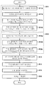
도 2는, 투영 광학계의 수차의 평가 방법 및 노광 방법을 도시하는 흐름도이다.
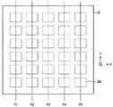
도 3a, 도 3b는, 평가용 마스크를 도시하는 도면이다.
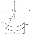
도 4는, 선 폭과 기판의 높이의 관계를 도시하는 도면이다.
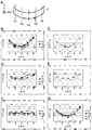
도 5의 A 내지 도 5의 G는, 투영 광학계의 수차를 평가하기 위하여 얻어진 특성을 도시하는 도면이다.
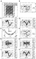
도 6의 A 내지 도 6의 J는, 투영 광학계의 수차를 평가하기 위하여 얻어진 특성을 도시하는 도면이다.
도 7은, 조명 조건의 변경을 수반하는 투영 광학계의 수차의 평가 방법 및 노광 방법을 도시하는 흐름도이다.







Claims (14)
- 노광 장치에 있어서의 투영 광학계의 수차를 평가하는 평가 방법이며,
마스크의 복수의 패턴 요소를 상기 노광 장치의 상기 투영 광학계에 의해 기판에 전사하는 전사 공정과,
상기 투영 광학계에 의한 상기 복수의 패턴 요소의 각각의 투영 위치에 관한 제1 특성값을 상기 전사 공정에서의 전사 결과에 기초하여 구하고, 상기 복수의 패턴 요소의 상기 제1 특성값의 평균값을 상기 투영 광학계의 수차를 나타내는 제1 정보로서 구하는 제1 공정과,
상기 투영 광학계에 의해 투영된 상기 복수의 패턴 요소의 상을 검출하는 검출 공정과,
상기 투영 광학계에 의한 상기 복수의 패턴 요소의 각각의 투영 위치에 관한 제2 특성값을 상기 검출 공정에서의 검출 결과에 기초하여 구하고, 상기 복수의 패턴 요소의 상기 제2 특성값의 평균값, 및 상기 복수의 패턴 요소의 각각에 관한 상기 제2 특성값과 상기 제2 특성값의 평균값의 차를 상기 투영 광학계의 수차를 나타내는 제2 정보로서 구하는 제2 공정과,
상기 제1 정보와 상기 제2 정보에 기초하여, 상기 투영 광학계의 수차를 평가하는 평가 공정을 포함하는 것을 특징으로 하는, 평가 방법. - 제1항에 있어서,
상기 평가 공정에서는, 상기 제2 특성값의 평균값을 상기 제1 특성값의 평균값으로 보정하여 얻어지는 상기 제2 정보에 기초하여, 상기 투영 광학계의 수차를 평가하는 것을 특징으로 하는, 평가 방법. - 제1항에 있어서,
상기 복수의 패턴 요소는, 라인이 신장되는 방향이 서로 상이한 복수의 라인 요소를 각각 포함하는 것을 특징으로 하는, 평가 방법. - 제3항에 있어서,
상기 복수의 라인 요소는, 라인이 신장되는 방향이 서로 45도씩 상이한 것을 특징으로 하는, 평가 방법. - 제3항에 있어서,
상기 제1 공정에서는, 라인이 신장되는 방향에 따라서 각 패턴 요소의 상기 제1 특성값에 가중치 부여하고, 상기 복수의 패턴 요소에 대하여 가중치 부여된 상기 제1 특성값의 평균값을 상기 제1 정보로서 구하는 것을 특징으로 하는, 평가 방법. - 제1항에 있어서,
상기 제1 특성값 및 상기 제2 특성값의 각각은, 상기 투영 광학계의 포커스값을 포함하고,
상기 평가 공정에서는, 상기 투영 광학계의 상면 만곡 및 비점 수차 중 적어도 한쪽을 평가하는 것을 특징으로 하는, 평가 방법. - 제1항에 있어서,
상기 제1 특성값 및 상기 제2 특성값의 각각은, 상기 투영 광학계의 광축과 수직인 방향에 있어서 상기 투영 광학계에 의해 상기 복수의 패턴 요소의 각각이 결상되는 위치와 목표 위치의 어긋남량을 포함하고,
상기 평가 공정에서는, 상기 투영 광학계의 왜곡 수차를 평가하는 것을 특징으로 하는, 평가 방법. - 제7항에 있어서,
상기 제1 특성값 및 상기 제2 특성값의 각각은, 상기 광축에 수직한 제1 방향에 있어서의 상기 어긋남량과, 상기 광축에 수직 또한 상기 제1 방향과 상이한 제2 방향에 있어서의 상기 어긋남량을 포함하는 것을 특징으로 하는, 평가 방법. - 제1항에 있어서,
상기 전사 공정은 1회만 행하여지는 것을 특징으로 하는, 평가 방법. - 제9항에 있어서,
상기 검출 공정은 복수 회 행해지고,
상기 제2 공정에서는, 복수 회의 상기 검출 공정에서 얻어진 복수의 검출 결과를 평균화한 결과에 기초하여 상기 제2 정보를 구하는 것을 특징으로 하는, 평가 방법. - 제1항에 있어서,
상기 노광 장치의 조명 조건이 변경된 경우,
변경 후의 조명 조건에서 상기 검출 공정 및 상기 제2 공정을 새롭게 행함으로써 변경 후의 조명 조건에서의 상기 제2 특성값을 구하고, 변경 후의 조명 조건에서의 상기 제2 특성값으로부터 상기 투영 광학계의 수차를 나타내는 제3 정보를 구하는 공정과,
변경 전의 조명 조건에서 구해진 상기 제2 정보와, 변경 후의 조명 조건에서 구해진 상기 제3 정보의 차에 기초하여, 변경 전의 조명 조건에서 구해진 상기 제1 정보를 보정하는 공정과,
보정한 상기 제1 정보에 의해 상기 제3 정보를 보정한 결과에 기초하여, 변경 후의 조명 조건에서의 상기 투영 광학계의 수차를 평가하는 공정을 행하는 것을 특징으로 하는, 평가 방법. - 기판을 노광하는 노광 방법이며,
제1항에 기재된 평가 방법을 사용하여 투영 광학계의 수차를 평가하는 공정과,
상기 투영 광학계의 수차의 평가 결과에 기초하여 상기 노광 장치를 교정하는 공정과,
교정된 상기 노광 장치를 사용하여 상기 기판을 노광하는 공정을 포함하는 것을 특징으로 하는, 노광 방법. - 제12항에 기재된 노광 방법을 사용하여 기판을 노광하는 공정과,
상기 공정에서 노광이 행하여진 상기 기판을 현상하는 공정을 포함하는 것을 특징으로 하는, 물품의 제조 방법. - 노광 장치에 있어서의 투영 광학계의 수차를 평가하는 평가 방법이며,
상기 투영 광학계에 의한 마스크의 복수의 패턴 요소의 각각의 투영 위치에 관한 제1 특성값을, 상기 복수의 패턴 요소를 상기 노광 장치의 상기 투영 광학계에 의해 기판에 전사한 전사 결과에 기초하여 구하고, 상기 복수의 패턴 요소의 상기 제1 특성값의 평균값을 상기 투영 광학계의 수차를 나타내는 제1 정보로서 구하는 제1 공정과,
상기 투영 광학계에 의한 상기 복수의 패턴 요소의 각각의 투영 위치에 관한 제2 특성값을, 상기 투영 광학계에 의해 투영된 상기 복수의 패턴 요소의 상을 검출한 검출 결과에 기초하여 구하고, 상기 복수의 패턴 요소의 상기 제2 특성값의 평균값, 및 상기 복수의 패턴 요소의 각각에 관한 상기 제2 특성값과 상기 제2 특성값의 평균값의 차를 상기 투영 광학계의 수차를 나타내는 제2 정보로서 구하는 제2 공정과,
상기 제1 정보와 상기 제2 정보에 기초하여, 상기 투영 광학계의 수차를 평가하는 평가 공정을 포함하는 것을 특징으로 하는, 평가 방법.
Applications Claiming Priority (2)
| Application Number | Priority Date | Filing Date | Title |
|---|---|---|---|
| JP2015254866A JP6661371B2 (ja) | 2015-12-25 | 2015-12-25 | 評価方法、露光方法、および物品の製造方法 |
| JPJP-P-2015-254866 | 2015-12-25 |
Publications (2)
| Publication Number | Publication Date |
|---|---|
| KR20170077041A true KR20170077041A (ko) | 2017-07-05 |
| KR102126232B1 KR102126232B1 (ko) | 2020-06-24 |
Family
ID=59234097
Family Applications (1)
| Application Number | Title | Priority Date | Filing Date |
|---|---|---|---|
| KR1020160172663A Active KR102126232B1 (ko) | 2015-12-25 | 2016-12-16 | 평가 방법, 노광 방법, 및 물품의 제조 방법 |
Country Status (4)
| Country | Link |
|---|---|
| JP (1) | JP6661371B2 (ko) |
| KR (1) | KR102126232B1 (ko) |
| CN (1) | CN106919004B (ko) |
| TW (1) | TWI643029B (ko) |
Families Citing this family (4)
| Publication number | Priority date | Publication date | Assignee | Title |
|---|---|---|---|---|
| JP6978926B2 (ja) * | 2017-12-18 | 2021-12-08 | キヤノン株式会社 | 計測方法、計測装置、露光装置、および物品製造方法 |
| JP7105582B2 (ja) * | 2018-03-09 | 2022-07-25 | キヤノン株式会社 | 決定方法、露光方法、露光装置、物品の製造方法及びプログラム |
| JP7357488B2 (ja) * | 2019-09-04 | 2023-10-06 | キヤノン株式会社 | 露光装置、および物品製造方法 |
| WO2025149231A1 (en) * | 2024-01-11 | 2025-07-17 | Asml Netherlands B.V. | Improvements to lithographic methods and apparatus |
Citations (6)
| Publication number | Priority date | Publication date | Assignee | Title |
|---|---|---|---|---|
| JPH10284414A (ja) * | 1997-04-10 | 1998-10-23 | Nikon Corp | 結像位置検出装置及び半導体デバイスの製造方法 |
| JPH11260703A (ja) * | 1998-03-16 | 1999-09-24 | Sony Corp | 露光装置および露光装置の投影レンズの評価方法 |
| JP2001166497A (ja) | 1999-10-01 | 2001-06-22 | Nikon Corp | 露光方法及び露光装置 |
| WO2002050506A1 (en) * | 2000-12-18 | 2002-06-27 | Nikon Corporation | Wavefront measuring apparatus and its usage, method and apparatus for determining focusing characteristics, method and apparatus for correcting focusing characteristics, method for managing focusing characteristics, and method and apparatus for exposure |
| JP2003215423A (ja) | 2002-01-28 | 2003-07-30 | Nikon Corp | 光学系の製造方法,投影光学装置および露光装置 |
| JP2004319397A (ja) * | 2003-04-18 | 2004-11-11 | Toyota Motor Corp | 車両用赤外線映像装置及びハイビームヘッドランプ構造 |
Family Cites Families (18)
| Publication number | Priority date | Publication date | Assignee | Title |
|---|---|---|---|---|
| JPH068926B2 (ja) * | 1984-08-24 | 1994-02-02 | キヤノン株式会社 | 面位置検出方法 |
| JPH02157844A (ja) * | 1988-12-12 | 1990-06-18 | Nikon Corp | 露光条件測定用マスク並びに該マスクを用いた露光条件測定方法及び装置 |
| JP3013463B2 (ja) * | 1991-02-01 | 2000-02-28 | 株式会社ニコン | 焦点位置検出装置及び投影露光装置 |
| JP2002022609A (ja) * | 2000-07-10 | 2002-01-23 | Canon Inc | 投影露光装置 |
| JP2003037052A (ja) * | 2001-07-26 | 2003-02-07 | Canon Inc | 投影光学系の収差測定手段を有する半導体露光装置 |
| US6778275B2 (en) * | 2002-02-20 | 2004-08-17 | Micron Technology, Inc. | Aberration mark and method for estimating overlay error and optical aberrations |
| US6897940B2 (en) * | 2002-06-21 | 2005-05-24 | Nikon Corporation | System for correcting aberrations and distortions in EUV lithography |
| JP2004319937A (ja) * | 2003-04-21 | 2004-11-11 | Nikon Corp | 計測方法、光学特性計測方法、露光装置の調整方法及び露光方法、並びにデバイス製造方法 |
| US7158215B2 (en) * | 2003-06-30 | 2007-01-02 | Asml Holding N.V. | Large field of view protection optical system with aberration correctability for flat panel displays |
| US7242475B2 (en) * | 2004-03-25 | 2007-07-10 | Asml Netherlands B.V. | Method of determining aberration of a projection system of a lithographic apparatus |
| CN1312464C (zh) * | 2004-04-29 | 2007-04-25 | 上海微电子装备有限公司 | 成像光学系统像差的现场测量方法 |
| CN101174092B (zh) * | 2006-10-30 | 2010-10-06 | 上海华虹Nec电子有限公司 | 用于监控镜头慧差导致成像畸变的方法及其透镜成像系统 |
| CN101221372A (zh) * | 2008-01-25 | 2008-07-16 | 中国科学院上海光学精密机械研究所 | 光刻机投影物镜偶像差原位检测系统及检测方法 |
| CN101236362B (zh) * | 2008-01-29 | 2010-06-23 | 北京理工大学 | 光刻机投影物镜波像差在线检测方法 |
| CN101464637B (zh) * | 2008-12-30 | 2011-03-30 | 上海微电子装备有限公司 | 光刻机投影物镜波像差测量装置及方法 |
| US8760624B2 (en) * | 2010-07-16 | 2014-06-24 | Rudolph Technologies, Inc. | System and method for estimating field curvature |
| US8760625B2 (en) * | 2010-07-30 | 2014-06-24 | Asml Netherlands B.V. | Lithographic apparatus, aberration detector and device manufacturing method |
| CN102681358B (zh) * | 2012-04-18 | 2014-02-12 | 中国科学院上海光学精密机械研究所 | 基于空间像检测的投影物镜波像差原位测量方法 |
-
2015
- 2015-12-25 JP JP2015254866A patent/JP6661371B2/ja active Active
-
2016
- 2016-11-04 TW TW105135975A patent/TWI643029B/zh active
- 2016-12-16 KR KR1020160172663A patent/KR102126232B1/ko active Active
- 2016-12-20 CN CN201611180236.3A patent/CN106919004B/zh active Active
Patent Citations (6)
| Publication number | Priority date | Publication date | Assignee | Title |
|---|---|---|---|---|
| JPH10284414A (ja) * | 1997-04-10 | 1998-10-23 | Nikon Corp | 結像位置検出装置及び半導体デバイスの製造方法 |
| JPH11260703A (ja) * | 1998-03-16 | 1999-09-24 | Sony Corp | 露光装置および露光装置の投影レンズの評価方法 |
| JP2001166497A (ja) | 1999-10-01 | 2001-06-22 | Nikon Corp | 露光方法及び露光装置 |
| WO2002050506A1 (en) * | 2000-12-18 | 2002-06-27 | Nikon Corporation | Wavefront measuring apparatus and its usage, method and apparatus for determining focusing characteristics, method and apparatus for correcting focusing characteristics, method for managing focusing characteristics, and method and apparatus for exposure |
| JP2003215423A (ja) | 2002-01-28 | 2003-07-30 | Nikon Corp | 光学系の製造方法,投影光学装置および露光装置 |
| JP2004319397A (ja) * | 2003-04-18 | 2004-11-11 | Toyota Motor Corp | 車両用赤外線映像装置及びハイビームヘッドランプ構造 |
Also Published As
| Publication number | Publication date |
|---|---|
| JP2017116867A (ja) | 2017-06-29 |
| CN106919004A (zh) | 2017-07-04 |
| TW201723678A (zh) | 2017-07-01 |
| TWI643029B (zh) | 2018-12-01 |
| KR102126232B1 (ko) | 2020-06-24 |
| CN106919004B (zh) | 2019-11-26 |
| JP6661371B2 (ja) | 2020-03-11 |
Similar Documents
| Publication | Publication Date | Title |
|---|---|---|
| US10545413B2 (en) | Evaluation method, exposure method, and method for manufacturing an article | |
| US10234775B2 (en) | Exposure apparatus, exposure method, and method of manufacturing article | |
| JP6917477B2 (ja) | リソグラフィ装置及びリソグラフィ方法 | |
| US20090220872A1 (en) | Detecting apparatus, exposure apparatus, and device manufacturing method | |
| KR102396135B1 (ko) | 계산 방법, 노광 방법, 기억 매체, 노광 장치 및 물품 제조 방법 | |
| KR102126232B1 (ko) | 평가 방법, 노광 방법, 및 물품의 제조 방법 | |
| CN109634054B (zh) | 校正半导体光刻的光掩模的临界尺寸均匀性的方法 | |
| KR20230047898A (ko) | 기판상의 복수의 숏 영역의 배열을 구하는 방법, 노광 방법, 노광 장치, 물품의 제조 방법, 비일시적 컴퓨터 판독 가능한 기억 매체, 및 정보처리장치 | |
| US9996916B2 (en) | Evaluation method, storage medium, exposure apparatus, exposure method, and method of manufacturing article | |
| TW201827946A (zh) | 監測來自度量衡裝置之照明特性的方法 | |
| KR102242152B1 (ko) | 리소그래피 장치 및 물품 제조 방법 | |
| KR101320240B1 (ko) | 파면수차 측정 장치, 노광 장치 및 디바이스 제조 방법 | |
| KR102877760B1 (ko) | 국부 균일성 메트릭을 추론하는 방법 | |
| US8077290B2 (en) | Exposure apparatus, and device manufacturing method | |
| KR102809336B1 (ko) | 마크 위치 결정 방법, 리소그래피 방법, 물품제조방법, 프로그램 및 리소그래피 장치 | |
| US10871718B2 (en) | Exposure apparatus, method for controlling the same and article manufacturing method | |
| JP2009047523A (ja) | 干渉測定装置、露光装置およびデバイス製造方法 | |
| JP7213757B2 (ja) | 露光装置、および物品製造方法 | |
| CN107870522B (zh) | 成像光路装置与成像光路装置的检测控制方法 | |
| JP6367021B2 (ja) | 露光条件解析方法 | |
| KR20180059944A (ko) | 토포그래피 측정 시스템 | |
| JP5922927B2 (ja) | 位置を求める方法、情報処理装置、リソグラフィ装置及び物品の製造方法 | |
| CN119225122A (zh) | 信息处理装置、信息处理方法、存储介质、曝光方法、基板处理装置以及物品的制造方法 | |
| TW202518183A (zh) | 測定物體表面位置的方法 | |
| JP2015176957A (ja) | 投影光学系のフォーカス特性の計測方法、及び計測装置 |
Legal Events
| Date | Code | Title | Description |
|---|---|---|---|
| PA0109 | Patent application |
Patent event code: PA01091R01D Comment text: Patent Application Patent event date: 20161216 |
|
| PG1501 | Laying open of application | ||
| A201 | Request for examination | ||
| PA0201 | Request for examination |
Patent event code: PA02012R01D Patent event date: 20180618 Comment text: Request for Examination of Application Patent event code: PA02011R01I Patent event date: 20161216 Comment text: Patent Application |
|
| E902 | Notification of reason for refusal | ||
| PE0902 | Notice of grounds for rejection |
Comment text: Notification of reason for refusal Patent event date: 20191209 Patent event code: PE09021S01D |
|
| E701 | Decision to grant or registration of patent right | ||
| PE0701 | Decision of registration |
Patent event code: PE07011S01D Comment text: Decision to Grant Registration Patent event date: 20200403 |
|
| GRNT | Written decision to grant | ||
| PR0701 | Registration of establishment |
Comment text: Registration of Establishment Patent event date: 20200618 Patent event code: PR07011E01D |
|
| PR1002 | Payment of registration fee |
Payment date: 20200619 End annual number: 3 Start annual number: 1 |
|
| PG1601 | Publication of registration | ||
| PR1001 | Payment of annual fee |
Payment date: 20240527 Start annual number: 5 End annual number: 5 |