KR20170077261A - Systems and methods for mems light modulator arrays with reduced acoustic emission - Google Patents
Systems and methods for mems light modulator arrays with reduced acoustic emission Download PDFInfo
- Publication number
- KR20170077261A KR20170077261A KR1020177017136A KR20177017136A KR20170077261A KR 20170077261 A KR20170077261 A KR 20170077261A KR 1020177017136 A KR1020177017136 A KR 1020177017136A KR 20177017136 A KR20177017136 A KR 20177017136A KR 20170077261 A KR20170077261 A KR 20170077261A
- Authority
- KR
- South Korea
- Prior art keywords
- optical modulators
- light
- array
- shutter
- groups
- Prior art date
- Legal status (The legal status is an assumption and is not a legal conclusion. Google has not performed a legal analysis and makes no representation as to the accuracy of the status listed.)
- Ceased
Links
- 238000000034 method Methods 0.000 title claims abstract description 65
- 238000003491 array Methods 0.000 title description 11
- 230000003287 optical effect Effects 0.000 claims abstract description 204
- 239000011159 matrix material Substances 0.000 claims abstract description 86
- 239000000758 substrate Substances 0.000 claims abstract description 66
- 230000033001 locomotion Effects 0.000 claims description 59
- 230000000977 initiatory effect Effects 0.000 claims description 6
- 238000004519 manufacturing process Methods 0.000 claims description 6
- 230000008878 coupling Effects 0.000 claims description 2
- 238000010168 coupling process Methods 0.000 claims description 2
- 238000005859 coupling reaction Methods 0.000 claims description 2
- 230000000712 assembly Effects 0.000 description 30
- 238000000429 assembly Methods 0.000 description 30
- 239000003990 capacitor Substances 0.000 description 21
- 239000003086 colorant Substances 0.000 description 12
- 238000013500 data storage Methods 0.000 description 12
- 239000012530 fluid Substances 0.000 description 10
- 230000006870 function Effects 0.000 description 10
- 239000000463 material Substances 0.000 description 10
- 239000010408 film Substances 0.000 description 9
- 238000005286 illumination Methods 0.000 description 9
- 239000011521 glass Substances 0.000 description 8
- 230000008569 process Effects 0.000 description 8
- 239000004033 plastic Substances 0.000 description 7
- 239000010409 thin film Substances 0.000 description 7
- 230000004044 response Effects 0.000 description 6
- 230000000903 blocking effect Effects 0.000 description 5
- 238000010586 diagram Methods 0.000 description 5
- 238000003384 imaging method Methods 0.000 description 5
- 241001270131 Agaricus moelleri Species 0.000 description 4
- 239000011358 absorbing material Substances 0.000 description 4
- 230000000295 complement effect Effects 0.000 description 4
- 238000013461 design Methods 0.000 description 4
- 230000003071 parasitic effect Effects 0.000 description 4
- 230000005534 acoustic noise Effects 0.000 description 3
- 239000006227 byproduct Substances 0.000 description 3
- 230000015556 catabolic process Effects 0.000 description 3
- 238000006073 displacement reaction Methods 0.000 description 3
- 230000009977 dual effect Effects 0.000 description 3
- 239000004973 liquid crystal related substance Substances 0.000 description 3
- 239000002184 metal Substances 0.000 description 3
- 238000012545 processing Methods 0.000 description 3
- 238000012163 sequencing technique Methods 0.000 description 3
- 239000007787 solid Substances 0.000 description 3
- 125000006850 spacer group Chemical group 0.000 description 3
- XUIMIQQOPSSXEZ-UHFFFAOYSA-N Silicon Chemical compound [Si] XUIMIQQOPSSXEZ-UHFFFAOYSA-N 0.000 description 2
- 230000003044 adaptive effect Effects 0.000 description 2
- 239000000853 adhesive Substances 0.000 description 2
- 230000001070 adhesive effect Effects 0.000 description 2
- 230000008901 benefit Effects 0.000 description 2
- 230000005540 biological transmission Effects 0.000 description 2
- 230000007613 environmental effect Effects 0.000 description 2
- 238000005530 etching Methods 0.000 description 2
- 238000012423 maintenance Methods 0.000 description 2
- 238000005459 micromachining Methods 0.000 description 2
- 238000011022 operating instruction Methods 0.000 description 2
- 239000000565 sealant Substances 0.000 description 2
- 229910052710 silicon Inorganic materials 0.000 description 2
- 239000010703 silicon Substances 0.000 description 2
- 230000002123 temporal effect Effects 0.000 description 2
- 230000000007 visual effect Effects 0.000 description 2
- 239000004593 Epoxy Substances 0.000 description 1
- 230000003213 activating effect Effects 0.000 description 1
- WYTGDNHDOZPMIW-RCBQFDQVSA-N alstonine Natural products C1=CC2=C3C=CC=CC3=NC2=C2N1C[C@H]1[C@H](C)OC=C(C(=O)OC)[C@H]1C2 WYTGDNHDOZPMIW-RCBQFDQVSA-N 0.000 description 1
- 229910021417 amorphous silicon Inorganic materials 0.000 description 1
- 230000006399 behavior Effects 0.000 description 1
- 230000015572 biosynthetic process Effects 0.000 description 1
- 210000004556 brain Anatomy 0.000 description 1
- 230000008859 change Effects 0.000 description 1
- 238000005229 chemical vapour deposition Methods 0.000 description 1
- 150000001875 compounds Chemical class 0.000 description 1
- 238000010276 construction Methods 0.000 description 1
- 238000007599 discharging Methods 0.000 description 1
- 230000000694 effects Effects 0.000 description 1
- 238000005516 engineering process Methods 0.000 description 1
- 238000001704 evaporation Methods 0.000 description 1
- 230000008020 evaporation Effects 0.000 description 1
- 238000010237 hybrid technique Methods 0.000 description 1
- 230000002209 hydrophobic effect Effects 0.000 description 1
- 239000007924 injection Substances 0.000 description 1
- 238000002347 injection Methods 0.000 description 1
- 238000007689 inspection Methods 0.000 description 1
- 238000007733 ion plating Methods 0.000 description 1
- 230000001788 irregular Effects 0.000 description 1
- 238000000608 laser ablation Methods 0.000 description 1
- 238000001182 laser chemical vapour deposition Methods 0.000 description 1
- 239000007788 liquid Substances 0.000 description 1
- 239000000314 lubricant Substances 0.000 description 1
- 230000000873 masking effect Effects 0.000 description 1
- 230000007246 mechanism Effects 0.000 description 1
- 238000001393 microlithography Methods 0.000 description 1
- 239000002991 molded plastic Substances 0.000 description 1
- 230000008447 perception Effects 0.000 description 1
- 230000000737 periodic effect Effects 0.000 description 1
- 238000004382 potting Methods 0.000 description 1
- 238000007781 pre-processing Methods 0.000 description 1
- 238000004886 process control Methods 0.000 description 1
- 238000004064 recycling Methods 0.000 description 1
- 230000000284 resting effect Effects 0.000 description 1
- 239000004065 semiconductor Substances 0.000 description 1
- 238000010008 shearing Methods 0.000 description 1
- 238000004544 sputter deposition Methods 0.000 description 1
- 238000003860 storage Methods 0.000 description 1
- 230000001360 synchronised effect Effects 0.000 description 1
- 238000012360 testing method Methods 0.000 description 1
- 230000001052 transient effect Effects 0.000 description 1
- 239000012780 transparent material Substances 0.000 description 1
- 238000007740 vapor deposition Methods 0.000 description 1
- 238000009736 wetting Methods 0.000 description 1
Images






Classifications
-
- G—PHYSICS
- G09—EDUCATION; CRYPTOGRAPHY; DISPLAY; ADVERTISING; SEALS
- G09G—ARRANGEMENTS OR CIRCUITS FOR CONTROL OF INDICATING DEVICES USING STATIC MEANS TO PRESENT VARIABLE INFORMATION
- G09G3/00—Control arrangements or circuits, of interest only in connection with visual indicators other than cathode-ray tubes
- G09G3/20—Control arrangements or circuits, of interest only in connection with visual indicators other than cathode-ray tubes for presentation of an assembly of a number of characters, e.g. a page, by composing the assembly by combination of individual elements arranged in a matrix no fixed position being assigned to or needed to be assigned to the individual characters or partial characters
- G09G3/34—Control arrangements or circuits, of interest only in connection with visual indicators other than cathode-ray tubes for presentation of an assembly of a number of characters, e.g. a page, by composing the assembly by combination of individual elements arranged in a matrix no fixed position being assigned to or needed to be assigned to the individual characters or partial characters by control of light from an independent source
- G09G3/3433—Control arrangements or circuits, of interest only in connection with visual indicators other than cathode-ray tubes for presentation of an assembly of a number of characters, e.g. a page, by composing the assembly by combination of individual elements arranged in a matrix no fixed position being assigned to or needed to be assigned to the individual characters or partial characters by control of light from an independent source using light modulating elements actuated by an electric field and being other than liquid crystal devices and electrochromic devices
-
- G—PHYSICS
- G02—OPTICS
- G02B—OPTICAL ELEMENTS, SYSTEMS OR APPARATUS
- G02B26/00—Optical devices or arrangements for the control of light using movable or deformable optical elements
- G02B26/02—Optical devices or arrangements for the control of light using movable or deformable optical elements for controlling the intensity of light
- G02B26/04—Optical devices or arrangements for the control of light using movable or deformable optical elements for controlling the intensity of light by periodically varying the intensity of light, e.g. using choppers
-
- G—PHYSICS
- G02—OPTICS
- G02B—OPTICAL ELEMENTS, SYSTEMS OR APPARATUS
- G02B26/00—Optical devices or arrangements for the control of light using movable or deformable optical elements
- G02B26/02—Optical devices or arrangements for the control of light using movable or deformable optical elements for controlling the intensity of light
-
- G—PHYSICS
- G09—EDUCATION; CRYPTOGRAPHY; DISPLAY; ADVERTISING; SEALS
- G09G—ARRANGEMENTS OR CIRCUITS FOR CONTROL OF INDICATING DEVICES USING STATIC MEANS TO PRESENT VARIABLE INFORMATION
- G09G2300/00—Aspects of the constitution of display devices
- G09G2300/04—Structural and physical details of display devices
- G09G2300/0439—Pixel structures
- G09G2300/0456—Pixel structures with a reflective area and a transmissive area combined in one pixel, such as in transflectance pixels
-
- G—PHYSICS
- G09—EDUCATION; CRYPTOGRAPHY; DISPLAY; ADVERTISING; SEALS
- G09G—ARRANGEMENTS OR CIRCUITS FOR CONTROL OF INDICATING DEVICES USING STATIC MEANS TO PRESENT VARIABLE INFORMATION
- G09G2300/00—Aspects of the constitution of display devices
- G09G2300/08—Active matrix structure, i.e. with use of active elements, inclusive of non-linear two terminal elements, in the pixels together with light emitting or modulating elements
- G09G2300/0809—Several active elements per pixel in active matrix panels
- G09G2300/0842—Several active elements per pixel in active matrix panels forming a memory circuit, e.g. a dynamic memory with one capacitor
-
- G—PHYSICS
- G09—EDUCATION; CRYPTOGRAPHY; DISPLAY; ADVERTISING; SEALS
- G09G—ARRANGEMENTS OR CIRCUITS FOR CONTROL OF INDICATING DEVICES USING STATIC MEANS TO PRESENT VARIABLE INFORMATION
- G09G2300/00—Aspects of the constitution of display devices
- G09G2300/08—Active matrix structure, i.e. with use of active elements, inclusive of non-linear two terminal elements, in the pixels together with light emitting or modulating elements
- G09G2300/0809—Several active elements per pixel in active matrix panels
- G09G2300/0842—Several active elements per pixel in active matrix panels forming a memory circuit, e.g. a dynamic memory with one capacitor
- G09G2300/0857—Static memory circuit, e.g. flip-flop
-
- G—PHYSICS
- G09—EDUCATION; CRYPTOGRAPHY; DISPLAY; ADVERTISING; SEALS
- G09G—ARRANGEMENTS OR CIRCUITS FOR CONTROL OF INDICATING DEVICES USING STATIC MEANS TO PRESENT VARIABLE INFORMATION
- G09G2310/00—Command of the display device
- G09G2310/02—Addressing, scanning or driving the display screen or processing steps related thereto
- G09G2310/0235—Field-sequential colour display
-
- G—PHYSICS
- G09—EDUCATION; CRYPTOGRAPHY; DISPLAY; ADVERTISING; SEALS
- G09G—ARRANGEMENTS OR CIRCUITS FOR CONTROL OF INDICATING DEVICES USING STATIC MEANS TO PRESENT VARIABLE INFORMATION
- G09G2310/00—Command of the display device
- G09G2310/02—Addressing, scanning or driving the display screen or processing steps related thereto
- G09G2310/0243—Details of the generation of driving signals
- G09G2310/0251—Precharge or discharge of pixel before applying new pixel voltage
-
- G—PHYSICS
- G09—EDUCATION; CRYPTOGRAPHY; DISPLAY; ADVERTISING; SEALS
- G09G—ARRANGEMENTS OR CIRCUITS FOR CONTROL OF INDICATING DEVICES USING STATIC MEANS TO PRESENT VARIABLE INFORMATION
- G09G2310/00—Command of the display device
- G09G2310/02—Addressing, scanning or driving the display screen or processing steps related thereto
- G09G2310/0262—The addressing of the pixel, in a display other than an active matrix LCD, involving the control of two or more scan electrodes or two or more data electrodes, e.g. pixel voltage dependent on signals of two data electrodes
-
- G—PHYSICS
- G09—EDUCATION; CRYPTOGRAPHY; DISPLAY; ADVERTISING; SEALS
- G09G—ARRANGEMENTS OR CIRCUITS FOR CONTROL OF INDICATING DEVICES USING STATIC MEANS TO PRESENT VARIABLE INFORMATION
- G09G2310/00—Command of the display device
- G09G2310/08—Details of timing specific for flat panels, other than clock recovery
-
- G—PHYSICS
- G09—EDUCATION; CRYPTOGRAPHY; DISPLAY; ADVERTISING; SEALS
- G09G—ARRANGEMENTS OR CIRCUITS FOR CONTROL OF INDICATING DEVICES USING STATIC MEANS TO PRESENT VARIABLE INFORMATION
- G09G2320/00—Control of display operating conditions
- G09G2320/04—Maintaining the quality of display appearance
- G09G2320/041—Temperature compensation
-
- G—PHYSICS
- G09—EDUCATION; CRYPTOGRAPHY; DISPLAY; ADVERTISING; SEALS
- G09G—ARRANGEMENTS OR CIRCUITS FOR CONTROL OF INDICATING DEVICES USING STATIC MEANS TO PRESENT VARIABLE INFORMATION
- G09G2320/00—Control of display operating conditions
- G09G2320/06—Adjustment of display parameters
- G09G2320/0626—Adjustment of display parameters for control of overall brightness
-
- G—PHYSICS
- G09—EDUCATION; CRYPTOGRAPHY; DISPLAY; ADVERTISING; SEALS
- G09G—ARRANGEMENTS OR CIRCUITS FOR CONTROL OF INDICATING DEVICES USING STATIC MEANS TO PRESENT VARIABLE INFORMATION
- G09G2360/00—Aspects of the architecture of display systems
- G09G2360/14—Detecting light within display terminals, e.g. using a single or a plurality of photosensors
- G09G2360/144—Detecting light within display terminals, e.g. using a single or a plurality of photosensors the light being ambient light
-
- G—PHYSICS
- G09—EDUCATION; CRYPTOGRAPHY; DISPLAY; ADVERTISING; SEALS
- G09G—ARRANGEMENTS OR CIRCUITS FOR CONTROL OF INDICATING DEVICES USING STATIC MEANS TO PRESENT VARIABLE INFORMATION
- G09G3/00—Control arrangements or circuits, of interest only in connection with visual indicators other than cathode-ray tubes
- G09G3/20—Control arrangements or circuits, of interest only in connection with visual indicators other than cathode-ray tubes for presentation of an assembly of a number of characters, e.g. a page, by composing the assembly by combination of individual elements arranged in a matrix no fixed position being assigned to or needed to be assigned to the individual characters or partial characters
- G09G3/34—Control arrangements or circuits, of interest only in connection with visual indicators other than cathode-ray tubes for presentation of an assembly of a number of characters, e.g. a page, by composing the assembly by combination of individual elements arranged in a matrix no fixed position being assigned to or needed to be assigned to the individual characters or partial characters by control of light from an independent source
- G09G3/3406—Control of illumination source
- G09G3/3413—Details of control of colour illumination sources
-
- Y—GENERAL TAGGING OF NEW TECHNOLOGICAL DEVELOPMENTS; GENERAL TAGGING OF CROSS-SECTIONAL TECHNOLOGIES SPANNING OVER SEVERAL SECTIONS OF THE IPC; TECHNICAL SUBJECTS COVERED BY FORMER USPC CROSS-REFERENCE ART COLLECTIONS [XRACs] AND DIGESTS
- Y10—TECHNICAL SUBJECTS COVERED BY FORMER USPC
- Y10T—TECHNICAL SUBJECTS COVERED BY FORMER US CLASSIFICATION
- Y10T29/00—Metal working
- Y10T29/49—Method of mechanical manufacture
- Y10T29/49002—Electrical device making
Landscapes
- Physics & Mathematics (AREA)
- General Physics & Mathematics (AREA)
- Engineering & Computer Science (AREA)
- Optics & Photonics (AREA)
- Computer Hardware Design (AREA)
- Theoretical Computer Science (AREA)
- Mechanical Light Control Or Optical Switches (AREA)
- Micromachines (AREA)
Abstract
픽셀들의 어레이, 기판, 및 기판 상에 형성된 제어 매트릭스를 갖는 디스플레이를 위한 시스템들 및 방법들이 설명된다. 픽셀들의 어레이는 마이크로-전기-기계적 또는 MEMS 광 변조기들로서 지칭될 수 있는 기계적 광 변조기들을 포함한다. MEMS 광 변조기들은 셔터-기반의 광 변조기들일 수도 있으며, 애퍼쳐들의 어레이는 기판 상에 셔터-기반의 광 변조기들의 어레이에서의 셔터들에 공간 대응하여 형성될 수도 있다. 각각의 변조기는 이동 방향을 통해서 광-차단 상태로부터 광-투과 상태로 구동되도록 구성된다. 광 변조기들의 어레이는 이웃하는 픽셀들의 이동 방향들에서의 상관 관계들을 감소시켜 디스플레이로부터의 음향 방출들의 진폭을 감소시키도록 배열된다.Systems and methods for a display having an array of pixels, a substrate, and a control matrix formed on the substrate are described. The array of pixels includes mechanical light modulators, which can be referred to as micro-electro-mechanical or MEMS optical modulators. The MEMS optical modulators may be shutter-based optical modulators, and the array of apertures may be formed in a space corresponding to the shutters in the array of shutter-based optical modulators on the substrate. Each modulator is configured to be driven from the light-shielding state to the light-transmitting state through the moving direction. The array of light modulators is arranged to reduce correlations in the moving directions of neighboring pixels to reduce the amplitude of acoustic emissions from the display.
Description
일반적으로, 본 출원은 이미징 디스플레이들에의 그들의 응용을 포함한, 광 변조 어레이들의 분야에 관한 것이다. 특히, 본 출원은 감소된 음향 방출 및 가청 잡음으로 동작하도록 설계된 광 변조기 어레이들에 관한 것이다.In general, the present application relates to the field of light modulation arrays, including their application to imaging displays. In particular, the present application relates to optical modulator arrays designed to operate with reduced acoustic emissions and audible noise.
기계적 광 변조기 (mechanical light modulator) 들로 형성된 디스플레이들은 액정 기술에 기초한 디스플레이들에 대한 매력적인 대안이다. 기계적 광 변조기들은 비디오 콘텐츠를 우수한 시야각들로 그리고 넓은 범위의 칼라 및 그레이 스케일로 디스플레이하기에 충분히 빠르다. 기계적 광 변조기들은 투사형 디스플레이 애플리케이션들에서 성공적이었으며, 최근 직접 뷰 애플리케이션들 (direct view applications) 에 제안되고 있다.Displays formed with mechanical light modulators are an attractive alternative to displays based on liquid crystal technology. Mechanical optical modulators are fast enough to display video content at excellent viewing angles and in a wide range of colors and grayscales. Mechanical optical modulators have been successful in projection display applications and are currently being proposed in direct view applications.
기계적 광 변조기들로 형성된 다수의 디스플레이 프로토타입들은 최근에 제조되었지만, 이들 중 많은 것들은 바람직하지 않은 가청 잡음을 발생한다. 기계적 광 변조기들의 어레이로 형성된 디스플레이는 수만의 광 변조기들을, 디스플레이의 각각의 픽셀에 대해 적어도 하나를 포함할 수 있으며, 수백만 까지의 광 변조기들을 포함할 수 있다. 각각의 광 변조기의 모션은 종종 백플레인 회로 (backplane circuit) 로서 지칭되는, 제어 매트릭스를 통해서 지시되는 지령들에 의해 제어된다. 비디오 동작 동안, 개개의 광 변조기들의 동작 상태는 초당 50 회로부터 초당 50,000 회까지 변화될 수 있다. 그 결과, 수천의 셔터 어셈블리들이 가청 주파수들의 시간 스케일들 특성을 넘어서 이동하여, 디스플레이들이 바람직하지 않은 음향 잡음을 부산물로서 방출할 수 있다.Although many display prototypes formed of mechanical light modulators have been recently produced, many of them produce undesirable audible noise. A display formed of an array of mechanical light modulators may contain tens of thousands of optical modulators, at least one for each pixel of the display, and may include up to several million optical modulators. The motion of each optical modulator is controlled by commands indicated through a control matrix, often referred to as a backplane circuit. During video operation, the operating state of the individual optical modulators can vary from 50 cycles per second to 50,000 cycles per second. As a result, thousands of shutter assemblies move beyond the temporal scales of audible frequencies, allowing displays to emit undesirable acoustic noise as a by-product.
디스플레이 어셈블리에서 개개의 픽셀들은 종종 단지 수십 마이크론 내지 수백 마이크론의 사이즈이지만, 디스플레이에서 보통의 이미지들은 밀리미터들 또는 심지어 센티미터들일 수 있는 균일한 칼라 또는 콘트라스트의 영역들을 가질 수 있다. 따라서, 디스플레이의 이웃하는 영역에서 수십 또는 수백의 광 변조기들은 제어 매트릭스로부터의 신호들에 의해 유사한 모션들로 그리고 유사한 타이밍 신호들로 이동하도록 야기되는 것이 일상적인 일이다. 이웃하는 픽셀들의 이동들의 이 동기화 또는 상관은 음향 방출들의 진폭에 기여한다.Although individual pixels in a display assembly are often only a few tens of microns to a few hundred microns in size, ordinary images in a display can have uniform color or contrast areas that can be millimeters or even centimeters. Hence, it is usual for tens or hundreds of optical modulators in neighboring areas of the display to be caused to move in similar motions and similar timing signals by signals from the control matrix. This synchronization or correlation of movements of neighboring pixels contributes to the amplitude of the acoustic emissions.
따라서, 이웃하는 MEMS 광 변조기들의 이동 방향들에서 상관 관계들을 감소시켜 음향 방출들의 진폭을 감소시킬 수 있는, 광 변조기들의 어레이에 대한 설계들이 추구된다.Accordingly, designs are sought for arrays of optical modulators that can reduce correlations in the direction of movement of neighboring MEMS optical modulators to reduce the amplitude of acoustic emissions.
일 양태에 따르면, 본 개시물은 기판, 기판 상에 형성된 애퍼쳐들의 어레이, 및 애퍼쳐들의 어레이에 공간 대응하여 형성된 MEMS 광 변조기들의 어레이를 포함하는 디스플레이에 관한 것이다. MEMS 광 변조기들의 어레이는 제 1 방향으로의 이동을 통해서 광-차단 상태로부터 광-투과 상태로 구동되도록 구성된 변조기들의 제 1 그룹을 포함한다. 어레이는 제 2 방향으로의 이동을 통해서 광-차단 상태로부터 광-투과 상태로 구동되도록 구성된 MEMS 광 변조기들의 제 2 그룹을 더 포함한다. 제 2 방향은 제 1 방향과는 실질적으로 상이하다. 일 구현예에서, 기판은 투명하다.SUMMARY OF THE INVENTION In accordance with one aspect, the disclosure is directed to a display comprising an array of apertures formed on a substrate, an array of apertures formed on the substrate, and an array of MEMS optical modulators spatially corresponding to the array of apertures. The array of MEMS optical modulators includes a first group of modulators configured to be driven from a light-blocking state to a light-transmissive state through movement in a first direction. The array further includes a second group of MEMS optical modulators configured to be driven from the light-blocking state to the light-transmissive state through movement in a second direction. The second direction is substantially different from the first direction. In one embodiment, the substrate is transparent.
일부 구현예들에서, 제 1 방향 및 제 2 방향은 평면 반대 방향들이다. 대안적인 구현예들에서, 제 2 방향은 제 1 방향에 대해 약 90, 60, 또는 45 도 회전될 수 있다. 광 변조기들의 어레이는 또한 이웃하는 MEMS 광 변조기들의 이동 방향들에서의 상관 관계들을 감소시키도록 배열된다. 일 구현예에서, 제 1 및 제 2 그룹들의 광 변조기들은 교번하는 칼럼들의 그룹들에 배열되며, 여기서 각각의 그룹은 적어도 하나의 칼럼을 포함한다. 다른 구현예에서, 제 1 및 제 2 그룹들의 광 변조기들은 교번하는 로우들의 그룹들에 배열되며, 여기서 각각의 그룹은 하나 이상의 로우들을 포함한다. 여전히 다른 구현예에서, 제 1 및 제 2 그룹들의 광 변조기들은 교번하는 클러스터들에 배열되며, 여기서, 각각의 클러스터는 적어도 하나의 변조기를 포함한다. 일부 구현예들에서, 광 변조기들의 2개의 그룹들 사이의 교번하는 공간 기간은 대략 애퍼쳐들의 어레이를 갖는 기판의 두께 미만이다. 여전히 다른 구현예에서, 제 1 및 제 2 그룹들의 광 변조기들은 무작위 방식으로 배열된다.In some embodiments, the first direction and the second direction are opposite directions. In alternate embodiments, the second direction may be rotated about 90, 60, or 45 degrees relative to the first direction. The array of optical modulators is also arranged to reduce correlations in the moving directions of neighboring MEMS optical modulators. In one implementation, the first and second groups of optical modulators are arranged in groups of alternating columns, where each group comprises at least one column. In another embodiment, the first and second groups of optical modulators are arranged in groups of alternating rows, where each group comprises one or more rows. In still other embodiments, the first and second groups of optical modulators are arranged in alternating clusters, wherein each cluster includes at least one modulator. In some embodiments, the alternating spacing period between two groups of light modulators is less than the thickness of the substrate having an array of apertures. In still other embodiments, the first and second groups of optical modulators are arranged in a random manner.
일부 구현예들에서, MEMS 광 변조기들은 셔터-기반의 광 변조기들일 수도 있다. 일부 구현예들에서, 광 변조기들은 셔터가 대응하는 애퍼쳐로부터의 광을 완전히 차단하지 않는 제 3 상태를 포함할 수 있다.In some implementations, the MEMS optical modulators may be shutter-based optical modulators. In some implementations, the light modulators may include a third state in which the shutter does not completely block light from the corresponding aperture.
일부 구현예들에서, 디스플레이 장치는 데이터 및 작동 전압들 (actuation voltages) 을 어레이로 송신하기 위해 제 1 기판 상에 형성된 드라이버 칩 및 제어 매트릭스를 포함한다. 디스플레이 장치는 또한 이동의 제 1 및 제 2 방향들 중 어느 방향이 어레이에서의 각각의 광 변조기에 대해 광-투과 상태를 달성하기에 적당한 지를 메모리에 저장하는 제어기를 포함한다.In some embodiments, the display device includes a driver chip and a control matrix formed on the first substrate to transmit data and actuation voltages to the array. The display device also includes a controller for storing in memory one of the first and second directions of movement suitable for achieving a light-transmissive state for each light modulator in the array.
일부 구현예들에서, 제어 매트릭스는 2개의 그룹들을 실질적으로 상이한 방향들로 구동하기 위해 별개의 배선 레이아웃들 (wiring layouts) 로 구성된다. 대안적인 구현예들에서, 제어기는 활성 상태를 달성하기 위해 어레이에서의 광 변조기들의 제 1 및 제 2 그룹들의 맵 및 그들의 연관되는 이동의 방향을 메모리에 저장한다. 제어기는 각각의 픽셀에 대한 이동의 적당한 방향을 결정하기 위해, 제어 매트릭스를 통해서 전송하기 전에, 픽셀 데이터를 프로세싱한다.In some implementations, the control matrix consists of separate wiring layouts to drive the two groups in substantially different directions. In alternative embodiments, the controller stores the map of the first and second groups of optical modulators in the array and the direction of their associated movement in memory to achieve the active state. The controller processes the pixel data before sending it through the control matrix to determine the proper direction of movement for each pixel.
다른 양태에 따르면, 본 개시물은 디스플레이를 제조하는 방법에 관한 것이다. 이 방법은 기판 상에 애퍼쳐들의 어레이를 형성하는 단계, 및 MEMS 광 변조기들의 제 1 그룹에서의 광 변조기들이 제 1 방향으로의 이동을 통해서 광-차단 상태로부터 광-투과 상태로 작동하도록 구성되게, 기판 상에 애퍼쳐들의 어레이에 공간 대응하여 MEMS 광 변조기들의 제 1 그룹을 제조하는 단계를 포함한다. 이 방법은 MEMS 광 변조기들의 제 2 그룹에서의 광 변조기들이 제 2 방향으로의 이동을 통해서 광-차단 상태로부터 광-투과 상태로 작동하도록 구성되게, MEMS 광 변조기들의 제 2 그룹을 기판 상에 애퍼쳐들의 어레이에 공간 대응하여 제조하는 단계를 더 포함한다. 제 2 방향은 제 1 방향과는 실질적으로 상이하다.According to another aspect, the disclosure is directed to a method of manufacturing a display. The method comprises the steps of forming an array of apertures on a substrate and configuring the optical modulators in the first group of MEMS optical modulators to operate in a light-transmissive state from a light-interrupted state through movement in a first direction And fabricating a first group of MEMS light modulators on the substrate in a space corresponding to the array of apertures. The method includes positioning the second group of MEMS optical modulators on the substrate in such a way that the optical modulators in the second group of MEMS optical modulators are configured to operate in a light-transmissive state from the light- RTI ID = 0.0 > spatially < / RTI > The second direction is substantially different from the first direction.
다른 양태에 따르면, 본 개시물은 디스플레이 상에 이미지를 형성하기 위해 광을 변조하는 시스템에 관한 것이다. 시스템은 기판 상의 애퍼쳐들의 어레이 및 애퍼쳐들의 어레이에 공간 대응하여 배열된 MEMS 광 변조기들의 어레이를 포함한다. 시스템은 제 1 방향으로 MEMS 광 변조기들의 이동을 개시함으로써 MEMS 광 변조기들의 어레이에서의 MEMS 광 변조기들의 제 1 그룹을 광-차단 상태로부터 광-투과 상태로 작동하는 수단, 및 제 2 방향으로 MEMS 광 변조기들의 이동을 개시함으로써, MEMS 광 변조기들의 어레이에서의 MEMS 광 변조기들의 제 2 그룹을 광-차단 상태로부터 광-투과 상태로 작동하는 수단을 더 포함한다. 제 2 방향은 제 1 방향과는 실질적으로 상이하다.According to another aspect, the disclosure is directed to a system for modulating light to form an image on a display. The system includes an array of MEMS optical modulators arranged spatially corresponding to an array of apertures and apertures on the substrate. The system includes means for actuating a first group of MEMS optical modulators in an array of MEMS optical modulators from a light-shielded state to a light-transmissive state by initiating movement of the MEMS optical modulators in a first direction, Further comprising means for operating a second group of MEMS optical modulators in an array of MEMS optical modulators from a light-shielding state to a light-shielding state by initiating movement of the modulators. The second direction is substantially different from the first direction.
다른 양태에 따르면, 본 개시물은 기판 상의 애퍼쳐들의 어레이 및 애퍼쳐들의 어레이에 공간 대응하여 배열된 MEMS 광 변조기들의 어레이를 포함하는 디스플레이 상에 이미지를 형성하기 위해 광을 변조하는 방법에 관한 것이다. 이 방법은 제 1 방향으로 MEMS 광 변조기들의 이동을 개시함으로써 MEMS 광 변조기들의 어레이에서의 MEMS 광 변조기들의 제 1 그룹을 광-차단 상태로부터 광-투과 상태로 작동하는 단계를 포함한다. 이 방법은 제 2 방향으로 MEMS 광 변조기들의 이동을 개시함으로써 MEMS 광 변조기들의 어레이에서의 MEMS 광 변조기들의 제 2 그룹을 광-차단 상태로부터 광-투과 상태로 작동하는 단계를 더 포함한다. 제 2 방향은 제 1 방향과 실질적으로 상이하다.According to another aspect, the present disclosure is directed to a method of modulating light to form an image on a display comprising an array of MEMS optical modulators arranged in space with an array of apertures and apertures on a substrate . The method includes operating a first group of MEMS optical modulators in an array of MEMS optical modulators from a light-blocking state to a light-transmissive state by initiating movement of the MEMS light modulators in a first direction. The method further includes operating a second group of MEMS optical modulators in an array of MEMS optical modulators from a light-blocking state to a light-transmissive state by initiating movement of the MEMS light modulators in a second direction. The second direction is substantially different from the first direction.
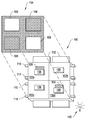
도 1a 는 예시적인 구현예에 따른, 디스플레이 장치의 일 예이다.
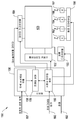
도 1b 는 예시적인 구현예에 따른, 도 1a 의 디스플레이 장치의 블록도이다.
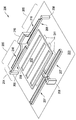
도 2 는 예시적인 구현예에 따른, 도 1a 의 MEMS-기반의 디스플레이에의 포함에 적당한 예시적인 셔터-기반의 광 변조기의 일 예이다.
도 3 은 예시적인 구현예에 따른, 도 1a 의 MEMS-기반의 디스플레이에 포함된 광 변조기들을 제어하는데 적당한 제어 매트릭스의 개략도이다.
도 4 는 예시적인 구현예에 따른, 도 3 의 제어 매트릭스에 접속된 셔터-기반의 광 변조기들의 어레이의 일 예이다.
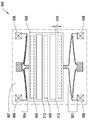
도 5a 는 예시적인 구현예에 따른, 제 1 듀얼-엑츄에이터 셔터-기반의 광 변조기의 일 예이다.
도 5b 는 예시적인 구현예에 따른, 제 2 듀얼-엑츄에이터 셔터-기반의 광 변조기의 일 예이다.
도 6 은 예시적인 구현예에 따른, 셔터-기반의 광 변조기들을 포함하는 디스플레이 장치의 단면도이다.
도 7a 는 예시적인 구현예에 따른, 셔터와 애퍼쳐 사이에 제 1 가능한 공간 관계를 가진 광 변조기의 일 예를 도시한다.
도 7b 는 예시적인 구현예에 따른, 셔터와 애퍼쳐 사이에 제 2 가능한 공간 관계를 가진 광 변조기의 일 예를 도시한다.
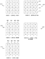
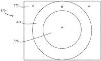
도 8a 내지 도 8c 는 디스플레이에서 픽셀 그룹핑 배열들의 예들을 도시한다.
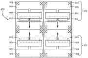
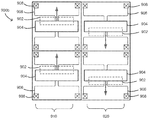
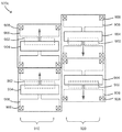
도 9a 내지 도 9c 는 어레이에서 광 변조기들의 2개의 그룹들의 특정의 배열들의 예들을 도시한다.
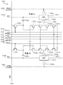
도 10 은 제어 매트릭스의 일 예이다.
도 11 은 대안적인 제어 매트릭스의 일 예이다.1A is an example of a display device according to an exemplary embodiment.
FIG. 1B is a block diagram of the display device of FIG. 1A, in accordance with an exemplary implementation.
FIG. 2 is an example of an exemplary shutter-based optical modulator suitable for inclusion in the MEMS-based display of FIG. 1A, according to an illustrative embodiment.
FIG. 3 is a schematic diagram of a control matrix suitable for controlling light modulators included in the MEMS-based display of FIG. 1A, in accordance with an exemplary implementation.
Figure 4 is an example of an array of shutter-based optical modulators connected to the control matrix of Figure 3, in accordance with an exemplary implementation.
5A is an example of a first dual-actuator shutter-based optical modulator, according to an exemplary implementation.
5B is an example of a second dual-actuator shutter-based optical modulator, according to an exemplary implementation.
6 is a cross-sectional view of a display device including shutter-based optical modulators, in accordance with an illustrative embodiment.
Figure 7A illustrates an example of an optical modulator having a first possible spatial relationship between a shutter and an aperture, in accordance with an exemplary embodiment.
7B shows an example of an optical modulator having a second possible spatial relationship between a shutter and an aperture, according to an exemplary embodiment.
Figures 8A-8C illustrate examples of pixel grouping arrangements in a display.
Figures 9A-9C illustrate examples of specific arrangements of two groups of optical modulators in an array.
10 is an example of a control matrix.
Figure 11 is an example of an alternative control matrix.
이미지들을 디스플레이하는 어떤 장치 및 방법들의 전반적인 이해를 제공하기 위해, 이제 어떤 예시적인 구현예들이 설명된다. 그러나, 본원에서 설명되는 시스템들 및 방법들이 거론되는 애플리케이션에 적합하게 적응되고 변경될 수도 있으며 본원에서 설명되는 시스템들 및 방법들이 다른 적당한 애플리케이션들에 채용될 수도 있으며, 이런 다른 부가들 및 변경들이 그 범위로부터 일탈하지 않을 것임을 당업자는 알 수 있을 것이다.In order to provide a general understanding of certain devices and methods for displaying images, some exemplary implementations are now described. However, it should be understood that the systems and methods described herein may be suitably adapted and modified for the applications discussed and that the systems and methods described herein may be employed in other appropriate applications, It will be apparent to those skilled in the art that the present invention will not depart from the scope.
본 개시물은 MEMS 셔터들과 같은 MEMS 광 변조기들의 어레이를 포함하는 MEMS-기반의 디스플레이에 관한 것이다. MEMS 광 변조기들은 대응하는 애퍼쳐들을 통과하는 광을 변조한다. MEMS 광 변조기들 중 많은 것들이 가청 주파수들의 시간 스케일들 특성을 넘어서 일제히 이동하게 되면, 이런 디스플레이는 바람직하지 않은 음향 잡음을 부산물로서 방출할 수도 있다. 부분적으로, 이런 잡음 방출들을 방지하기 위해, 본원에서 개시된 디스플레이들은 실질적으로 상이한 방향들로 광-방출 상태들로부터 광-차단 상태들로 작동하는 광 변조기들을 포함한다.The present disclosure relates to a MEMS-based display comprising an array of MEMS optical modulators, such as MEMS shutters. MEMS optical modulators modulate light passing through corresponding apertures. If many of the MEMS optical modulators move in unison over the time scales of the audible frequencies, such a display may also emit undesirable acoustic noise as a by-product. In part, to prevent such noise emissions, the displays disclosed herein include optical modulators that operate in light-interrupted states from light-emitting states in substantially different directions.
도 1a 는 예시적인 구현예에 따른, 디스플레이 장치 (100) 의 일 예이다. 디스플레이 장치 (100) 는 로우들 및 칼럼들에 배열된 복수의 광 변조기들 (102a-102d) (일반적으로, "광 변조기들 (102)") 을 포함한다. 디스플레이 장치 (100) 에서, 광 변조기들 (102a 및 102d) 은 광이 통과하도록 허용하는 개방된 상태에 있다. 광 변조기들 (102b 및 102c) 는 광의 통과를 차단하는 폐쇄된 상태에 있다. 광 변조기들 (102a-102d) 의 상태들을 선택적으로 설정함으로써, 디스플레이 장치 (100) 가 램프 또는 램프들 (105) 에 의해 조명되면, 백릿 (backlit) 디스플레이를 위한 이미지 (104) 를 형성하는데 이용될 수 있다.1A is an example of a display device 100, in accordance with an exemplary implementation. Display device 100 includes a plurality of
아래에 추가로 설명되는 다른 구현예에서, 장치는 장치의 정면으로부터 일어나는 주변 광의 반사에 의해 이미지를 형성할 수도 있다. 다른 구현예에서, 이 장치는 디스플레이의 정면에 위치된 램프 또는 램프들로부터의 광의 반사에 의해, 즉 정면 광의 사용에 의해 이미지를 형성할 수도 있다. 여전히 다른 구현예에서, 이 장치는 장치의 정면으로부터 생기는 주변 광과 백라이트로부터의 광 양자를 반사하는 반투과 모드에서 동작할 수도 있다. 일반적으로, 폐쇄된 또는 개방된 상태들 중 하나에서, 광 변조기들 (102) 은 예를 들어, 제한 없이, 광의 성질 또는 경로를 차단하거나, 반사하거나, 흡수하거나, 필터링하거나, 편광시키거나, 회절시키거나, 또는 아니면 변경함으로써, 광학적 경로에서의 광을 간섭한다.In another embodiment, described further below, the device may form an image by reflection of ambient light arising from the front of the device. In another embodiment, the apparatus may form an image by reflection of light from lamps or lamps located in front of the display, i. E. By use of front light. In still other embodiments, the apparatus may operate in a transflective mode that reflects both ambient light from the front of the device and light from the backlight. Generally, in one of the closed or open states, the optical modulators 102 may block, reflect, absorb, filter, polarize, or diffract the nature or path of light, for example, Or otherwise altering, the light in the optical path.
디스플레이 장치 (100) 에서, 각각의 광 변조기 (102) 는 이미지 (104) 에서의 픽셀 (106) 에 대응한다. 다른 구현예들에서, 디스플레이 장치 (100) 는 이미지 (104) 에 픽셀 (106) 을 형성하기 위해 복수의 광 변조기들을 이용할 수도 있다. 예를 들어, 디스플레이 장치 (100) 는 3개의 칼라-특정의 광 변조기들 (102) 을 포함할 수도 있다. 특정의 픽셀 (106) 에 대응하는 하나 이상의 칼라-특정의 광 변조기들 (102) 을 선택적으로 개방함으로써, 디스플레이 장치 (100) 는 이미지 (104) 에 칼라 픽셀 (106) 을 발생할 수도 있다. 다른 예에서, 디스플레이 장치 (100) 는 이미지 (104) 에 그레이스케일을 제공하기 위해 픽셀 (106) 당 2개 이상의 광 변조기들 (102) 을 포함한다. 이미지에 있어, "픽셀" 은 이미지의 해상도에 의해 정의되는 가장 작은 화소 (picture element) 에 대응한다. 디스플레이 장치 (100) 의 구조적 구성요소들에 있어, 용어 "픽셀" 은 이미지의 단일 픽셀을 형성하는 광을 변조하는데 이용되는, 결합된 기계적 및 전기적 구성요소들을 지칭한다.In the display device 100, each optical modulator 102 corresponds to a
디스플레이 장치 (100) 는 이미징 광학계를 필요로 하지 않는 직접-뷰 디스플레이이다. 사용자는 디스플레이 장치 (100) 를 직접 봄으로써 이미지를 본다. 대안적인 구현예들에서, 디스플레이 장치 (100) 는 투사형 디스플레이에 포함된다. 이런 구현예들에서, 디스플레이는 광을 스크린 상으로 또는 벽 상으로 투사함으로써, 이미지를 형성한다. 투사 애플리케이션들에서, 디스플레이 장치 (100) 는 투사된 이미지 (104) 보다 실질적으로 더 작다.Display device 100 is a direct-view display that does not require an imaging optics. The user sees the image by directly viewing the display device 100. In alternative embodiments, the display device 100 is included in a projection display. In these embodiments, the display forms an image by projecting light onto a screen or onto a wall. In the projection applications, the display device 100 is substantially smaller than the projected
직접-뷰 디스플레이들은 투과 또는 반사 모드로 동작할 수도 있다. 투과형 디스플레이에서, 광 변조기들은 디스플레이 뒤에 위치된 램프 또는 램프들로부터 일어나는 광을 필터링하거나 또는 선택적으로 차단한다. 램프들로부터의 광은 옵션적으로 광 가이드 또는 "백라이트" 에 주사된다. 투과형 직접-뷰 디스플레이 구현예들은, 광 변조기들을 포함하는 하나의 기판이 백라이트의 최상부 상에 바로 위치되는 샌드위치 어셈블리 배열을 용이하게 하기 위해, 플라스틱 또는 유리 기판들 상으로 장착된다. 일부 투과형 디스플레이 구현예들에서는, 백색 램프가 사용되며, 칼라 필터 재료를 각각의 변조기 (102) 와 결합함으로써, 칼라-특정의 광 변조기들이 제조된다. 다른 투과형 디스플레이 구현예들에서, 칼라들은 아래에 설명되는 바와 같이, 상이한 원색들을 가진 램프들의 교번하는 조명에 의해 필드 순차 칼라 방법 (field sequential color method) 을 이용하여 발생될 수 있다.Direct-view displays may operate in a transmissive or reflective mode. In transmissive displays, light modulators filter or selectively block light from lamps or lamps located behind the display. Light from the lamps is optionally scanned into a light guide or "backlight ". Transmissive direct-view display implementations are mounted on plastic or glass substrates to facilitate a sandwich assembly arrangement in which one substrate, including optical modulators, is placed directly on top of the backlight. In some transmissive display implementations, a white lamp is used, and color-specific optical modulators are fabricated by combining the color filter material with respective modulators 102. In other transmissive display implementations, the colors may be generated using a field sequential color method by alternating illumination of the lamps with different primary colors, as described below.
각각의 광 변조기 (102) 는 셔터 (108) 및 애퍼쳐 (109) 를 포함한다. 이미지 (104) 에서의 픽셀 (106) 을 조명하기 위해, 광이 뷰어 측으로 애퍼쳐 (109) 를 통과할 수 있도록 셔터 (108) 가 위치된다. 픽셀 (106) 을 점등하지 않은 채 유지하기 위해, 애퍼쳐 (109) 를 통한 광의 통과를 차단하도록 셔터 (108) 가 위치된다. 애퍼쳐 (109) 는 반사 또는 광-흡수 재료를 통해 패터닝된 개구에 의해 한정된다.Each optical modulator 102 includes a
반투과 구현예들에서, 각각의 광 변조기는 백라이트 (105) 로부터의 광 뿐만 아니라, 주변 광 양자를 변조한다. 하나의 특정의 구현예에서, 애퍼쳐들은, 애퍼쳐를 형성하기 위해 그렇지 않으면 에칭되는 반사 재료가 완전히 제거되지 않는다. 나머지 반사 재료는 이미지 (104) 의 부분을 형성하기 위해 입사광을 뷰어 측으로 되돌려 반사한다. 다른 구현예에서, 애퍼쳐들은 완전히 제거되며, 주변 광은 램프 (105) 뒤에 위치된 정면-대향 반사 층에 의해 반사된다.In semi-transparent embodiments, each optical modulator modulates both ambient light as well as light from
디스플레이의 반사 구현예들에서는, 백라이트 (105) 및 애퍼쳐들 (109) 을 포함하는 대신, 광 흡수 재료가 애퍼쳐들 (109) 대신 기판의 상부 표면에 도포되고, 광 반사 재료가 광 변조기들 (102) 의 상부 표면에 도포된다. 이의 대안으로, 광 반사 재료가 애퍼쳐 (109) 대신 기판의 상부 표면에 도포되고, 광 흡수 재료가 광 변조기들 (102) 의 상부 표면에 도포된다. 광 변조기들 (102a-102d) 의 상태들을 선택적으로 설정함으로써, 이미지 (104) 를 형성하기 위해 주변 또는 정면 광으로부터의 입사광이 선택적으로 반사되거나 또는 흡수될 수 있다.Instead of including the
디스플레이 장치는 또한 셔터들의 이동을 제어하기 위해 기판 및 광 변조기들에 접속된 제어 매트릭스를 포함한다. 제어 매트릭스는 픽셀들의 로우 당 적어도 하나의 기록-인에이블 상호접속부 (110) (또한, "스캐닝-라인 상호접속부" 로서 지칭됨), 픽셀들의 각각의 칼럼에 대해 하나의 데이터 상호접속부 (112), 및 모든 픽셀들에, 또는 디스플레이 장치 (100) 에서의 다수의 칼럼들 및 다수의 로우들 양자로부터의 적어도 픽셀들에 공통 전압을 제공하는 하나의 공통 상호접속부 (114) 를 포함한, 전기 상호접속부들의 시리즈 (예컨대, 상호접속부들 (110, 112, 및 114)) 를 포함한다. 적당한 전압 ("기록-인에이블링 전압 (Vwe)") 의 인가에 응답하여, 픽셀들의 주어진 로우에 대한 기록-인에이블 상호접속부 (110) 는 로우에서의 픽셀들에게 새로운 셔터 이동 명령들을 받아 들일 준비를 하게 한다. 데이터 상호접속부들 (112) 은 그 새로운 이동 명령들을 데이터 전압 펄스들의 형태로 통신한다. 데이터 상호접속부들 (112) 에 인가된 데이터 전압 펄스들은 일부 구현예들에서, 셔터들의 정전 이동에 직접적으로 기여한다. 다른 구현예들에서, 데이터 전압 펄스들은, 스위치들, 예컨대, 일반적으로 크기가 데이터 전압들보다 더 높은, 광 변조기들 (102) 에의 별개의 작동 전압들의 인가를 제어하는 트랜지스터들 또는 다른 비선형 회로 엘리먼트들을 제어한다. 이들 작동 전압들의 인가는 그러면 이후 셔터들 (108) 의 정전 구동 이동을 일으킨다.The display device also includes a control matrix connected to the substrate and the optical modulators for controlling the movement of the shutters. The control matrix includes at least one write-enable interconnect 110 (also referred to as a "scan-line interconnect") per row of pixels, one
도 1b 는 하나의 예시적인 구현예에 따른, 도 1a 의 디스플레이 장치 (100) 의 블록도 (150) 이다. 도 1a 및 도 1b 를 참조하면, 위에서 설명한 디스플레이 장치 (100) 의 엘리먼트들에 더해, 블록도 (150) 에 도시된 바와 같이, 디스플레이 장치 (100) 는 복수의 스캐닝 드라이버들 (152) (또한, "기록 인에이블링 전압 소스들" 로서 지칭됨) 및 복수의 데이터 드라이버들 (154) (또한, "데이터 전압 소스들" 로서 지칭됨) 을 포함한다. 스캐닝 드라이버들 (152) 은 기록 인에이블링 전압들을 스캐닝-라인 상호접속부들 (110) 에 인가한다. 데이터 드라이버들 (154) 은 데이터 전압들을 데이터 상호접속부들 (112) 에 인가한다. 디스플레이 장치의 일부 구현예들에서, 데이터 드라이버들 (154) 은 아날로그 데이터 전압들을 광 변조기들, 특히 이미지 (104) 의 그레이 스케일이 아날로그 방식으로 도출되는 광 변조기들에 제공하도록 구성된다. 아날로그 동작 시, 광 변조기들 (102) 은, 중간 전압들의 범위가 데이터 상호접속부들 (112) 을 통해서 인가될 때 셔터들 (108) 에서 중간 개방된 상태들의 범위, 따라서, 이미지 (104) 에서 중간 조명 상태들 또는 그레이 스케일들의 범위를 초래하도록, 설계된다.FIG. 1B is a block diagram 150 of the display device 100 of FIG. 1A according to one exemplary embodiment. 1A and 1B, in addition to the elements of the display device 100 described above, the display device 100 includes a plurality of scanning drivers 152 (also referred to as " Write enable voltage sources ") and a plurality of data drivers 154 (also referred to as" data voltage sources "). The scanning
다른 경우들에서, 데이터 드라이버들 (154) 은 단지 2, 3, 또는 4 디지털 전압 레벨들의 감소된 세트를 제어 매트릭스에 인가하도록 구성된다. 이들 전압 레벨들은 디지털 방식으로, 셔터들 (108) 의 각각에 대해 개방된 상태 또는 폐쇄된 상태를 설정하도록 설계된다.In other cases, the
스캐닝 드라이버들 (152) 및 데이터 드라이버들 (154) 은 디지털 제어기 회로 (156) (또한, "제어기 (156)" 로서 지칭됨) 에 접속된다. 제어기 (156) 는 입력 프로세싱 모듈 (158) 을 포함하며, 이 입력 프로세싱 모듈은 인입하는 이미지 신호 (157) 를 디스플레이 (100) 의 공간 어드레싱 및 그레이 스케일 능력들에 적당한 디지털 이미지 포맷으로 프로세싱한다. 각각의 이미지의 픽셀 로케이션 및 그레이 스케일 데이터는 데이터 드라이버들 (154) 에 요구될 때 데이터가 공급될 수 있도록 프레임 버퍼 (159) 내에 저장된다. 데이터는 로우들로 그리고 이미지 프레임들로 그룹화된 미리 결정된 시퀀스들로 편성되는 대개 직렬 방식 (serial fashion) 으로, 데이터 드라이버들 (154) 로 전송된다. 데이터 드라이버들 (154) 은 직렬 대 병렬 데이터 변환기들, 레벨 시프팅, 및 일부 애플리케이션들의 경우, 디지털 대 아날로그 전압 변환기들을 포함할 수 있다.The scanning
디스플레이 (100) 장치는 옵션적으로, 공통 전압 소스들로서 또한 지칭되는 공통 드라이버들 (153) 의 세트를 포함한다. 일부 구현예들에서, 공통 드라이버들 (153) 은 예를 들어, 전압을 공통 상호접속부들 (114) 의 시리즈에 공급함으로써, DC 공통 퍼텐셜을 광 변조기들 (103) 의 어레이 내의 모든 광 변조기들에 제공한다. 다른 구현예들에서, 공통 드라이버들 (153) 은, 제어기 (156) 로부터의 지령들에 뒤이어서, 전압 펄스들 또는 신호들을, 예를 들어, 어레이 (103) 의 다수의 로우들 및 칼럼들에서의 모든 광 변조기들의 동시적인 구동을 행하거나 및/또는 개시할 수 있는 글로벌 구동 펄스들을, 광 변조기들 (103) 의 어레이로 발한다.The display 100 device optionally includes a set of
상이한 디스플레이 기능들을 위한 드라이버들 모두 (예컨대, 스캐닝 드라이버들 (152), 데이터 드라이버들 (154), 및 공통 드라이버들 (153)) 는 제어기 (156) 에서의 타이밍-제어 모듈 (160) 에 의해 시간-동기화된다. 모듈 (160) 로부터의 타이밍 지령들은, 램프 드라이버들 (168) 을 통한 적색, 녹색 및 청색 및 백색 램프들 (각각, 162, 164, 166, 및 167) 의 조명, 픽셀들 (103) 의 어레이 내 특정의 로우들의 기록-인에이블링 및 시퀀싱, 데이터 드라이버들 (154) 로부터의 전압들의 출력, 및 광 변조기 작동을 위해 공급하는 전압들의 출력을 조정한다.All of the drivers (e.g., scanning
제어기 (156) 는 어레이 (103) 에서의 셔터들 (108) 각각이 새로운 이미지 (104) 에 적당한 조명 레벨들로 재설정될 수 있는 시퀀싱 또는 어드레싱 방식을 결정한다. 적당한 어드레싱, 이미지 형성, 및 그레이 스케일 기법들의 세부 사항들은 본원에 참조로 포함된 미국 특허출원 번호 제 11/326,696호 및 제 11/643,042호에서 발견될 수 있다. 새로운 이미지들 (104) 은 주기적인 간격들로 설정될 수도 있다. 예를 들어, 비디오 디스플레이들에 있어, 비디오의 칼라 이미지들 (104) 또는 프레임들은 10 내지 300 Hertz 의 범위에 걸친 주파수들에서 리프레시된다. 일부 구현예들에서, 어레이 (103) 에 대한 이미지 프레임의 설정은, 교번하는 이미지 프레임들이 적색, 녹색, 및 청색과 같은 칼라들의 교번하는 시리즈로 조명되도록, 램프들 (162, 164, 및 166) 의 조명과 동기화된다. 각각의 개개의 칼라에 대한 이미지 프레임들은 칼라 서브-프레임으로서 지칭된다. 필드 순차 칼라 방법으로서 지칭되는 이 방법에서는, 칼라 서브-프레임들이 20 Hz 를 초과하는 주파수들로 교번되면, 인간 두뇌는 교번하는 프레임 이미지들을 넓고 연속적인 범위의 칼라를 갖는 이미지의 지각으로 평균할 것이다. 대안적인 구현예들에서, 원색들을 가진 4개 또는 이상의 램프들이 적색, 녹색, 및 청색 이외에 원색들을 채용하는 디스플레이 장치 (100) 에 채용될 수 있다.The
일부 구현예들에서, 디스플레이 장치 (100) 가 개방된 상태와 폐쇄된 상태 사이의 셔터들 (108) 의 디지털 스위칭용으로 설계되는 경우, 제어기 (156) 는 적당한 그레이 스케일을 가진 이미지들 (104) 을 발생하기 위해 이미지 프레임들 사이의 어드레싱 시퀀스 및/또는 시간 간격들을 결정한다. 특정의 프레임에서 셔터 (108) 가 개방되는 시간의 양을 제어함으로써 그레이스케일의 가변 레벨들을 발생하는 프로세스는 시분할 그레이 스케일로서 지칭된다. 시분할 그레이 스케일의 일 구현예에서, 제어기 (156) 는 그 픽셀에 대해 소망되는 조명 레벨 또는 그레이 스케일에 따라서, 셔터 (108) 가 개방된 상태로 유지하도록 허용되는 각각의 프레임 내 시간 기간 또는 시간의 작은 부분을 결정한다. 다른 구현예들에서, 각각의 이미지 프레임에 대해, 제어기 (156) 는 어레이 (103) 의 다수의 로우들 및 칼럼들에서 복수의 서브-프레임 이미지들을 설정하고, 제어기는 각각의 서브-프레임 이미지가 그레이 스케일에 대해 코딩된 단어 내에 채용된 그레이 스케일 값 또는 유의도 값에 비례하여 조명되는 지속기간을 변경한다. 예를 들어, 서브-프레임 이미지들의 시리즈에 대한 조명 시간들은 2진 코딩 급수 (series) 1,2,4,8.. 에 비례하여 변화될 수도 있다. 어레이 (103) 에서의 각각의 픽셀에 대한 셔터들 (108) 은 그후 그레이 레벨에 대한 픽셀의 2진 코딩된 단어 내의 대응하는 위치에서의 값에 따라서 서브-프레임 이미지 내에서 개방된 또는 폐쇄된 상태로 설정된다.In some implementations, when the display device 100 is designed for digital switching of the
다른 구현예들에서, 제어기는 램프들 (162, 164, 및 166) 로부터의 광의 강도를 특정의 서브-프레임 이미지에 대해 원하는 그레이 스케일 값에 비례하여 변경한다. 다수의 하이브리드 기법들이 또한 셔터들 (108) 의 어레이로부터 칼라들 및 그레이 스케일을 형성하는데 이용될 수도 있다. 예를 들어, 위에서 설명한 시분할 기법들이 픽셀 당 다수의 셔터들 (108) 의 사용과 결합될 수 있거나, 또는 특정의 서브-프레임 이미지에 대한 그레이 스케일 값이 서브-프레임 타이밍과 램프 강도 양자의 조합을 통해서 확립될 수 있다. 이들 및 다른 구현예들의 세부 사항들은 위에서 참조한 미국 특허출원 제 11/643,042호에서 발견될 수 있다.In other implementations, the controller changes the intensity of the light from the
일부 구현예들에서, 이미지 상태 (104) 에 대한 데이터가 제어기 (156) 에 의해 변조기 어레이 (103) 로, 스캐닝 라인들로서 또한 지칭되는 개개의 로우들의 순차적인 어드레싱에 의해, 로드된다. 시퀀스에서 각각의 로우 또는 스캐닝 라인에 대해, 스캐닝 드라이버 (152) 는 기록-인에이블 전압을 그 어레이 (103) 의 로우에 대한 기록 인에이블 상호접속부 (110) 에 인가하고, 후속하여 데이터 드라이버 (154) 는 선택된 로우에서의 각각의 칼럼에 대해, 원하는 셔터 상태들에 대응하는 데이터 전압들을 공급한다. 이 프로세스는 그 어레이에서의 모든 로우들에 대해 데이터가 로드될 때까지 반복한다. 일부 구현예들에서, 데이터 로딩을 위한 선택된 로우들의 시퀀스는 선형이며, 어레이에서 최상부로부터 최저부로 진행한다. 다른 구현예들에서, 선택된 로우들의 시퀀스는 시각적 아티팩트들을 최소화하기 위해 의사-무작위로 추출된다. 그리고, 다른 구현예들에서, 시퀀싱은 블록들로 편성되며, 여기서, 블록에 있어, 이미지 상태 (104) 의 단지 어떤 작은 부분에 대한 데이터가 예를 들어, 어레이의 단지 매 5번째 로우를 차례로 어드레싱함으로써, 어레이로 로드된다.In some implementations, data for the
일부 구현예들에서, 이미지 데이터를 어레이 (103) 에 로드하는 프로세스는 셔터들 (108) 을 작동하는 프로세스와 시간적으로 분리된다. 이들 구현예들에서, 변조기 어레이 (103) 는 어레이 (103) 에서의 각각의 픽셀에 대한 데이터 메모리 엘리먼트들을 포함할 수도 있으며, 제어 매트릭스는 메모리 엘리먼트들에 저장된 데이터에 따라서 셔터들 (108) 의 동시적인 작동을 개시하기 위해 공통 드라이버 (153) 로부터 트리거 신호들을 반송하는 글로벌 작동 상호접속부를 포함할 수도 있다. 여러 어드레싱 시퀀스들은, 이들 중 많은 것들이 미국 특허출원 제 11/643,042호에 설명되어 있는데, 타이밍 제어 모듈 (160) 에 의해 조정될 수 있다.In some implementations, the process of loading the image data into the
대안적인 구현예들에서, 픽셀들을 제어하는 제어 매트릭스 및 픽셀들 (103) 의 어레이는 직사각형의 로우들 및 칼럼들 이외의 구성들로 배열될 수도 있다. 예를 들어, 픽셀들은 6각형의 어레이들 또는 곡선형의 로우들 및 칼럼들로 배열될 수 있다. 일반적으로, 본원에서 사용할 때, 용어 스캐닝-라인은 기록-인에이블링 상호접속부를 공유하는 임의의 복수의 픽셀들을 지칭할 것이다.In alternative embodiments, the control matrix that controls the pixels and the array of
일부 구현예들에서, 변조기들의 어레이는 그들의 각각의 애퍼쳐들에 대해 상이한 공간 방위들 (spatial orientations) 을 가진 2개 이상 그룹들로 분할될 수도 있다. 입력 프로세싱 모듈 (158) 은 각각의 변조기를 광-차단 상태로부터 광-투과 상태로 작동하는 모션의 방향을 결정하기 위해서, 각각의 픽셀의 공간 방위의 맵 및 프로세스 제어 신호들을 제어 매트릭스로 전송하기 전에 추가적으로 저장할 수도 있다.In some implementations, the arrays of modulators may be divided into two or more groups with different spatial orientations for their respective apertures. The
디스플레이 (100) 는 타이밍 제어 모듈 (160), 프레임 버퍼 (159), 스캐닝 드라이버들 (152), 데이터 드라이버들 (154), 및 드라이버들 (153 및 168) 을 포함한 복수의 기능 블록들을 포함한다. 각각의 블록은 식별가능한 하드웨어 회로 및/또는 실행가능한 코드의 모듈을 나타내는 것으로 해석될 수도 있다. 일부 구현예들에서, 기능 블록들은 회로 보드들 및/또는 케이블들에 의해 함께 접속된 별개의 칩들 또는 회로들로서 제공된다. 대안적으로, 이들 회로들의 많은 회로들은 유리 또는 플라스틱의 동일한 기판 상에 픽셀 어레이 (103) 와 함께 제조될 수도 있다. 다른 구현예들에서, 블록도 (150) 로부터의 다수의 회로들, 드라이버들, 프로세서들, 및/또는 제어 기능들은 단일 실리콘 칩 내에 함께 통합되고, 그후 픽셀 어레이 (103) 를 유지하는 투명한 기판에 직접 본딩될 수도 있다.The display 100 includes a plurality of functional blocks including a
제어기 (156) 는 제어기 (156) 내에서 구현되는 어드레싱, 칼라, 및/또는 그레이 스케일 알고리즘들이 특정의 애플리케이션들의 요구들에 따라서 변경될 수 있는 프로그래밍 링크 (180) 를 포함한다. 일부 구현예들에서, 프로그래밍 링크 (180) 는 주변 광 또는 온도 센서들과 같은 환경 센서들로부터 정보를 전달하며, 그 결과, 제어기 (156) 가 환경 조건들에 대응하여 이미징 모드들 또는 백라이트 전력을 조정할 수 있다. 제어기 (156) 는 또한 광 변조기 작동 뿐만 아니라 램프들에 요구되는 전력을 제공하는 전원 입력 (182) 을 포함한다. 드라이버들 (152 153, 154, 및/또는 168) 은 또한 182 에서의 입력 전압을 셔터들 (108) 의 작동 또는 램프들 (162, 164, 166, 및 167) 과 같은 램프들의 조명에 충분한 여러 전압들로 변환하는 DC-DC 변환기들을 포함하거나 또는 결합될 수도 있다.
도 2 는 예시적인 구현예에 따른, 도 1a 의 MEMS-기반의 디스플레이 장치 (100) 에의 포함에 적당한 예시적인 셔터-기반의 광 변조기 (200) 의 사시도이다. 셔터-기반의 광 변조기 (200) (또한, 셔터 어셈블리 (200) 로서 지칭됨) 는 엑츄에이터 (204) 에 커플링된 셔터 (202) 를 포함한다. 엑츄에이터 (204) 는 미국특허 번호 제 7,271,945호에 설명된 바와 같이, 2개의 별개의 순응 전극 빔 엑츄에이터들 (205; compliant electrode beam actuators) ("엑츄에이터들 (205)") 로부터 형성된다. 셔터 (202) 는 일 측면 상에서 엑츄에이터들 (205) 에 커플링한다. 엑츄에이터들 (205) 은 셔터 (202) 를 표면 (203) 에 평행한 모션 평면에서 표면 (203) 위를 가로질러 이동시킨다. 셔터 (202) 의 반대 측면은 엑츄에이터 (204) 에 의해 작용되는 힘들에 반대로 작용하는 복원력을 제공하는 스프링 (207) 에 커플링한다.FIG. 2 is a perspective view of an exemplary shutter-based
각각의 엑츄에이터 (205) 는 셔터 (202) 를 로드 앵커 (208; load anchor) 에 접속하는 순응 로드 빔 (206; compliant load beam) 을 포함한다. 순응 로드 빔들 (206) 과 함께 로드 앵커들 (208) 은 셔터 (202) 를 표면 (203) 에 가장 가깝게 현수하여 유지하는 기계적 지지체들로서 기능한다. 로드 앵커들 (208) 은 순응 로드 빔들 (206) 및 셔터 (202) 를 표면 (203) 에 물리적으로 접속하고 로드 빔들 (206) 을 바이어스 전압에, 일부 경우, 접지에 전기적으로 접속한다. 각각의 엑츄에이터 (205) 은 또한 각각의 로드 빔 (206) 에 인접하게 위치된 순응 구동 빔 (216; compliant drive beam) 을 포함한다. 구동 빔들 (216) 은 일 단부에서 구동 빔들 (216) 사이에 공유된 구동 빔 앵커 (218) 에 커플링한다. 각각의 구동 빔 (216) 의 타 단부는 자유롭게 이동한다. 각각의 구동 빔 (216) 은 구동 빔 (216) 의 자유 단 및 로드 빔 (206) 의 앵커된 단부에 가까이 로드 빔 (206) 에 가장 가깝도록 만곡된다.Each
표면 (203) 은 광의 통과를 가능하게 하는 하나 이상의 애퍼쳐들 (211) 을 포함한다. 셔터 어셈블리 (200) 가 예를 들어, 실리콘으로 제조된 불투명 기판 상에 형성되면, 표면 (203) 은 기판의 표면이고, 기판을 통해서 홀들의 어레이를 에칭함으로써 애퍼쳐들 (211) 이 형성된다. 셔터 어셈블리 (200) 가 예를 들어, 유리 또는 플라스틱으로 제조된 투명 기판 상에 형성되면, 표면 (203) 은 기판 상에 퇴적된 광 차단 층의 표면이고, 표면 (203) 을 홀들 (211) 의 어레이로 에칭함으로써 애퍼쳐들이 형성된다. 애퍼쳐들 (211) 은 일반적으로 형태가 원형, 타원형, 다각형, S자형 (serpentine), 또는 불규칙적일 수 있다.
동작 시, 광 변조기 (200) 를 포함하는 디스플레이 장치는 구동 빔 앵커 (218) 를 통해서 전기 퍼텐셜을 구동 빔들 (216) 에 인가한다. 제 2 전기 퍼텐셜이 로드 빔들 (206) 에 인가될 수도 있다. 구동 빔들 (216) 과 로드 빔들 (206) 사이의 최종 퍼텐셜 차이가 구동 빔들 (216) 의 자유 단들을 로드 빔들 (206) 의 앵커된 단부들 측으로 당기고, 로드 빔들 (206) 의 셔터 단부들을 구동 빔들 (216) 의 앵커된 단부들 측으로 당김으로써, 셔터 (202) 를 구동 앵커 (218) 측으로 가로질러 구동한다. 순응 부재들 (206) 은 스프링들로서 작용하며, 그 결과, 빔들 (206 및 216) 을 가로지르는 전압이 제거될 때, 로드 빔들 (206) 이 셔터 (202) 를 그의 초기 위치로 되밀어, 로드 빔들 (206) 에 저장된 스트레스를 해제한다.In operation, the display device including the
탄성 셔터 어셈블리로서 또한 지칭되는 셔터 어셈블리 (200) 는, 전압들이 제거된 후 셔터를 그의 휴지 또는 이완된 위치로 복귀시키기 위해, 스프링과 같은 수동적인 복원력을 포함한다. 다수의 탄성 복원 메카니즘들 및 여러 정전 커플링들은, 단지 일 예인 셔터 어셈블리 (200) 에 도시된 순응 빔들로 또는 정전 엑츄에이터들과 함께, 설계될 수 있다. 다른 예들은 본원에 참조로 포함된, 미국 특허 제 7,271,945호 및 미국 특허출원 번호 제 11/326,696호에 설명되어 있다. 예를 들어, 동작의 "개방된" 대 "폐쇄된" 상태들 사이의 갑작스러운 전이를 조력하고, 그리고 많은 경우, 셔터 어셈블리에 쌍-안정하거나 또는 히스테리시스 동작 특성을 제공하는, 높은 비선형 전압-변위 응답이 제공될 수 있다. 다른 정전 엑츄에이터들은 예를 들어, 아날로그 그레이 스케일 동작에서, 더 증분된 전압-변위 응답들로 그리고 상당히 감소된 히스테리시스로 설계될 수 있다.The
탄성 셔터 어셈블리 내의 엑츄에이터 (205) 가 폐쇄된 또는 작동된 위치와 이완된 위치 사이에 동작한다고 한다. 설계자는, 그러나, 엑츄에이터 (205) 가 그의 이완된 위치에 있을 때는 언제나, 셔터 어셈블리 (200) 가 "개방된" 상태, 즉 광을 통과시키는 상태에 있거나, 또는 "폐쇄된" 상태, 즉 광을 차단하는 상태에 있게, 애퍼쳐들 (211) 을 배치하도록 선택할 수도 있다.It is assumed that the
일부 구현예들에서, 셔터 어셈블리는 제어 전자기기가 셔터들을 개방된 상태 및 폐쇄된 상태 각각으로 정전 구동할 수 있도록, "개방된" 및 "폐쇄된" 엑츄에이터들의 듀얼 세트를 포함한다.In some embodiments, the shutter assembly includes a dual set of "open" and "closed" actuators such that the control electronics can electrostatically drive the shutters into the open and closed states, respectively.
미국 특허 제 7,271,945호 및 미국 특허출원 번호 제 11/326,696호는 셔터들의 어레이가 이미지들을, 많은 경우, 동화상들을, 적당한 그레이 스케일로 발생하기 위해 제어 매트릭스를 통해서 제어될 수도 있는 다양한 방법들을 설명하고 있다. 일부의 경우, 제어는 디스플레이의 주변부 상의 드라이버 회로들에 접속된 로우 및 칼럼 상호접속부들의 수동 매트릭스 어레이에 의해 달성된다. 다른 경우, 디스플레이의 속도, 그레이 스케일 및/또는 전력 소산 성능을 향상시키기 위해 어레이의 각각의 픽셀 (소위 활성 매트릭스) 내에 스위칭 및/또는 데이터 저장 엘리먼트들을 포함하는 것이 적절하다.U.S. Patent No. 7,271,945 and U.S. Patent Application Serial No. 11 / 326,696 describe various methods by which an array of shutters may be controlled through a control matrix to generate images, often moving images, in the appropriate grayscale . In some cases, control is accomplished by a passive matrix array of row and column interconnects connected to driver circuits on the periphery of the display. In other cases, it is appropriate to include switching and / or data storage elements within each pixel (so-called active matrix) of the array to improve the speed, gray scale and / or power dissipation performance of the display.
도 3 은 예시적인 구현예에 따른, 도 1a 의 MEMS-기반의 디스플레이 장치 (100) 에 포함된 광 변조기들을 제어하는데 적합한 제어 매트릭스 (300) 의 개략도이다. 도 4 는 예시적인 구현예에 따른, 도 3 의 제어 매트릭스 (300) 에 접속된 셔터-기반의 광 변조기들의 어레이 (320) 의 일 예이다. 제어 매트릭스 (300) 는 픽셀들 (320) 의 어레이 ("어레이 (320)") 를 어드레스할 수도 있다. 각각의 픽셀 (301) 은 엑츄에이터 (303) 에 의해 제어되는, 도 2 의 셔터 어셈블리 (200) 와 같은 탄성 셔터 어셈블리 (302) 를 포함한다. 각각의 픽셀은 또한 애퍼쳐들 (324) 을 포함하는 애퍼쳐 층 (322) 을 포함한다. 셔터 어셈블리 (302) 및 이의 변형들과 같은, 추가적인 셔터 어셈블리들의 전기적 및 기계적 설명들은, 미국 특허 제 7,271,945호 및 미국 특허출원 번호 제 11/326,696호에서 발견될 수 있다. 대안적인 제어 매트릭스들의 설명들은 또한 도 10 및 도 11 과 관련하여 아래에서, 뿐만 아니라 미국 특허출원 번호 제 11/607,715호에서 발견될 수 있다.FIG. 3 is a schematic diagram of a
제어 매트릭스 (300) 는 셔터 어셈블리들 (302) 이 형성된 기판 (304) 의 표면 상의 확산된 또는 박막-퇴적된 전기 회로로서 제조된다. 제어 매트릭스 (300) 는 제어 매트릭스 (300) 에서의 픽셀들 (301) 의 각각의 로우에 대한 스캐닝-라인 상호접속부 (306), 및 제어 매트릭스 (300) 에서의 픽셀들 (301) 의 각각의 칼럼에 대한 데이터-상호접속부 (308) 를 포함한다. 각각의 스캐닝-라인 상호접속부 (306) 는 기록-인에이블링 전압 소스 (307) 를 픽셀들 (301) 의 대응하는 로우에서 픽셀들 (301) 에 전기적으로 접속한다. 각각의 데이터 상호접속부 (308) 는 데이터 전압 소스 ("Vd 소스") (309) 를 픽셀들 (301) 의 대응하는 칼럼에서 픽셀들 (301) 에 전기적으로 접속한다. 제어 매트릭스 (300) 에서, 데이터 전압 (Vd) 은 셔터 어셈블리들 (302) 에 대부분의 작동 에너지를 제공한다. 따라서, 데이터 전압 소스 (309) 는 또한 작동 전압 소스로서 기능한다.The
도 3 및 도 4 를 참조하면, 픽셀들 (320) 의 어레이에서 각각의 픽셀 (301) 에 대해 또는 각각의 셔터 어셈블리 (302) 에 대해, 제어 매트릭스 (300) 는 트랜지스터 (310) 및 커패시터 (312) 를 포함한다. 각각의 트랜지스터 (310) 의 게이트는 픽셀 (301) 이 위치된 어레이 (320) 에서 로우의 스캐닝-라인 상호접속부 (306) 에 전기적으로 접속된다. 각각의 트랜지스터 (310) 의 소스는 그의 대응하는 데이터 상호접속부 (308) 에 전기적으로 접속된다. 각각의 셔터 어셈블리 (302) 의 엑츄에이터들 (303) 은 2개의 전극들을 포함한다. 각각의 트랜지스터 (310) 의 드레인은 대응하는 커패시터 (312) 의 하나의 전극에, 그리고 대응하는 엑츄에이터 (303) 의 전극들 중 하나에 병렬로 전기적으로 접속된다. 셔터 어셈블리 (302) 에서 커패시터 (312) 의 다른 전극 및 엑츄에이터 (303) 의 다른 전극은 공통 또는 접지 퍼텐셜에 접속된다. 대안적인 구현예들에서, 트랜지스터들 (310) 은 반도체 다이오드들 및 또는 금속-절연체-금속 샌드위치 유형 스위칭 소자들로 대체될 수 있다.3 and 4, for each
동작 시, 이미지를 형성하기 위해, 제어 매트릭스 (300) 는 Vwe 을 각각의 스캐닝-라인 상호접속부 (306) 에 차례로 인가함으로써, 어레이 (320) 에서 각각의 로우를 시퀀스로 기록-인에이블한다. 기록-인에이블된 로우에 대해, 로우에서 픽셀들 (301) 의 트랜지스터들 (310) 의 게이트들로의 Vwe 의 인가는, 퍼텐셜을 셔터 어셈블리 (302) 의 엑츄에이터 (303) 에 인가하기 위해, 데이터 상호접속부들 (308) 을 통해서 트랜지스터들 (310) 을 통한 전류의 흐름을 가능하게 한다. 로우가 기록-인에이블되는 동안, 데이터 전압들 (Vd) 이 데이터 상호접속부들 (308) 에 선택적으로 인가된다. 아날로그 그레이 스케일을 제공하는 구현예들에서, 각각의 데이터 상호접속부 (308) 에 인가되는 데이터 전압은 기록-인에이블된 스캐닝-라인 상호접속부 (306) 와 데이터 상호접속부 (308) 의 교차점에 위치된 픽셀 (301) 의 원하는 휘도와 관련하여 변화된다. 디지털 제어 방식들을 제공하는 구현예들에서, 데이터 전압은 상대적으로 낮은 크기 전압 (즉, 접지 근처의 전압) 으로, 또는 Vat (작동 임계 전압) 을 만족하거나 초과하도록 선택된다. 데이터 상호접속부 (308) 에의 Vat 의 인가에 응답하여, 대응하는 셔터 어셈블리 (302) 에서의 엑츄에이터 (303) 가 작동하여, 그 셔터 어셈블리 (302) 에서 셔터를 개방한다. 데이터 상호접속부 (308) 에 인가되는 전압은, 심지어 제어 매트릭스 (300) 가 Vwe 를 로우에 인가하는 것을 중지한 후에도, 픽셀 (301) 의 커패시터 (312) 에 저장된 채 유지한다. 따라서, 셔터 어셈블리 (302) 를 작동하는데 충분히 긴 시간 동안 로우 상의 전압 Vwe 을 대기하고 유지하는 것이 요구되지 않는다; 이런 작동은 기록-인에이블링 전압이 로우로부터 제거된 후에 진행할 수 있다. 커패시터들 (312) 은 또한 이미지 프레임의 조명에 필요로 하는 기간들 동안 작동 명령들을 저장하는, 어레이 (320) 내 메모리 엘리먼트들로서 기능한다.In operation, to form the image, the
어레이 (320) 의 제어 매트릭스 (300) 뿐만 아니라 픽셀들 (301) 이 기판 (304) 상에 형성된다. 어레이는 어레이 (320) 에서 각각의 픽셀들 (301) 에 대한 애퍼쳐들 (324) 의 세트를 포함하는, 기판 (304) 상에 배치된 애퍼쳐 층 (322) 을 포함한다. 애퍼쳐들 (324) 은 각각의 픽셀에서 셔터 어셈블리들 (302) 과 정렬된다. 일 구현예에서, 기판 (304) 은 투명한 재료, 예컨대 유리 또는 플라스틱으로 제조된다. 다른 구현예에서, 기판 (304) 은 불투명 재료로 제조되지만, 홀들이 에칭되어 애퍼쳐들 (324) 을 형성한다.
셔터 어셈블리들 (302) 의 구성요소들은 제어 매트릭스 (300) 와 동시에 또는 동일한 기판 상의 후속 프로세싱 단계들에서 프로세싱된다. 제어 매트릭스 (300) 에서 전기적 구성요소들은 액정 디스플레이들용 박막 트랜지스터 어레이들의 제조와 공통적인 많은 박막 기법들을 이용하여 제조된다. 가용 기법들은 본원에 참조로 포함된, Den Boer, Active Matrix Liquid Crystal Displays (Elsevier, Amsterdam, 2005) 에 설명되어 있다. 셔터 어셈블리들은 미세 기계가공의 기술과 유사한 기법들을 이용하여 또는 마이크로메카니컬 (즉, MEMS) 디바이스들의 제조로부터 제조된다. 많은 적용가능한 박막 MEMS 기법들은, 본원에 참조로 포함된, Rai-Choudhury, ed., Handbook of Microlithography, Micromachining & Microfabrication (SPIE Optical Engineering Press, Bellingham, Wash. 1997) 에 설명되어 있다. 유리 기판들 상에 형성된 MEMS 광 변조기들에 고유한 제조 기법들은 본원에 참조로 포함된, 미국 특허 제 7,405,852호 및 제 7,675,665호에서 발견될 수 있다. 예를 들어, 그들 애플리케이션들에서 설명하는 바와 같이, 셔터 어셈블리 (302) 는 화학 기상 증착 프로세스에 의해 퇴적되는 비결정 실리콘의 박막들로부터 형성될 수 있다.The components of the
셔터 어셈블리 (302) 는 엑츄에이터 (303) 와 함께 쌍-안정될 수 있다. 즉, 셔터들은 적어도 2개의 평형 위치들 (예컨대, 개방된 또는 폐쇄된) 에, 그들을 어느 하나의 위치에 유지하는데 거의 또는 전혀 전력이 요구되지 않고, 존재할 수 있다. 좀더 자세하게 설명하면, 셔터 어셈블리 (302) 는 기계적으로 쌍-안정일 수 있다. 일단 셔터 어셈블리 (302) 의 셔터가 적소에 배치되면, 어떤 전기적 에너지 또는 유지 전압도 그 위치를 유지하는데 요구되지 않는다. 셔터 어셈블리 (302) 의 물리적인 엘리먼트들 상의 기계적 스트레스들은 셔터를 적소에 유지할 수 있다.The
셔터 어셈블리 (302) 는 엑츄에이터 (303) 와 함께 또한 전기적으로 쌍-안정될 수 있다. 전기적으로 쌍-안정한 셔터 어셈블리에서, (셔터가 개방되거나 또는 폐쇄된 채) 폐쇄된 엑츄에이터에 인가되면, 반대작용력이 셔터 상에 가해지더라도, 엑츄에이터를 폐쇄된 상태로 그리고 셔터를 적소에 유지하는, 셔터 어셈블리의 작동 전압 아래의 전압들의 범위가 존재한다. 반대작용력은 셔터-기반의 광 변조기 (200) 에서 스프링 (207) 과 같은 스프링에 의해 가해질 수도 있거나, 또는 반대작용력은 "개방된" 또는 "폐쇄된" 엑츄에이터와 같은 반대작용 엑츄에이터에 의해 가해질 수도 있다.The
광 변조기 어레이 (320) 는 픽셀 당 단일 MEMS 광 변조기를 갖는 것으로 도시된다. 다수의 MEMS 광 변조기들이 각각의 픽셀에 제공되어 각각의 픽셀에서 단지 2진 "온" 또는 "오프" 광학적 상태들 이상의 가능성을 제공하는 다른 구현예들이 가능하다. 픽셀에 다수의 MEMS 광 변조기들이 제공되고 그리고 광 변조기들의 각각과 결합되는 애퍼쳐들 (324) 이 동등하지 않은 영역들을 갖는, 어떤 유형들의 코딩된 영역 분할 그레이 스케일이 가능하다.The
도 5a 및 도 5b 는 예시적인 구현예에 따른, 듀얼 엑츄에이터 셔터-기반의 광 변조기들 (500) 의 예들을 도시한다. 광 변조기 (500) 는 도 5a 에 개방된 상태로 도시된다. 도 5b 는 폐쇄된 상태에서의 듀얼 엑츄에이터 셔터 어셈블리 (500) 의 도면이다. 셔터 어셈블리 (500) 는 셔터 (506) 의 양 측면 상의 엑츄에이터들 (502 및 504) 을 포함한다. 각각의 엑츄에이터 (502 및 504) 는 독립적으로 제어된다. 제 1 엑츄에이터, 즉, 셔터-개방 엑츄에이터 (502) 는 셔터 (506) 를 개방하도록 기능한다. 제 2 반대작용 엑츄에이터, 즉, 셔터-폐쇄 엑츄에이터 (504) 는 셔터 (506) 를 폐쇄하도록 기능한다. 엑츄에이터들 (502 및 504) 양자는 순응 빔 전극 엑츄에이터들이다. 엑츄에이터들 (502 및 504) 은 셔터가 위에 걸쳐서 현수되는 애퍼쳐 층 (507) 에 평행한 평면에서 셔터 (506) 를 구동함으로써 셔터 (506) 를 개방하고 폐쇄한다. 셔터 (506) 는 엑츄에이터들 (502 및 504) 에 부착된 앵커들 (508) 에 의해 애퍼쳐 층 (507) 위에 걸쳐서 짧은 거리로 현수된다. 그의 이동의 축을 따라 셔터 (506) 의 양 단부들에 부착된 지지체들의 포함은 셔터 (506) 의 면외방향 모션을 감소시키고 모션을 기판에 평행한 평면에 제한한다. 셔터 어셈블리 (500) 와 같은 셔터 어셈블리들은 종종 제어 매트릭스와 동일한 기판 상에 제조된다.5A and 5B illustrate examples of dual actuator shutter-based
셔터 (506) 는 광이 통과할 수 있는 2개의 셔터 애퍼쳐들 (512) 을 포함한다. 애퍼쳐 층 (507) 은 3개의 애퍼쳐들 (509) 의 세트를 포함한다. 도 5a 에서, 셔터 어셈블리 (500) 는 개방된 상태에 있으며, 이에 따라서, 셔터-개방 엑츄에이터 (502) 는 작동되었으며, 셔터-폐쇄 엑츄에이터 (504) 가 그의 이완된 위치에 있으며, 애퍼쳐들 (512 및 509) 의 중심선들이 일치한다. 도 5b 에서, 셔터 어셈블리 (500) 는 폐쇄된 상태로 이동되었으며, 이에 따라서, 셔터-개방 엑츄에이터 (502) 가 그의 이완된 위치에 있고, 셔터-폐쇄 엑츄에이터 (504) 가 작동되었으며, 셔터 (506) 의 광 차단 부분들이 애퍼쳐들 (509) (점선들로 도시됨) 을 통한 광의 투과를 차단하기 위해 현재 적소에 있다.The
각각의 애퍼쳐는 그의 주변부 (periphery) 둘레에 적어도 하나의 에지를 갖는다. 예를 들어, 직사각형의 애퍼쳐들 (509) 은 4개의 에지들을 갖는다. 원형, 타원형, 계란형, 또는 다른 곡면 애퍼쳐들이 애퍼쳐 층 (507) 에 형성된 대안적인 구현예들에서, 각각의 애퍼쳐는 오직 단일 에지를 가질 수도 있다. 다른 구현예들에서, 애퍼쳐들은 수학적 의미로 분리되거나 분해될 필요는 없지만, 대신 접속될 수 있다. 즉, 애퍼쳐의 부분들 또는 형상화된 섹션들은 각각의 셔터에 대해 대응을 유지할 수도 있지만, 이들 섹션들 중 여러 섹션은 애퍼쳐의 단일 연속적인 둘레가 다수의 셔터들에 의해 공유될 수 있도록 접속될 수도 있다.Each aperture has at least one edge around its periphery. For example,
다양한 출사 각도들을 가진 광이 애퍼쳐들 (512 및 509) 을 개방된 상태에서 통과할 수 있도록 하기 위해서는, 애퍼쳐 층 (507) 에서 애퍼쳐들 (509) 의 대응하는 폭 또는 사이즈보다 더 큰 폭 또는 사이즈를 셔터 애퍼쳐들 (512) 에 제공하는 것이 유리하다. 폐쇄된 상태에서 광이 탈출하는 것을 효과적으로 차단하기 위해, 셔터 (506) 의 광 차단 부분들이 애퍼쳐들 (509) 과 중첩한다. 도 1b 는 셔터 (506) 에서 광 차단 부분들의 에지와 애퍼쳐 층 (507) 에 형성된 애퍼쳐 (509) 의 하나의 에지 사이의 미리 정의된 중첩부 (516) 를 나타낸다.In order to allow light with a variety of exit angles to pass through the
정전 엑츄에이터들 (502 및 504) 은 그들의 전압 - 변위 거동이 셔터 어셈블리 (500) 에 쌍-안정 특성을 제공하도록 설계된다. 셔터-개방 및 셔터-폐쇄 엑츄에이터들의 각각에 대해, (셔터가 개방되거나 또는 폐쇄된 채) 그 엑츄에이터가 폐쇄된 상태에 있는 동안 인가되면, 비록 작동 전압이 반대작용 엑츄에이터에 인가된 후에도, 엑츄에이터를 폐쇄된 상태에 그리고 셔터를 적소에 유지하는, 작동 전압 아래의 전압들의 범위가 존재한다. 이런 반대작용력에 대항해서 셔터의 위치를 유지하는데 요구되는 최소 전압은 유지보수 전압 (Vm) 으로 지칭된다. 쌍-안정 동작 특성을 이용하는 다수의 제어 매트릭스들은 위에서 참조한 미국 특허출원 번호 제 11/607,715호에 설명되어 있다.The
도 6 은 하나의 예시적인 구현예에 따른, 셔터-기반의 광 변조기들 (셔터 어셈블리들) (602) 을 포함하는 디스플레이 장치 (600) 의 단면도이다. 각각의 셔터 어셈블리는 셔터 (603) 및 앵커 (605) 를 포함한다. 앵커들 (605) 과 셔터들 (603) 사이에 접속될 때, 셔터들을 표면 위에 짧은 거리로 현수하는 것을 돕는 순응 빔 엑츄에이터들은 도시되지 않는다. 셔터 어셈블리들 (602) 은 일부 구현예들에서 플라스틱 또는 유리로 제조된 투명한 기판 (604) 상에 배치된다. 기판 (604) 상에 배치된, 후면-대향 반사 층, 즉, 반사 필름 (606) 은 셔터 어셈블리들 (602) 의 셔터들 (603) 의 폐쇄 위치들 아래에 위치된 복수의 표면 애퍼쳐들 (608) 을 한정한다. 반사 필름 (606) 은 표면 애퍼쳐들 (608) 을 통과하지 않은 광을 디스플레이 장치 (600) 의 후면 방향으로 되반사한다. 반사 애퍼쳐 층 (606) 은 스퍼터링, 증발, 이온 플레이팅, 레이저 삭마, 또는 화학 기상 증착을 포함한 다수의 증기 퇴적 기법들에 의해 박막 방식으로 형성된 함유물이 없는 미립형 (fine-grained) 금속 필름일 수 있다. 다른 구현예에서, 후면-대향 반사 층 (606) 은 유전체 거울과 같은 거울로부터 형성될 수 있다. 유전체 거울은 높은 굴절율의 재료와 낮은 굴절율의 재료 사이에 교번하는 유전체 박막들의 스택으로서 제조된다. 반사 필름 (606) 으로부터 셔터들 (603) 을 분리하는, 셔터가 자유롭게 이동하는 수직 간극은 0.5 내지 10 마이크론의 범위이다. 일부 구현예들에서, 수직 간극의 크기는 도 5b 에 도시된 중첩부 (616) 와 같은, 셔터들 (603) 의 에지와 폐쇄된 상태에서의 애퍼쳐들 (608) 의 에지 사이의 측면 중첩부보다 작다.6 is a cross-sectional view of a
디스플레이 장치 (600) 는 평면 광 가이드 (616) 로부터 기판 (604) 을 분리하는 옵션적인 확산기 (612) 및/또는 옵션적인 휘도 향상 필름 (614) 을 포함한다. 광 가이드는 투명한, 즉 유리 또는 플라스틱 재료를 포함한다. 광 가이드 (616) 는 백라이트를 형성하는 하나 이상의 광원들 (618) 에 의해 조명된다. 광원들 (618) 은 예를 들어, 제한 없이, 백열 램프들, 형광 램프들, 레이저들, 또는 발광 다이오드들 (LEDs) 일 수 있다. 반사기 (619) 는 램프 (618) 로부터의 광을 광 가이드 (616) 측으로 안내하는 것을 돕는다. 정면-대향 반사 필름 (620) 은 백라이트 (616) 뒤에 배치되어, 셔터 어셈블리들 (602) 측으로 광을 반사한다. 셔터 어셈블리들 (602) 의 하나를 통과하지 않는, 백라이트로부터의 광선 (621) 과 같은 광선들은 백라이트로 복귀되어 필름 (620) 으로부터 다시 반사될 것이다. 이 방식에서, 제 1 패스 상에 이미지를 형성하기 위해 디스플레이를 떠나는데 실패한 광은, 리사이클링되어, 셔터 어셈블리들 (602) 의 어레이에서 다른 개방된 애퍼쳐들을 통한 투과가 가능하게 될 수 있다. 이런 광 리사이클링은 디스플레이의 조명 효율을 증가시키는 것으로 나타났다.The
광 가이드 (616) 는 램프들 (618) 로부터의 광을 애퍼쳐들 (608) 측으로, 따라서 디스플레이의 정면 측으로 방향전환하는 기하학적 광 리다이렉터들 (redirectors) 또는 프리즘들 (617) 의 세트를 포함한다. 광 리다이렉터들은 대안적으로 단면이 삼각형, 사다리꼴, 또는 곡선일 수 있는 형태들을 갖는 광 가이드 (616) 의 플라스틱 본체에 몰딩될 수 있다. 프리즘들 (617) 의 밀도는 일반적으로 램프 (618) 로부터의 거리에 따라 증가한다.The light guide 616 includes a set of geometrical light redirectors or
대안적인 구현예들에서, 애퍼쳐 층 (606) 은 광 흡수 재료로 제조될 수 있으며, 대안적인 구현예들에서, 셔터 (603) 의 표면들은 광 흡수 또는 광 반사 재료로 코팅될 수 있다. 대안적인 구현예들에서, 애퍼쳐 층 (606) 은 광 가이드 (616) 의 표면 상에 직접 퇴적될 수 있다. 대안적인 구현예들에서, 애퍼쳐 층 (606) 은 셔터들 (603) 및 앵커들 (605) (아래에 설명하는 MEMS-다운 구성 참조) 과 동일한 기판 상에 배치될 필요는 없다. 디스플레이 조명 시스템에 대한 이들 및 다른 구현예들은 본원에 참조로 포함된, 미국 특허 제 7,417,782호 및 미국 특허 제 7,876,489호에 자세하게 설명되어 있다.In alternate embodiments, the
일 구현예에서, 광원들 (618) 은 상이한 칼라들, 예를 들어, 적색, 녹색, 및 청색 칼라의 램프들을 포함할 수 있다. 칼라 이미지는 인간 두되가 상이한 착색된 이미지들을 단일 멀티-칼라 이미지로 평균하기에 충분한 레이트로 이미지들을 상이한 칼라들의 램프들로 순차적으로 조명함으로써 형성될 수 있다. 여러 칼라-특정의 이미지들은 셔터 어셈블리들 (602) 의 어레이를 이용하여 형성된다. 다른 구현예에서, 광원 (618) 은 3개보다 많은 상이한 칼라들을 가진 램프들을 포함한다. 예를 들어, 광원 (618) 은 적색, 녹색, 청색 및 백색 램프들 또는 적색, 녹색, 청색, 및 황색 램프들을 가질 수도 있다.In one implementation,
커버 플레이트 (622) 는 디스플레이 장치 (600) 의 정면을 형성한다. 커버 플레이트 (622) 의 후면 측면은 콘트라스트를 증가시키기 위해 블랙 매트릭스 (624) 로 커버될 수 있다. 대안적인 구현예들에서, 커버 플레이트는 칼라 필터들, 예를 들어 셔터 어셈블리들 (602) 중 상이한 셔터 어셈블리들에 대응하는 별개의 적색, 녹색, 및 청색 필터들을 포함한다. 커버 플레이트 (622) 는 간극 (626) 을 형성하며 셔터 어셈블리들 (602) 로부터 미리 결정된 거리만큼 떨어져 지지된다. 간극 (626) 은 기계적 지지체들 또는 스페이서들 (627) 에 의해, 및/또는 커버 플레이트 (622) 를 기판 (604) 에 부착하는 접착제 밀봉재 (628) 에 의해, 유지된다.The cover plate 622 forms the front surface of the
접착제 밀봉재 (628) 는 작동 유체 (630) 로 밀봉된다. 작동 유체 (630) 는 약 10 centipoise 아래의 점도들로, 그리고 약 2.0 이상의 상대 유전 상수 및 약 104 V/cm 이상의 유전 파괴 강도들로 제작된다. 작동 유체 (630) 는 또한 윤활제로서 기능할 수 있다. 일 구현예에서, 작동 유체 (630) 는 높은 표면 습윤 능력을 가진 소수성 액체이다. 대안적인 구현예들에서, 작동 유체 (630) 는 기판 (604) 의 굴절율보다 더 크거나 또는 더 작은 굴절율을 갖는다.The
시트 금속 또는 몰딩된 플라스틱 어셈블리 브래킷 (632) 은 커버 플레이트 (622), 기판 (604), 백라이트 (616) 및 다른 구성요소 부분들을 그 에지들 둘레에 함께 유지한다. 어셈블리 브래킷 (632) 은 결합된 디스플레이 장치 (600) 에 강성을 추가하기 위해 스크루들 또는 인덴트 탭들 (indent tabs) 로 고정된다. 일부 구현예들에서, 광원 (618) 은 에폭시 포팅 (potting) 화합물에 의해 제자리에 몰딩된다. 반사기들 (636) 은 광 가이드 (616) 의 에지들로부터 탈출하는 광을 광 가이드로 되돌려 복귀시키는 것을 돕는다. 전력 뿐만 아니라 제어 신호들을 셔터 어셈블리들 (602) 및 램프들 (618) 에 제공하는 전기 상호접속부들은 도 2 에 도시되지 않는다.The sheet metal or molded
따라서, 제조하는 방법들을 포함한, 디스플레이 장치 (600) 에 대한 추가적인 세부 사항들 및 대안적인 구성들은 본원에 참조로 포함된 미국 특허 제 7,417,782호 및 제 7,876,489호에서 발견될 수 있다.Accordingly, additional details and alternative arrangements for the
디스플레이 장치 (600) 는 MEMS 기반의 광 변조기들이 기판 (604) 의 정면 표면, 즉 뷰어 측에 면하는 표면 상에 형성되어 있는 MEMS-업 구성으로 지칭된다. 셔터 어셈블리들 (602) 은 반사 애퍼쳐 층 (606) 의 상부 상에 직접 탑재된다. MEMS-다운 구성으로서 지칭되는 대안적인 구현예에서, 셔터 어셈블리들은 반사 애퍼쳐 층이 상부에 형성된 기판으로부터 분리된 기판 상에 배치된다. 반사 애퍼쳐 층이 상부에 형성되는 기판은 복수의 애퍼쳐들을 한정하여 형성되며, 애퍼쳐 플레이트로서 본원에서 지칭된다. MEMS-다운 구성에서, MEMS-기반의 광 변조기들을 갖는 기판은 디스플레이 장치 (600) 에서의 커버 플레이트 (622) 를 대신하며, MEMS-기반의 광 변조기들이 상부 기판의 후면 표면, 즉 뷰어로부터 멀고 백 라이트 (616) 측에 면하는 표면 상에 위치되도록 방향정렬된다. 이에 따라서, MEMS-기반의 광 변조기들은 반사 애퍼쳐 층으로부터의 간극에 직접 대향하여 가로질러 위치된다. 간극은 애퍼쳐 플레이트와 MEMS 변조기들이 상부에 형성된 기판을 연결하는 스페이서 포스트들의 시리즈에 의해 유지될 수 있다. 일부 구현예들에서, 스페이서들은 어레이에서의 각각의 픽셀 내에 또는 사이에 배치된다. 일부 구현예들에서, 그들의 대응하는 애퍼쳐들로부터 MEMS 광 변조기들을 분리하는 간극 또는 거리는 10 마이크론 미만이거나, 또는 중첩부 (516) 와 같은, 셔터들과 애퍼쳐들 사이의 중첩부보다 작은 거리이다. MEMS-다운 디스플레이 구성에 대한 추가적인 세부 사항들 및 대안적인 구현예들은 위에서 참조한 미국 특허 번호 제 7,405,852호 및 제 7,675,665호에서 발견될 수 있다.The
기계적 광 변조기들의 어레이로부터 형성된 디스플레이는 수만의 광 변조기들을, 디스플레이의 각각의 픽셀에 대해 적어도 하나를 포함할 수 있으며, 수백만의 광 변조기들까지 포함할 수 있다. 각각의 광 변조기의 모션은 백플레인 회로로서 종종 지칭되는 제어 매트릭스를 통해 지시되는 지령들에 의해 제어된다. 비디오 동작 동안, 개개의 광 변조기들의 동작 상태는 초당 50 회로부터 초당 50,000 회까지 변화될 수 있다. 그 결과, 수천의 셔터 어셈블리들이 가청 주파수들의 시간 스케일들 특성을 넘어서 이동하여, 디스플레이들은 바람직하지 않은 음향 잡음을 부산물로서 방출할 수 있다. 디스플레이 장치가 작동 유체 (630) 와 같은 작동 유체를 포함할 때, 유체는 이웃하는 광 변조기들의 모션을 서로 커플링하거나, 및/또는 광 변조기들의 어레이의 모션을 커버 플레이트 (622) 와 같은 커버 플레이트에 커플링할 수 있다. 커버 플레이트는, 음향 주파수들에서 이동 유체에 의해 구동되면, 가청 잡음을 환경으로 브로드캐스팅하는 트랜스듀서로서 작용할 수 있다.A display formed from an array of mechanical light modulators may contain tens of thousands of optical modulators, at least one for each pixel of the display, and up to millions of optical modulators. The motion of each optical modulator is controlled by commands indicated through a control matrix, often referred to as a backplane circuit. During video operation, the operating state of the individual optical modulators can vary from 50 cycles per second to 50,000 cycles per second. As a result, thousands of shutter assemblies move beyond the temporal scales of audible frequencies, so that displays can emit undesirable acoustic noise as a by-product. When the display device includes a working fluid such as working
디스플레이 어셈블리에서 개개의 픽셀들은 종종 단지 수십 마이크론 내지 수백 마이크론의 사이즈이지만, 디스플레이에서 보통의 이미지들은 밀리미터들 또는 심지어 센티미터들인 균일한 칼라 또는 콘트라스트의 영역들을 가질 수 있다. 따라서, 디스플레이의 이웃하는 영역에서 수십 또는 수백 광 변조기들이 제어 매트릭스로부터의 신호들에 의해 유사한 모션들로 그리고 유사한 타이밍 신호들로 이동하도록 유발되는 것이 일상적인 일이다. 이웃하는 픽셀들의 이동들의 이 동기화 또는 상관은 음향 방출들의 진폭에 기여한다.Although individual pixels in a display assembly are often only a few tens of microns to a few hundred microns in size, ordinary images in a display may have areas of uniform color or contrast that are millimeters or even centimeters. Thus, it is usual for tens or hundreds of optical modulators in neighboring regions of the display to be caused to move in similar motions and similar timing signals by signals from the control matrix. This synchronization or correlation of movements of neighboring pixels contributes to the amplitude of the acoustic emissions.
따라서, 이웃하는 픽셀들의 이동 시에 상관 관계들을 감소시켜 음향 방출들의 진폭을 감소시킬 수 있는, 광 변조기들의 어레이에 대한 설계들이 추구된다. 이런 설계들의 여러 예들이 아래에 설명된다.Accordingly, designs are sought for arrays of optical modulators that can reduce correlations during movement of neighboring pixels to reduce the amplitude of acoustic emissions. Several examples of such designs are described below.
도 7a 는 예시적인 구현예에 따른, 셔터 (704) 와 애퍼처 (702) 사이에 제 1 공간 관계를 갖는 광 변조기 (700) 의 일 예를 도시한다. 도 7a 에서 광 변조기 (700) 는 애퍼쳐 (702) 를 통한 광의 통과를 완전히 허용하지도 않고 광의 통과를 완전히 차단하지도 않는 비활성 상태에 있다. 도 7a 는 셔터 (704) 를 애퍼쳐 (702) 에 대해 수직 방위로 나타낸다. 도 7a 에서, 셔터 (704) 는 제 1 활성 상태, 즉, 폐쇄된 상태에 도달하기 위해 위로 이동하며, 여기서 셔터 (704) 는 애퍼쳐를 통과하는 광을 완전히 차단한다. 셔터 (704) 는 또한 반대 방향으로 또는 아래 방향으로의 이동에 의해 제 2 활성 상태, 즉, 개방된 상태로 이동될 수 있다. 애퍼쳐 (702) 에 대해 아래로 개방 위치로 이동될 때, 제 2 활성 상태에서 셔터 (704) 는 광이 애퍼쳐 (702) 를 통과할 수 있도록 할 것이다.7A illustrates an example of an
도 7b 는 예시적인 구현예에 따른, 셔터와 애퍼쳐 사이에 제 2 공간 관계를 갖는 광 변조기 (700) 의 일 예를 도시한다. 도 7b 에서 광 변조기 (700) 는 애퍼쳐 (702) 를 통한 광의 통과를 완전히 허용하지도 않고 광의 통과를 완전히 차단하지도 않는 비활성 상태에 있다. 도 7b 는 셔터 (704) 를 애퍼쳐 (702) 에 대해 수직 방위로 나타낸다. 도 7b 에서, 셔터 (704) 는 제 1 활성 상태, 즉, 폐쇄된 상태에 도달하기 위해 아래로 이동하며, 여기서 셔터 (704) 는 애퍼쳐를 통과하는 광을 완전히 차단한다. 셔터 (704) 는 또한 반대 방향으로 또는 윗 방향으로의 이동에 의해 제 2 활성 상태, 즉 개방된 상태로 이동될 수 있다. 애퍼처 (702) 에 대해 윗 방향으로 개방 위치로 이동될 때, 제 2 활성 상태에서 셔터 (704) 는 광이 애퍼쳐 (702) 를 통과할 수 있도록 한다.7B illustrates an example of an
당업자는, 예를 들어, 셔터와 애퍼쳐 사이의 제 1 가능한 공간 관계가 셔터가 좌측으로 이동하여 비활성 상태로부터 제 1 활성 상태, 즉, 폐쇄된 상태로 이동하는 공간 관계에 있도록, 도 7a 및 도 7b 가 수평 방위로 적절히 용이하게 도시될 수도 있었다는 것을, 명백히 알 수 있다. 반대로, 셔터와 애퍼쳐 사이의 제 2 공간 관계는 셔터가 우측으로 이동하여 비활성 상태로부터 제 1 활성 상태, 즉, 폐쇄된 상태로 이동하는 공간 관계에 있을 수 있다.Those skilled in the art will appreciate that the first possible spatial relationship between the shutter and the aperture is such that the shutter is in a spatial relationship with the shutter moving to the left and moving from the inactive state to the first active state, 7b could be easily and properly shown in the horizontal orientation. Conversely, a second spatial relationship between the shutter and the aperture may be in a spatial relationship in which the shutter moves to the right and moves from the inactive state to the first active state, i.e., the closed state.
큰 어레이에서 모든 셔터들과 애퍼쳐들의 공간 관계들이 동일하면, 어레이는 모든 셔터들이 동일한 활성 상태로 스위칭될 때 일부 현저한 압력 파들을 생성할 수 있다. 작동 유체에 의해 증폭되는 이들 압력 파들은 디스플레이로부터 방출되는 잡음으로 전환된다. 이 문제는 고체 또는 거의 솔리드 칼라 패턴들에 있어 가장 크며, 여기서 수만의 광 변조기들이 모두 동일한 방향으로 동시에, 그리고 500 Hz 또는 이상의 주파수들에서 이동하도록 야기될 수 있다.If the spatial relationships of all the shutters and the apertures in the large array are the same, the array can generate some significant pressure waves when all the shutters are switched to the same active state. These pressure waves, amplified by the working fluid, are converted into noise emitted from the display. This problem is greatest in solid or nearly solid color patterns, where tens of thousands of optical modulators can all be caused to move simultaneously in the same direction, and at frequencies of 500 Hz or more.
이 이슈를 경감하기 위해, 광 변조기들의 어레이는 광 변조기들과 그들의 대응하는 애퍼쳐들 사이의 공간 관계들이 모두 동일하지 않게 구성될 수 있다. 이런 구성들에서, 특정의 솔리드 칼라 패턴에 대해, 광 변조기들은 동일한 방향으로 이동하지 않을 것이다. 예를 들어, 광 변조기들의 어레이는 광 변조기들의 적어도 2개의 그룹들을 포함할 수 있으며, 이때, 광 변조기들의 제 1 그룹은 제 1 방향으로의 이동을 통해서 광-차단 상태로부터 광-투과 상태로 구동되도록 구성되고, 광 변조기들의 제 2 그룹은 제 2 방향으로의 이동을 통해서 광-차단 상태로부터 광-투과 상태로 구동되도록 구성된다. 제 2 방향은 제 1 방향과는 실질적으로 상이하다.To alleviate this issue, the array of optical modulators can be configured such that the spatial relationships between the optical modulators and their corresponding apertures are not all the same. In these arrangements, for a particular solid color pattern, the light modulators will not move in the same direction. For example, the array of optical modulators may include at least two groups of optical modulators, wherein the first group of optical modulators is driven from the light-shielding state to the light-transmitting state through movement in the first direction And the second group of optical modulators are configured to be driven from the light-shielding state to the light-transmitting state through movement in the second direction. The second direction is substantially different from the first direction.
일부 구현예들에서, 변조기들의 2개의 그룹들에 대한 모션의 제 1 및 제 2 방향들은 평면 반대 방향들에 있을 것이다. 다른 구현예들에서, 제 1 및 제 2 방향들은 서로로부터 약 90, 60, 또는 45 도 만큼 방향정렬될 수도 있다. 여전히 다른 구현예들에서, 비활성 상태로부터 제 1 활성 상태로의 모션은, 예컨대 광 변조기들이 캔틸레버 빔 (cantilever beam) 들에 의해 지지된 상태로, 원형의 모션일 수도 있다. 이 구현예에서, 광 변조기들의 제 1 그룹은 변조기들이 비활성 상태로부터 제 1 활성 상태로 시계방향으로 구동되게 제공되며, 반면, 제 2 그룹에서의 광 변조기들은 제 1 활성 상태로의 이동이 시계 반대방향으로 있게 제공된다.In some implementations, the first and second directions of motion for two groups of modulators will be in opposite planar directions. In other embodiments, the first and second directions may be oriented about 90, 60, or 45 degrees from each other. In still other embodiments, the motion from the inactive state to the first active state may be a circular motion, for example with the optical modulators being supported by cantilever beams. In this embodiment, the first group of optical modulators is provided such that the modulators are driven clockwise from the inactive state to the first active state, while the optical modulators in the second group are arranged such that the movement to the first active state is counterclockwise Direction.
도 8a 내지 도 8c 는 디스플레이에서 픽셀 그룹핑 배열들의 예들을 도시한다. 픽셀들은 전체 어레이가 셔터와 애퍼쳐 사이에 동일한 공간 관계를 갖지 않고 셔터들이 동일한 활성 상태를 달성하기 위해 동일한 방향으로 이동하지 않도록 배열된다. 도 8a 는 여러 일반적인 직사각형의 픽셀 그룹들을 도시한다. 도 8b 는 일반적으로 6각형의 픽셀 그룹들을 도시한다. 도 8c 는 또 다른 적당한 픽셀 그룹핑을 도시한다.Figures 8A-8C illustrate examples of pixel grouping arrangements in a display. The pixels are arranged such that the entire array does not have the same spatial relationship between the shutter and the aperture and the shutters do not move in the same direction to achieve the same active state. Figure 8A illustrates several groups of generally rectangular pixel groups. Figure 8b shows generally groups of hexagonal pixels. Figure 8C shows another suitable pixel grouping.
도 8a 의 어레이 (800) 는 종래 기술의 예시이며, 여기서, 어레이에서의 픽셀들의 각각은 심볼 "A" 로 지시된 동일한 공간 방위로 배열된다. 도 8a 의 어레이 (810) 는 하나의 예시적인 구현예를 나타내며, 이때 어레이의 광 변조기들은 심볼들 "A" 및 "B" 로 지시된 별개의 공간 관계들을 가진 2개의 그룹들을 포함한다. 그룹 "A" 의 광 변조기들은 제 1 활성 상태를 달성하기 위해 제 1 방향으로 이동하는 반면, 그룹 "B" 의 광 변조기들은 동일한 제 1 활성 상태를 달성하기 위해 제 2 방향으로 이동한다. 그룹들 "A" 및 "B" 의 광 변조기들은 교번하는 로우들 (812 및 814) 에 배열된다.The
도 8a 의 어레이 (820) 는 다른 예시적인 구현예를 나타내며, 이때, 어레이의 광 변조기들은 심볼들 "A" 및 "B" 로 지시된 별개의 공간 관계들을 가진 동일한 2개의 그룹들을 포함한다. 그룹 "A" 의 광 변조기들은 제 1 활성 상태를 달성하기 위해 제 1 방향으로 이동하는 반면, 그룹 "B" 의 광 변조기들은 동일한 제 1 활성 상태를 달성하기 위해 제 2 방향으로 이동한다. 그룹들 "A" 및 "B" 의 광 변조기들은 교번하는 칼럼들 (822 및 824) 에 배열된다.The
로우들과 칼럼들의 교번은 단일 로우 단위로 또는 단일 칼럼 단위로 일어날 수 있지만 일어날 필요가 없다. 이의 대안으로, 동일한 방위를 갖는 픽셀들의 다수의 로우들 또는 칼럼들은 나란히 그룹핑될 수도 있다. 이런 구성들에서, 잡음을 제한하기 위해, 광 변조기들의 2개의 그룹들 사이의 교번의 공간 기간을 대략 기판의 두께 미만으로 유지하는 것이 유용하다. 예를 들어, 600um 두께 유리 상에 형성된 (200um 의 픽셀 피치를 갖는) 127PPI 디스플레이에 있어, 그룹들 사이의 교번은 3 픽셀 폭들 또는 이하이다.The alternation of rows and columns may occur in a single row unit or a single column unit, but need not occur. Alternatively, multiple rows or columns of pixels with the same orientation may be grouped side by side. In such arrangements, it is useful to keep the alternating spatial period between the two groups of optical modulators approximately below the thickness of the substrate, in order to limit the noise. For example, in a 127PPI display (with a pixel pitch of 200 um) formed on 600 um thick glass, the alternation between groups is 3 pixel widths or less.
도 8a 의 어레이 (830) 는 다른 예시적인 구현예를 나타내며, 이때, 어레이의 광 변조기들은 심볼들 "A" 및 "B" 로 지시된 별개의 공간 관계들을 가진 동일한 2개의 그룹들을 포함한다. 그룹들 "A" 및 "B" 의 광 변조기들은, 그룹 "A" 의 멤버가 그룹 "B" 의 멤버에 인접하지 않게 그들이 매 로우 마다 그리고 매 칼럼 마다 교번하도록 배열된다.The
어레이 (830) 의 대안적인 구현예에서, 그룹들 "A" 및 "B" 는 교번하는 클러스터들에 또는 체커보드-유형 클러스터들에 배열될 수 있을 것이다. 예컨대, 2 픽셀 곱하기 2 픽셀 블록에서는, 적게는 클러스터 내에 동일한 공간 관계들을 가진 4개의 광 변조기들이 있을 수 있거나, 또는 예컨대, 6 x 6 또는 10 x 10 픽셀 블록들에서는, 많게는 클러스터 내에 36 또는 100 개의 유사한 광 변조기들이 있을 수도 있다.In an alternative implementation of
다른 구현예에서, 그룹들 "A" 및 "B" 로부터의 광 변조기들은 어레이 전반에 걸쳐서 무작위로 (randomized) 배열될 수 있다. 추가적인 이점으로서, 그룹들 "A" 및 "B" 로부터의 광 변조기들이 어레이 전반에 걸쳐서 무작위로 소산되면, 마스킹 스텝들 사이의 오정렬들, 또는 모듈 어셈블리 동안 2개의 기판들 사이의 오정렬에 관련된 다수의 시각적 아티팩트들이 감소되거나 또는 제거될 수 있다.In other implementations, the optical modulators from groups "A" and "B " may be randomized throughout the array. As an additional advantage, if the light modulators from groups "A" and "B " are randomly dissipated across the array, misalignments between masking steps, or a plurality of misalignments between two substrates during module assembly Visual artifacts can be reduced or eliminated.
도 8a 의 어레이 (840) 는 다른 예시적인 구현예를 나타내며, 이때 어레이의 광 변조기들은 심볼들 "A", "B", "C", 및 "D" 로 지시된 별개의 공간 관계들의 4개의 그룹들을 포함한다. 그룹 "A" (842) 의 광 변조기들은 제 1 활성 상태를 달성하기 위해 제 1 방향으로 이동한다. 그룹 "B" (844) 의 광 변조기들은 동일한 제 1 활성 상태를 달성하기 위해 제 2 방향으로 이동한다. 그룹 "C" (846) 의 광 변조기들은 동일한 제 1 활성 상태를 달성하기 위해 제 3 방향으로 이동하며, 그룹 "D" (848) 의 광 변조기들은 동일한 제 1 활성 상태를 달성하기 위해 제 4 방향으로 이동한다. 실례로서, 동일한 제 1 활성 상태, 예컨대, 개방된 상태를 달성하기 위해, 그룹 "A" (842) 에서의 광 변조기들은 위쪽으로 이동하며, 그룹 "B" (844) 에서의 광 변조기들은 우측으로 이동하며, 그룹 "C" (846) 에서의 광 변조기들은 아래쪽으로 이동하고, 그룹 "D" (848) 에서의 광 변조기들은 좌측으로 이동한다. 이 예에서, 그룹들 "A" (842) 및 "C" (846) 는 평면 반대 방향들로 작동하지만, 그룹들 "B" (844) 및 "D" (848) 는 또한 평면 반대 방향들로, 그러나 그룹들 "A" (842) 및 "C" (846) 와는 실질적으로 상이한 방향으로 구동한다.The
도 8a 가 여러 직사각형의 픽셀 그룹핑 배열들을 도시하지만, 픽셀들은 또한 다른 기하학적 구성들로 배열될 수 있다. 예를 들어, 도 8b 는 픽셀들의 2개의 6각형의 그룹들을 도시한다. 제 1 구성 (850) 에서, 어레이는 심볼들 "A" 및 "B" 로 지시된 별개의 공간 방위들을 가진 변조기들의 2개의 그룹들을 포함한다. 각각의 그룹은 예컨대, 제 1 로우에서 2개, 제 2 로우에서 4개, 그리고 제 3 로우에서 2개를 갖는 8개의 픽셀들을 포함한, 픽셀들의 6각형의 그룹핑으로부터 형성된다. 그룹 "A" 의 광 변조기들은 제 1 활성 상태를 달성하기 위해 제 1 방향으로 이동하는 반면, 그룹 "B" 의 광 변조기들은 동일한 제 1 활성 상태를 달성하기 위해 제 2 방향으로 이동한다. 도 8a 의 어레이 (820) 와 유사하게, 그룹들 "A" 및 "B" 의 광 변조기들은 교번하는 칼럼들 (852 및 854) 에 배열된다.Although FIG. 8A shows several rectangular pixel grouping arrangements, pixels may also be arranged in different geometric arrangements. For example, FIG. 8B shows two hexagonal groups of pixels. In a
도 8b 의 어레이 (860) 는 다른 예시적인 구현예를 나타내며, 이때, 픽셀들의 6각형의 구성은 심볼들 "A" (862), "B" (868), "C" (866), 및 "D" (864) 로 지시된, 실질적으로 상이한 공간 방위들의 4개의 그룹들로 분할된다. 도 8a 의 어레이 (840) 와 유사하게, 4개의 그룹들의 광 변조기들은 제 1 활성 상태를 달성하기 위해 4개의 실질적으로 상이한 방향들로 이동한다. 실례로서, 동일한 활성 상태, 즉, 개방된 상태를 달성하기 위해, 그룹 "A" (862) 에서의 광 변조기들은 제 1 활성 상태를 달성하기 위해 위쪽으로 이동하며, 그룹 "B" (868) 에서의 광 변조기들은 우측으로 이동하며, 그룹 "C" (866) 에서의 광 변조기들은 아래쪽으로 이동하며, 그룹 "D" (864) 에서의 광 변조기들은 좌측으로 이동한다. 디스플레이 영역 (860) 에서 픽셀들은 그룹들 "A" (862) 및 "C" (866) 가 대각선의 로우 내에서 교번하도록 배열된다. 이와 유사하게, 그룹들 "B" (868) 및 "D" (864) 은 또한 그룹들 "A" (862) 및 "C" (866) 을 가진 로우에 인접하는 대각선의 로우 내에서 교번한다.The
도 8c 는 다른 예시적인 구현예를 나타내며, 이때 디스플레이 영역 (870) 에서의 광 변조기들은 외부 영역 (872), 중간 영역 (874), 및 내측 영역 (876) 에 배열된다. 이 예에서, 심볼 "B" 로 지시된, 중간 영역 (874) 에서의 광 변조기들은 심볼 "A" 로 지시된, 외부 및 내측 영역들 (872 및 876) 에서의 광 변조기들과는 실질적으로 상이한 방향으로 이동한다. 당업자는, 실질적으로 상이한 공간 방위들의 변조기들을 분산하기 위해 다른 임의의 픽셀 영역들이 디스플레이 영역에 한정될 수도 있음을 명백히 알 수 있다.8C illustrates another exemplary implementation wherein the light modulators in the
도 8a 내지 도 8c 는 예시적인 예들로서 단지 제시되며, 이웃하는 픽셀들의 이동 시에 상관 관계들을 감소시켜 음향 방출들의 진폭을 감소시키기 위해, 위에 나타낸 예들 이외에, 공간 방위들과 기하학적 구성들의 다른 조합들이 사용될 수 있다.8A-8C are presented only as illustrative examples, and other combinations of spatial orientations and geometric constructions, in addition to the examples shown above, to reduce the amplitude of acoustic emissions by reducing correlations upon movement of neighboring pixels Can be used.
도 9a 내지 도 9c 는 어레이에서 광 변조기들 (910 및 920) 의 2개의 그룹들의 특정의 배열들의 예들을 도시한다. 도 9a 내지 도 9c 는 도 7a 및 도 7b 에 도시된 셔터 모션에 대한 수직 방위들을 채택한다. 이들 수직 방위들에 대해, 화살표들로 도면에 도시된 바와 같이, 그룹 "A" 셔터들 (910) 은 제 1 활성 상태에 도달하기 위해 윗 방향으로 이동하지만, 그룹 "B" 셔터들 (920) 은 제 1 활성 상태에 도달하기 위해 아래 방향으로 이동한다. 도 9a 에서 그룹들 "A" (910) 및 "B" (920) 는 도 8a 의 어레이 (810) 와 유사하게, 교번하는 로우들에 배열된다. 그 결과, 동일한 활성 상태로 활성화될 때 이웃하는 칼럼들에서의 셔터들은 동일한 방향으로 이동하려는 경향이 있지만, 이웃하는 로우들에서의 셔터들은 서로의 방향으로 또는 서로로부터 멀리 이동하려는 경향이 있다. 대조적으로, 도 9b 에서 그룹들 "A" (910) 및 "B" (920) 는 도 8a 의 어레이 (820) 와 유사하게, 교번하는 칼럼들에 배열된다. 그 결과, 도 9b 에 대해, 동일한 활성 상태로 작동될 때, 이웃하는 로우들에서의 셔터들은 동일한 방향으로 이동하려는 경향이 있는 반면, 이웃하는 칼럼들에서의 셔터들은 서로를 지나서 슬라이딩하는 경향이 있다. 도 9b 에 나타낸 전단 모션 (shearing motion) 은 국부화된 압력을 감소시켜, 디스플레이로부터의 가청 잡음을 감소시키는 경향이 있다.Figures 9A-9C illustrate examples of specific arrangements of two groups of
도 9b 에서, 그룹 "A" (910) 에서 애퍼쳐들 (902) 은 그룹 "B" (920) 에서 애퍼쳐들 (902) 과 정렬되지 않는다. 이 오정렬은 발생된 이미지에서 원치않는 이미징 아티팩트들을 초래할 수도 있다. 이 이슈를 해결하기 위해, 도 9c 에서 그룹들 "A" (910) 및 "B" (920) 에 대한 픽셀 배열은 애퍼쳐들을 정렬하기 위해 오프셋되었다. 이러한 방법으로, 광 변조기들은 여전히 애퍼쳐들의 엄격한 정렬을 유지하면서 서로를 지나서 슬라이딩하는 이웃하는 칼럼들로부터 발생되는 전단 효과로부터 이점을 취한다.9B, in group "A" 910, the
디스플레이의 설계 단계 동안 셔터들 및 애퍼쳐들의 위치들을 배열함으로써, 어레이에서의 광 변조기들에, 셔터와 대응하는 애퍼쳐들 사이의 그들의 상이한 공간 관계들이 제공된다. 광 변조기들의 적어도 2개의 그룹들의 픽셀들 사이의 배열들 및 공간 관계에서의 변형들은 포토리소그래픽 미세 제조를 위한 포토마스크들에 대한 아트워크 (artwork) 로 설계된다. 포토마스크들은 미세 제조 동안 박막 및 후막으로 인쇄되는 경우 기계적 광 변조기들 및 제어 매트릭스들의 패턴들을 결정한다. 일부 구현예들에서, 도 7a 및 도 7b 에 나타낸 바와 같이, 광 변조기들은 비활성 상태에 대응하는 위치에 제조된다. 비활성 상태에서 셔터에 대한 애퍼쳐의 공간 관계가 그러나, 제 1 활성 상태를 달성하기 위해 모션의 적당한 방향을 결정한다.By arranging the positions of the shutters and the apertures during the design phase of the display, the optical modulators in the array are provided with their different spatial relationships between the shutter and the corresponding apertures. Arrangements between the pixels of at least two groups of light modulators and variations in the spatial relationship are designed with artwork for photomasks for photolithographic microfabrication. Photomasks determine patterns of mechanical light modulators and control matrices when printed with thin films and thick films during microfabrication. In some embodiments, as shown in Figures 7A and 7B, optical modulators are fabricated in locations corresponding to the inactive state. The spatial relationship of the aperture to the shutter in the inactive state, however, determines the proper orientation of the motion to achieve the first active state.
도 9a 및 도 9b 에 도시된 바와 같이, 일 구현예에서, 비활성 상태에서 셔터 어셈블리들 (904) 의 위치들은 그룹들 "A" (910) 또는 "B" (920) 중 하나에의 그들의 할당에 무관하게, 포토마스크 상에 동일하고 대칭적으로 나타날 수도 있다. 애퍼쳐들 (902) 의 위치들은, 그러나 그룹들 "A" (910) 또는 "B" (920) 중 하나에의 특정의 픽셀의 할당에 따라서, 픽셀 내에 상이한 위치들을 가질 수 있다.9A and 9B, in one implementation, the positions of the
도 9a 및 도 9b 의 셔터 어셈블리들은 동일하고 대칭적으로 나타날 수도 있지만, 도면들에서 변조기 어레이들과 결합되는 제어 매트릭스들 (미도시) 은 제 1 활성 상태로 구동될 때 셔터 어셈블리들이 그들의 대응하는 애퍼쳐에 대해 적당한 방향으로 이동하도록, 그룹들 "A" 및 "B" 중 하나에의 그들의 할당에 따라서, 셔터 어셈블리들의 작동을 위한 상이한 신호들을 제공하도록 구성된다. 적당한 방향들은 도 9a 및 도 9b 에서 화살표들로 표기된다. 예를 들어, 도 9a 에서, 동일한 로우에서 이웃하는 픽셀들은 그룹들 "A" 또는 "B" 중 하나 또는 다른 하나에의 그들의 할당에 따라서, 제 1 활성 상태를 달성하기 위해 위로 또는 아래로 작동하도록 야기될 수도 있다.While the shutter assemblies of FIGS. 9A and 9B may appear the same and symmetrically, the control matrices (not shown) associated with the modulator arrays in the drawings are such that when the shutter assemblies are driven in the first active state, Are configured to provide different signals for actuation of the shutter assemblies, in accordance with their assignment to one of the groups "A " and" B " Suitable directions are indicated by arrows in Figures 9a and 9b. For example, in FIG. 9A, neighboring pixels in the same row are caused to operate up or down to achieve a first active state, depending on their assignment to one or the other of the groups "A" or "B" .
도 10 은 제어 매트릭스 (1000) 의 일 예이다. 미국 특허출원 번호 제 11/811,842호의 도 15 에 설명된 제어 매트릭스에 기초하는, 도 10 의 제어 매트릭스 (1000) 는, 일 구현예에 따른 제어 매트릭스의 하나의 레이아웃을 도시한다. 제어 매트릭스 (1000) 는 픽셀들의 각각에 대한 로우 할당에 따라서 2개의 상이한 작동 방향들을 이용하여 제 1 활성 상태로의 작동을 구동할 수 있다. 제어 회로 (1000) 는 각각의 픽셀에 대해 셔터 어셈블리 (1001) 를 포함하며, 이때, 각각의 셔터 어셈블리 (1001) 는 셔터-개방 엑츄에이터 (1002) 및 셔터-폐쇄 엑츄에이터 (1004) 양자를 포함한다. 도 10 에서 제어 매트릭스에 대한 픽셀들의 로우 단위 배열은 도 8a 의 어레이 (810) 에 도시된 "A" 및 "B" 그룹 배열들에 대응한다. 도면은 2개의 그룹들에서 대응하는 엘리먼트들을 나타내기 위해 소문자들을 이용한다. 예를 들어, 폐쇄된 상태에 도달하기 위해, 셔터 (1001a) 는 커버 애퍼쳐 (1003a) 로 아래쪽으로 이동하지만, 셔터 (1001b) 는 커버 애퍼쳐 (1003b) 로 위쪽으로 이동한다.FIG. 10 is an example of the
제어 매트릭스 (1000) 는 픽셀들의 로우에 대해 그리고 픽셀들의 로우들 사이에 공유되는 일부 구현예들에서, 글로벌 작동 상호접속부 (1006) 를 포함한다. 이 예에 있어, 글로벌 작동 상호접속부 (1006) 는 각각의 셔터 어셈블리의 셔터-개방 엑츄에이터 (1002) 에 전기적으로 접속된다. 제어 매트릭스 (1000) 는 또한 픽셀들의 칼럼에 대해 칼럼 데이터 상호접속부 (1008) 를, 그리고, 픽셀들의 각각의 로우에 대해 스캐닝-라인 상호접속부 (1010) 를 포함한다. 제어 매트릭스 (1000) 는 또한 로우 내의 다수의 픽셀들 사이에, 그리고, 디스플레이에서 인접한 로우들 사이에 공유되는 여러 글로벌 상호접속부들 (1012, 1014, 1016, 및 1018) 을 포함한다. 이들 글로벌 상호접속부들은 사전충전 상호접속부 (1012), Vhigh 또는 V-작동 상호접속부 (1014), 캐스코드 상호접속부 (1016), 및 업데이트 상호접속부 (1018) 를 포함한다.The
제어 매트릭스 (1000) 는 또한 각각의 픽셀에 대해, 셔터 충전 트랜지스터 (1020), 충전 캐스코드 트랜지스터 (1022), 셔터 방전 트랜지스터 (1026), 방전 캐스코드 트랜지스터 (1024), 셔터 기록-인에이블 트랜지스터 (1028), 및 데이터 저장 커패시터 (1030) 를 포함한다. 작동 전압보다 크거나 또는 같은 전압 차이가 셔터-폐쇄 엑츄에이터 (1004) 및 셔터 (1001) 에 걸쳐 가해질 때, 셔터 어셈블리 (1001) 는 폐쇄된 상태로 구동되어, 애퍼쳐 (1003) 를 통한 광의 통과를 차단한다.The
도 3 과 관련하여 설명한 바와 같이, 각각의 스캐닝-라인 상호접속부 (1010) 는 기록-인에이블링 전압 소스를 픽셀들의 대응하는 로우에서의 픽셀들에 전기적으로 접속한다. 칼럼 데이터 상호접속부 (1008) 는 데이터 전압 소스 ("Vd 소스") 를 픽셀들의 대응하는 칼럼에서의 픽셀들에 전기적으로 접속한다. 데이터 전압 소스 (Vd) 는 대부분의 작동 에너지를 셔터 어셈블리들 (1001) 에 제공한다. 따라서, 데이터 전압 소스는 또한 작동 전압 소스로서 기능한다.As described in connection with FIG. 3, each of the scanning-line interconnections 1010 electrically connects the write-enabling voltage source to the pixels at the corresponding row of pixels. The
동작 시, 이미지를 형성하기 위해, 제어 매트릭스 (1000) 는 기록-인에이블 전압 Vwe 을 각각의 스캐닝-라인 상호접속부 (1010) 에 인가함으로써, 각각의 로우를 기록-인에이블한다. 기록-인에이블된 로우에 대해, 로우에서 기록-인에이블 트랜지스터들 (1028) 의 게이트들에의 Vwe 의 인가는, 퍼텐셜을 데이터 저장 커패시터 (1030) 에 인가하기 위해서, 데이터 상호접속부들 (1008) 을 통해서 트랜지스터들 (1028) 을 통한 전류의 흐름을 가능하게 한다. 로우가 기록-인에이블될 때, 데이터 전압들 (Vd) 은 칼럼 데이터 상호접속부들 (1008) 에 선택적으로 인가된다. 전압 (Vd) 은 심지어 제어 매트릭스 (1000) 가 Vwe 를 로우에 인가하는 것을 중지한 후에도, 커패시터 (1030) 에 저장되어 유지된다. 따라서, 셔터 어셈블리 (302) 를 작동하는데 충분히 긴 시간 동안 로우 상의 전압 Vwe 을 대기하고 유지하는 것이 요구되지 않는다; 이런 작동은 기록-인에이블링 전압이 로우로부터 제거된 후에 진행할 수 있다. 커패시터들 (312) 은 또한 이미지 프레임의 조명에 필요로 하는 기간들 동안 작동 명령들을 저장하는, 어레이 (320) 내 메모리 엘리먼트들로서 기능한다.In operation, to form an image, the
듀얼-엑츄에이터 셔터 어셈블리 (1001) 의 존재에도 불구하고, 제어 매트릭스 (1000) 는 제어 매트릭스 (1000) 에서 픽셀들의 각각의 칼럼에 대해 오직 단일 칼럼 데이터 상호접속부 (1008) 를 포함한다. 캐스코드 상호접속부 (1016) 는 트랜지스터들 (1022 및 1024) 의 각각의 게이트들에 접속된다. 사전충전 상호접속부 (1012), 업데이트 상호접속부 (1018), 셔터 공통 상호접속부 (1032), Vhigh 상호접속부 (1014), 및 캐스코드 상호접속부 (1016) 는, 어레이에서 다수의 로우들 및 다수의 칼럼들에서의 픽셀들 간에 공유될 수도 있다. 일 구현예에서, 상호접속부들 (1012, 1018, 1032, 1014, 및 1016) 은 제어 매트릭스 (1000) 에서의 모든 픽셀들 간에 공유된다.The
제어 매트릭스 (1000) 에서의 각각의 픽셀에 대해, 충전 캐스코드 트랜지스터 (1022) 는, 그의 소스 및 드레인이 셔터 충전 트랜지스터 (1020) 와 셔터-폐쇄 엑츄에이터 (1004) 사이에 접속되어, 삽입된다. 방전 캐스코드 트랜지스터 (1024) 는 또한 그의 소스 및 드레인이 셔터-폐쇄 엑츄에이터 (1004) 와 셔터 방전 트랜지스터 (1026) 사이에 접속되어, 삽입된다. 제어 매트릭스 (1000) 는 2개의 상보형들의 트랜지스터들: p-채널 트랜지스터 및 n-채널 트랜지스터 양자를 이용한다. 따라서, 상보형 MOS 제어 매트릭스 또는 CMOS 제어 매트릭스로서 지칭된다. 충전 트랜지스터들 (1020 및 1022) 은 pMOS 형으로 이루어지지만, 방전 트랜지스터들 (1024 및 1026) 은 nMOS 형 트랜지스터로 이루어진다. 다른 구현예들에서, 트랜지스터들의 유형들은 역전될 수 있으며, 예를 들어, nMOS 트랜지스터들이 충전 트랜지스터들 (1020 및 1022) 에 사용될 수 있으며, pMOS 트랜지스터들이 방전 트랜지스터들 (1024 및 1026) 에 사용될 수 있다. CMOS 회로와 함께 사전충전 상호접속부 (1012) 의 사용은 셔터 작동을 획득하는데 요구되는 전압 변동들의 세트를 감소시키는 것을 돕는다.For each pixel in the
셔터 충전 트랜지스터 (1020) 의 소스는 Vhigh 상호접속부 (1014) 에 전기적으로 접속되지만, 게이트는 사전충전 상호접속부 (1012) 에 접속된다. 동작 전반에 걸쳐서, Vhigh 상호접속부 (1014) 는 작동 전압 (Vat) 과 동일한 정전압에서 유지된다. 대안적인 구현예들에서, Vhigh 상호접속부 (1014) 는 디스플레이의 주변부에서 전압 소스 또는 전류 소스, 또는 더 일반적으로는, 에너지 소스에 접속된다. 사전충전 상호접속부 (1012) 는, 셔터 충전 트랜지스터 (1020) 가 오프 상태에서 유지되고 있을 때는 언제나, Vhigh 상호접속부 (1014) 의 작동전압과 동일한 작동 전압 (Vat) 에서 유지된다. 셔터 충전 트랜지스터 (1020) 를 턴온하기 위해, 사전충전 상호접속부 (1012) 상의 전압은, Vhigh 상호접속부 (1014) 와 사전충전 상호접속부 (1012) 사이의 전압 차이가 셔터 충전 트랜지스터 (1020) 의 임계 전압보다 더 크도록, 감소된다. 일부 구현예들에서, 임계 전압은 2 내지 8 volts 의 범위에서 변할 수 있다. 셔터 충전 트랜지스터가 pMOS 트랜지스터인 일 구현예에서, Vhigh 상호접속부 (1014) 및 사전충전 상호접속부 (1012) 양자는 셔터 충전 트랜지스터 (1020) 가 오프일 때, 40 volts 의 Vat 에서 유지된다. 셔터 충전 트랜지스터 (1020) 를 턴온시키기 위해, Vhigh 상호접속부 (1014) 상의 전압은 40 volts 에서 유지할 것이지만, 사전충전 상호접속부 (1012) 상의 전압은 35 volts 까지 일시적으로 감소된다. nMOS 트랜지스터가 셔터 충전 트랜지스터 (1020) 용으로 사용되면, Vat 는 -40 volts 일 것이며, -35 volts 의 사전충전 상호접속부 전압은 트랜지스터를 턴온시키기에 충분할 것이다.The source of the shutter charge transistor 1020 is electrically connected to the
충전 캐스코드 트랜지스터 (1022) 의 추가는, 셔터 충전 트랜지스터 (1020) 또는 충전 캐스코드 트랜지스터 (1022) 에 대한 소스 및 드레인, 또는 게이트 및 드레인에 걸쳐 겪는 전압 강하들을 감소시키는 것을 돕는다. 방전 캐스코드 트랜지스터 (1024) 의 추가는, 셔터 방전 트랜지스터 (1026) 또는 방전 캐스코드 트랜지스터 (1024) 에 대한 소스 및 드레인, 또는 게이트 및 드레인에 걸쳐 겪는 전압 강하들을 감소시키는 것을 돕는다. 캐스코드 상호접속부 (1016) 에 인가되는 적당한 전압은, 충전 트랜지스터들 (1020 및 1024) 양자가 실질적으로 동일한 시간에 턴온하는 것을 보장한다. 동일한 전압은 방전 트랜지스터들 (1024 및 1026) 이 실질적으로 동일한 시간에 턴온하는 것을 보장하도록 돕는다. 동작 시, 캐스코드 상호접속부 (1016) 는 작동 전압 (Vat) 의 대략 절반의 정전압으로 유지된다. 충전 동작 동안, 즉 셔터 충전 트랜지스터 (1020) 가 턴온되도록 사전충전 상호접속부 (1012) 가 Vat 아래의 전압으로 감소될 때, 그러면 트랜지스터 (1022) 가 또한 턴온하도록 충전 캐스코드 트랜지스터 (1022) 의 게이트와 드레인 사이에 전압이 발생할 것이다. 트랜지스터 (1022) 의 게이트가 작동 전압 (Vat) 의 대략 절반에서 유지되면, 트랜지스터 (1022) 의 드레인 전압에 대한 소스는, 비록 Vhigh 상호접속부 (1014) 에 가해지는 전압이 Vat (예를 들어, 40 volts) 에서 유지되더라도, 대략 절반의 Vat 더하기 대략 임계 전압을 초과할 개연성이 낮다. 셔터 충전 트랜지스터 (1020) 의 드레인 전압에 대한 소스는 Vat 와 충전 캐스코드 트랜지스터 (1022) 를 가로지르는 전압 사이의 차이를 겪는다. 그 결과, 비록 큰 전압 (Vat), 즉, 트랜지스터들 중 어느 트랜지스터에서 최악의 절연파괴를 야기하기에 충분히 큰 전압이 Vhigh 상호접속부 (1014) 에 가해지더라도, 제어 매트릭스 (1000) 는 항상 Vat 의 단지 작은 부분만이 개개의 트랜지스터들 중 임의의 트랜지스터에 걸쳐 발생해서 회로를 보호하도록 설계된다.The addition of the charged cascode transistor 1022 helps to reduce the voltage drops experienced across the source and drain, or gate and drain, for the shutter charging transistor 1020 or the charging cascode transistor 1022. The addition of the discharge cascode transistor 1024 helps to reduce the voltage drops experienced across the source and drain, or gate and drain, for the shutter discharge transistor 1026 or the discharge cascode transistor 1024. The appropriate voltage applied to the cascode interconnection 1016 ensures that both charge transistors 1020 and 1024 turn on at substantially the same time. The same voltage helps to ensure that the discharge transistors 1024 and 1026 turn on at substantially the same time. In operation, the cascode interconnection 1016 is maintained at a constant voltage approximately half of the operating voltage V at . During the charging operation, that is, when the
이와 유사하게, 방전 동작 동안, 즉, 전하가 데이터 저장 커패시터 (1030) 상에 저장되고 업데이트 상호접속부 (1018) 가 제로 volts 에 이르게 될 때, 그러면 트랜지스터 셔터 방전 트랜지스터 (1026) 에 더해서 트랜지스터 (1024) 가 또한 턴온하도록, 방전 캐스코드 트랜지스터 (1024) 의 게이트와 드레인 사이에 전압이 발생할 것이다. 방전 캐스코드 트랜지스터 (1024) 의 게이트가 작동 전압 (Vat) 의 대략 절반에서 유지되면, 방전 캐스코드 트랜지스터 (1024) 의 드레인 전압으로의 소스는, 비록 셔터 폐쇄 엑츄에이터 (1004) 와 업데이트 상호접속부 사이의 전압 차이가 Vat (예를 들어, 40 volts) 만큼 높을 수 있더라도, 대략 절반의 Vat 더하기 대략 임계 전압을 초과할 개연성이 낮다. 셔터 방전 트랜지스터 (1026) 의 드레인 전압으로의 소스는 Vat 과 방전 캐스코드 트랜지스터 (1024) 를 가로지르는 전압 사이의 차이를 겪는다. 그 결과, 비록 큰 전압 (Vat), 즉 트랜지스터들 중 어느 트랜지스터에서 최악의 절연파괴를 야기하기에 충분히 큰 전압이 셔터 폐쇄된 엑츄에이터 (1006) 와 셔터 공통 상호접속부 (1032) 사이에서 강하되더라도, 제어 매트릭스 (1000) 는 항상 Vat 의 단지 작은 부분만이 개개의 트랜지스터들 중 임의의 트랜지스터에 걸쳐 발생해서 회로를 보호하도록 설계된다.Similarly, during a discharge operation, when charge is stored on the data storage capacitor 1030 and the
이동의 2개의 상이한 방향들을 갖는 픽셀들의 제어는 도 10 에서의 회로 레이아웃의 검사로부터 명백하다. 픽셀 A 및 픽셀 B 에 대한 회로 레이아웃이 유사하지만, 애퍼쳐 (1003) 에 대한 셔터 (1001) 의 공간 방위는 2개의 로우들에서 역전된다. 따라서, 픽셀 A 의 셔터-폐쇄 엑츄에이터 (1004a) 는, 그 픽셀에 대한 제어 매트릭스가 셔터-폐쇄 신호를 그의 대응하는 데이터 상호접속부 (1010a) 로부터 수신한 후, 셔터 (1001a) 가 아래로 그의 대응하는 애퍼쳐 (1003a) 측으로 이동하도록, 접속된다. 반대로, 픽셀 B 의 셔터-폐쇄 엑츄에이터 (1004b) 는, 그 픽셀에 대한 제어 매트릭스가 셔터-폐쇄 신호를 수신한 후, 셔터 (1001b) 가 위로 그의 대응하는 애퍼쳐 (1003b) 측으로 이동하도록, 접속된다. 이러한 방법으로, 동일한 셔터-폐쇄 지령이 그 픽셀이 어느 그룹 "A" 또는 "B" 에 속하는 지에 따라서 셔터 (1001) 가 상이한 방향으로 이동하도록 할 수 있다.Control of the pixels with two different directions of movement is evident from the inspection of the circuit layout in Fig. Although the circuit layout for pixel A and pixel B is similar, the spatial orientation of the shutter 1001 relative to the aperture 1003 is reversed in the two rows. Thus, the shutter-closed
도 10 에서 제어 매트릭스 (1000) 에 대한 회로 배열은, 동일한 로우에서 셔터 어셈블리들의 모두, 또는 공통 스캐닝-라인 상호접속부 (1010) 를 공유하는 셔터 어셈블리들의 모두가 동일한 활성 상태 ("폐쇄된" 또는 "개방된" 상태) 로 이동하라는 지령의 수신 시 동일한 방향 ("위" 또는 "아래" 방향) 으로의 셔터 모션을 위해 설계되기 때문에, 공간 효율적인 방법으로 해결된다. 인접한 로우들, 예를 들어, 어떤 글로벌 공통 상호접속부들을 공유하는 로우들에서 셔터 어셈블리들은 엇갈리는 방향들 (alternate directions) 로 이동하도록 설계될 수 있다.The circuit arrangement for the
제어 회로의 대안적인 구현예에서, 어레이에서 각각의 로우는 글로벌 작동 상호접속부 (1006) 와 같은 글로벌 상호접속부들 자신의 세트, 사전충전 상호접속부 (1012), Vhigh 또는 V-작동 상호접속부 (1014), 캐스코드 상호접속부 (1016), 및 업데이트 상호접속부 (1018) 에 할당된다. 셔터 어셈블리들에 대한 모션의 교번하는 방향의 배열을 획득하기 위해, 그러나, 글로벌 구동 신호는 그 픽셀에 대한 원하는 모션 방향에 따라서 셔터 어셈블리의 일 측면으로부터 타 측면으로 라우팅된다. 예를 들어, 셔터 캐스코드 트랜지스터들 (1022 및 1024) 에의 회로 접속들은 또한 셔터 어셈블리의 한 측면으로부터 타 측면으로 라우팅되어야 할 것이다. 이들 여분의 회로 라우팅 라인들이 픽셀 내 애퍼쳐 영역에 대한 공간을 대가로, 포토마스크 내로 끌어 들여 질 수 있다.In an alternative embodiment of the control circuit, each row in the array includes its own set of global interconnects, such as the global working interconnect 1006, a
도 11 은 대안적인 제어 매트릭스 (1100) 의 일 예이다. 도 11 의 제어 매트릭스 (1100) 는, 미국 특허출원 번호 제 12/652,477호의 도 5a 에서 설명된 것과 유사하게, 각각의 픽셀에 대한 로우 또는 칼럼 할당에 따라서, 2개의 상이한 구동 방향들을 이용하여 동일한 제 1 활성 상태로 작동을 구동하는 제어 매트릭스를 도시한다. 제어 매트릭스 (1100) 는 각각의 픽셀에 대해 셔터 어셈블리 (1101) 를 포함하며, 이때 각각의 셔터 어셈블리는 셔터-개방 엑츄에이터 (1102) 및 셔터-폐쇄 엑츄에이터 (1104) 양자를 포함한다. 도 10 에서와 같이, 도 11 에서 제어 매트릭스에 대한 픽셀들의 로우 단위 배열은 도 8 의 어레이 (810) 에 도시된 "A" 및 "B" 그룹 배열들에 대응한다. 예를 들어, 폐쇄된 상태에 도달하기 위해, 셔터 (1101a) 는 커버 애퍼쳐 (1103a) 로 아래쪽으로 이동하지만, 셔터 (1101b) 는 커버 애퍼쳐 (1103b) 로 위쪽으로 이동한다.FIG. 11 is an example of an
도 11 에 도시된 제어 매트릭스는 업데이트 상호접속부를 포함하지 않는 대신, 각각의 픽셀에 대한 셔터-개방 엑츄에이터 (1102) 및 셔터-폐쇄 엑츄에이터 (1104) 를 제어하는 트랜지스터들의 플립-플롭 또는 래치 배열을 제공한다. 제어 매트릭스 (1100) 는 또한 픽셀들의 칼럼에 대해, 칼럼 데이터 상호접속부 (1108) 를, 그리고 픽셀들의 각각의 로우에 대해, 스캐닝-라인 상호접속부 (1110) 를 포함한다. 제어 매트릭스 (1100) 는 또한 디스플레이에서 다수의 픽셀들과 다수의 로우들 사이에 공유될 수도 있는 여러 글로벌 상호접속부들을 포함한다. 이들 글로벌 상호접속부들은 BCOM 상호접속부 (1112), 작동 또는 V-작동 상호접속부 (1114), 및 업데이트 상호접속부 (1116) 를 포함한다.The control matrix shown in Figure 11 does not include an update interconnect but instead provides a flip-flop or latch arrangement of transistors to control shutter-open actuator 1102 and shutter-closed actuator 1104 for each pixel do. The
도 11 에 도시된 제어 매트릭스는 또한 각각의 픽셀에 대해, 셔터-개방 충전 트랜지스터 (1124), 셔터-개방 방전 트랜지스터 (1126), 셔터-폐쇄 충전 트랜지스터 (1120), 및 셔터-폐쇄 방전 트랜지스터 (1122), 셔터 기록-인에이블 트랜지스터 (1128), 셔터 플립-플롭-인에이블 트랜지스터 (1130), 및 데이터 저장 커패시터 (1132) 를 포함한다. 작동 전압 (Vat) 보다 크거나 같은 전압 차이가 셔터-폐쇄 엑츄에이터 (1104) 및 셔터 (1101) 에 걸쳐 가해질 때, 셔터 어셈블리 (1101) 는 폐쇄된 상태로 구동되어, 애퍼쳐 (1103) 를 통한 광의 통과를 차단한다.The control matrix shown in Fig. 11 also includes, for each pixel, a shutter-open charge transistor 1124, a shutter-open discharge transistor 1126, a shutter-closed charge transistor 1120, and a shutter- ), A shutter write-enable transistor 1128, a shutter flip-flop-enable transistor 1130, and a data storage capacitor 1132. When a voltage difference greater than or equal to the operating voltage V at is applied across the shutter-closed actuator 1104 and the shutter 1101, the shutter assembly 1101 is driven in a closed state, Blocking the passage of light.
제어 매트릭스 (1100) 는 2개의 상보형 트랜지스터들: p-채널 및 n-채널 트랜지스터들 양자를 이용한다. 따라서, 상보형 MOS 제어 매트릭스 또는 CMOS 제어 매트릭스로서 지칭된다. 기록-인에이블 트랜지스터 (1128), 셔터 플립-플롭 트랜지스터 (1130) 및 방전 트랜지스터들 (1122 및 1126) 이 nMOS 형으로 이루어지는 반면, 충전 트랜지스터들 (1120 및 1124) 은 pMOS 형 트랜지스터로 이루어진다. 당업자들은, 다른 구현예들에서, CMOS 트랜지스터들의 유형들은 역전되거나 (즉, pMOS 가 nMOS 으로 대체됨), 또는 다른 유형들의 트랜지스터들이 사용될 수도 있다 (즉, BJT, JFET 또는 임의의 다른 적당한 유형의 트랜지스터) 는 것을 알 수 있을 것이다.The
일부 구현예들에서, 작동 상호접속부 (1114) 는 작동 전압 (Vat) 보다 크거나 같게 유지되는 전압 소스에 접속된다. 셔터 상호접속부 (118) 는 접지 퍼텐셜에 가깝게 유지된다. 일부 구현예들에서, 셔터 극성은 풀 작동 전압 (예컨대, 대략 25 volts) 에서 유지될 수도 있다. 어떤 구현예들에서, 셔터 상호접속부 (1118) 의 극성은 하나 이상의 퍼텐셜들 사이에서 주기적으로 교번될 수도 있다. 예를 들어, 셔터 상호접속부 (1118) 는 각각의 풀 비디오 프레임 이후에 또는 다른 경우들에서, 다소 빈번하게, 25 volts 와 0 volts 사이에서 교번될 수도 있다. 셔터 극성은 적당한 전압을 셔터 상호접속부 (1118) 에 인가함으로써 제어될 수도 있다. 일부 구현예들에서, 데이터의 극성은 역시, 교번되는 셔터 퍼텐셜에 대응하여, 교번된다.In some implementations, the working interconnect 1114 is connected to a voltage source that is held greater than or equal to the operating voltage V at . The shutter interconnect 118 is held close to the ground potential. In some implementations, the shutter polarity may be maintained at a full working voltage (e.g., approximately 25 volts). In some implementations, the polarity of the shutter interconnect 1118 may be periodically alternated between one or more of the potentials. For example, the shutter interconnect 1118 may alternate between 25 volts and 0 volts after each full video frame or, in other cases, more or less frequently. The shutter polarity may be controlled by applying a suitable voltage to the shutter interconnect 1118. In some implementations, the polarity of the data is also alternated, corresponding to alternating shutter potentials.
각각의 셔터 엑츄에이터 (1102 및 1104) 는 그의 각각의 충전 트랜지스터 (1124 및 1120) 의 "온/오프" 상태에 따라서 작동 상호접속부 (1114) 에 접속된다. 예를 들어, 셔터 개방 엑츄에이터 (1102) 에 접속된 셔터 개방 충전 트랜지스터 (1124) 가 "온" 상태일 때, 전하는 작동 상호접속부 (1114) 로부터 셔터 개방 엑츄에이터 (1102) 로 흐르도록 허용된다. 그 후, 대략 Vat 의 전압이 셔터 개방 엑츄에이터 (1102) 와 셔터 상호접속부 (1118) (셔터 상호접속부 (1118) 가 공통 퍼텐셜에 있다고 가정함) 사이에 가해질 것이며, 셔터는 개방된 상태로 구동될 것이다. 셔터 개방 충전 트랜지스터 (1124) 가 "오프" 상태에 있고 셔터 폐쇄 충전 트랜지스터 (1120) 가 "온" 상태에 있을 때 유사한 프로세스가 일어나, 셔터를 반대 상태로 구동하는 것을 초래한다. 일부 구현예들에서, 대략 Vat 의 전압이 셔터 개방 엑츄에이터 (1102) 에 인가될 것이며, 유사한 전압이 셔터 (1101) 에 인가되어, 셔터 (1101) 와 엑츄에이터 (1102) 사이에 0 volt 퍼텐셜을 생성한다.Each shutter actuator 1102 and 1104 is connected to the working interconnect 1114 in accordance with the "on / off" state of its respective charge transistor 1124 and 1120. For example, when the shutter open charging transistor 1124 connected to the shutter opening actuator 1102 is in the "on" state, the charge is allowed to flow from the working interconnect 1114 to the shutter opening actuator 1102. Thereafter, a voltage of approximately V at will be applied between the shutter opening actuator 1102 and the shutter interconnect 1118 (assuming that the shutter interconnect 1118 is at a common potential), and the shutter is driven to the open state will be. A similar process occurs when the shutter open charging transistor 1124 is in the "off" state and the shutter closed charge transistor 1120 is in the "on" state, resulting in driving the shutter to the opposite state. In some embodiments, a voltage of approximately V at will be applied to the shutter opening actuator 1102 and a similar voltage is applied to the shutter 1101 to create a 0 volt potential between the shutter 1101 and the actuator 1102 do.
제어 매트릭스 (1100) 는 데이터 저장 커패시터 (1132) 를 포함한다. 위에서 설명한 바와 같이, 데이터 저장 커패시터 (1132) 는 저장된 전하에 의해, 제어기 (156) 와 같은 제어기에 의해 픽셀로 데이터 로딩 또는 기록 동작의 부분으로서 전송된 "데이터" 명령들 (예컨대, 개방 또는 폐쇄) 을 저장한다. 커패시터 (1132) 상에 저장된 전압은 부분적으로, 제어 매트릭스 (1100) 에서의 트랜지스터들 (1120, 1122, 1124, 및 1126) 의 래치 상태를 결정한다. 데이터 로드 동작 동안, 어레이의 각각의 로우는 어드레싱 시퀀스에서 기록-인에이블된다. 제어 매트릭스 (1100) 전압 소스들 (미도시) 은 기록-인에이블링 전압을 선택된 로우에 대응하는 로우 상호접속부 (1110) 에 인가한다. 기록-인에이블된 로우에 대한 로우 상호접속부 (1110) 에의 전압의 인가는, 대응하는 로우 라인에서의 픽셀들의 기록-인에이블 트랜지스터 (1128) 를 턴온하여, 픽셀들을 기록 인에이블한다. 픽셀들의 선택된 로우가 기록-인에이블되는 동안, 데이터 전압 소스들은 적당한 데이터 전압들을 제어 매트릭스 (1100) 에서 픽셀들의 각각의 칼럼에 대응하는 칼럼 상호접속부 (1108) 에 인가한다. 이에 따라서, 칼럼 상호접속부들 (1108) 에 인가된 전압들이 각각의 픽셀들의 데이터 저장 커패시터들 (1132) 상에 저장된다. 어떤 구현예들에서, 칼럼 상호접속부 (1108) 에 인가된 전압들은 음 또는 양 일 수도 있다 (예컨대, -5 내지 5 volts 의 범위).The
다음 상태에 대한 모든 데이터가 데이터 로딩 단계에서 선택된 로우들에서의 커패시터들 (1132) 상에 저장된 후, 제어 매트릭스 (1100) 는 그후 계속해서 픽셀들의 부분들 또는 뱅크들 (banks), 또는 전체 디스플레이를 다음 유지 상태로 업데이트한다. 업데이트 래치 시퀀스는 작동 상호접속부 (1114) 상의 전압을 낮추거나, 또는 BCOM 상호접속부 (1112) 상의 전압에 가깝게 함으로써 시작한다. 이것은 셔터 개방 및 셔터 폐쇄 엑츄에이터들 (1102 및 1104) 양자 상의 전압들을 BCOM 상호접속부 (1112) 와 동일한 전압에 가깝게 한다. 다음으로, 업데이트 상호접속부 (1116) 가 작동 전압 (Vat) 으로 됨으로써, 셔터 플립-플롭 트랜지스터 (1130) 를 전도하는 "온" 상태로 스위칭하여, 저장된 데이터가 데이터 저장 커패시터 (1132) 로부터 크로스-커플링된 인버터 래치의 트랜지스터들 (1120-1126) 로 통과될 수 있도록 한다. 작동 상호접속부 (1114) 전압이 BCOM 상호접속부 (1112) 전압으로 된 후에 업데이트 상호접속부 (1116) 가 너무 빨리 활성화되면, 다음 상태 데이터의 저장된 다음 상태가 감쇠하는데 (decay) 충분한 시간을 갖지 않는 래치의 현재 상태 데이터에 의해 변질될 수 있다. 이 비-중첩 타이밍은 회로 기생물들 (parasitics), 트랜지스터 임계 전압들, 커패시터 사이즈 및 저장된 데이터 전압 레벨들의 함수일 수 있다. 예를 들어, 요구되는 지연은 대략 10 μs 일 수도 있다. 그러나, 이 지연 시간은 디스플레이에 따라서 상당히 더 길거나 또는 더 짧을 수도 있다.After all of the data for the next state has been stored on the capacitors 1132 in the rows selected in the data loading step, the
단지 래치 트랜지스터들 (1120-1126) 을 동작시킬 정도로 충분히 높은 중간 전압 (예컨대, 인버터 트랜지스터들 (1124 및 1126, 또는 1120 및 1122) 의 임계 전압들의 총합과 대략 같음. 그 레벨이 요구되는 타이밍들, 기생 전하 주입들, 상세한 트랜지스터 특성들 등의 세부 사항들에 의해 현저하게 덜 제한될 수 있음) 이 작동 상호접속부 (1114) 에 인가된다. 작동 상호접속부 (114) 에 인가된 중간 전압은 다음 상태로 래치하는데 사용되는 전력을 최소화하도록 기능한다. 어떤 구현예들에서, 크로스-커플링된 인버터 래치는 전체 일시적인 스위칭 전력을 감소시키기 위해 신뢰성있게 수행될 수 있는 정도로 낮은 중간 전압 레벨에서 래치된다. 데이터 저장 커패시터 (538) 상에 저장된 데이터는 트랜지스터들 (1120-1126) 을 포함한 크로스-커플링된 인버터 래치에서 래치된다. 중간 전압을 인가하는 것은 업데이트 상호접속부 (1116) 를 활성화하기 전후에 동시에 수행될 수도 있다. 예를 들어, 어떤 구현예들에서, 중간 전압을 작동 상호접속부 (1114) 에 인가하는 것은, 업데이트 펄스 후에 완전히 행해질 수 있거나, 중간 전압은 펄스 업데이트 전압 펄스와 부분적으로 또는 완전히 중첩할 수 있다. 일부 구현예들에서, 크로스-커플링된 인버터 래치의 다음 상태의 제어는 특히 데이터 래치의 기생 커패시턴스들이 낮으면, 2개의 상태들의 중첩에 의해 실행된다.(E.g., the sum of the threshold voltages of the inverter transistors 1124 and 1126, or 1120 and 1122) sufficiently high to operate only the latch transistors 1120-1126, Which may be significantly less limited by details such as parasitic charge injections, detailed transistor characteristics, and the like, are applied to the active interconnect 1114. The intermediate voltage applied to the working
마지막으로, 업데이트 상호접속부 (1116) 가 접지 퍼텐셜에 가깝게 되고, 이에 의해, 셔터 플립-플롭 트랜지스터 (1130) 를 비-전도하는 "오프" 상태로 스위칭하여, 데이터 저장 커패시터 (1132) 를 픽셀 (504) 의 크로스-커플링된 인버터 래치로부터 분리한다. 작동 상호접속부 (1114) 를 풀 전압으로 상승시키기 전에 업데이트 상호접속부 (1116) 를 비활성화함으로써, 데이터 저장 커패시터 (1132) 가 풀 (full) 작동 전압으로 충전되지 않게 하므로, 현저한 전력이 절감된다.Finally, the update interconnect 1116 is brought close to the ground potential, thereby switching the shutter flip-flop transistor 1130 to the non-conducting "off" state, thereby driving the data storage capacitor 1132 to the pixel 504 ) From the cross-coupled inverter latch. By deactivating the update interconnect 1116 prior to raising the working interconnect 1114 to the full voltage, significant power is saved since the data storage capacitor 1132 is not charged to the full operating voltage.
일부 구현예들에서, 셔터 플립-플롭 트랜지스터 (1130) 를 일절 갖지 않는 것이 가능하다. 이 경우, 데이터 로딩 동작은 로우 단위로 로드될 때 래치 상태를 직접적으로 변화시킬 것이다. 이것은, 더 낮은 데이터 전압들에 대해 래치 상태를 결정할 수 있도록 하기 위해 작동 상호접속부 (1114) 를 역시 로우 단위로 적당한 중간 레벨로 또는 대략 접지 퍼텐셜로 그후 중간 레벨로 동시에 낮춤으로써, 또는 전체 데이터 로딩 동작 동안 전체 디스플레이에 대한 작동 상호접속부 (1114) 를 적당한 중간 레벨로 낮춤으로써, 일어날 수 있다. 이의 대안으로, 전력이 관심사가 아니거나, 또는 작동 전압들이 전력을 2차 관심사로 할 정도로 충분히 낮으면, 래치를 원하는 상태로 강제하기 위해, 데이터 전압들은 풀 작동 전압 레벨들 또는 이상에 있을 것이며, 이때, 작동 상호접속부 (1114) 는 풀 Vat 에서 유지된다. 또한, 셔터 플립-플롭 트랜지스터 (1130) 를 제거함으로써, 레이아웃 영역이 절감될 수도 있다.In some implementations, it is possible not to have any shutter flip-flop transistor 1130. In this case, the data loading operation will directly change the latch state when loaded in row units. This can be accomplished by simultaneously lowering the active interconnect 1114 to the appropriate intermediate level in row units or to the intermediate level thereafter to approximately the ground potential to enable the latch state to be determined for lower data voltages, By lowering the working interconnect 1114 for the entire display to a moderate intermediate level. Alternatively, if the power is not a concern, or if the operating voltages are low enough to make the power a secondary concern, then the data voltages will be at or above the full working voltage levels to force the latch to the desired state, At this point, the working interconnect 1114 is maintained at the pool V at . In addition, by removing the shutter flip-flop transistor 1130, the layout area may be reduced.
일단 데이터가 전송되어 래치 상태가 업데이트되면, 제어 매트릭스 (1100) 는 계속해서 셔터 (1101) 를 그의 다음 상태로 작동한다. 먼저, 작동 상호접속부 (1114) 가 풀 작동 전압 (Vat) 으로 된다. 풀 작동 전압은 셔터를 일 측면 또는 타 측면으로 작동하고 셔터를 다음 프레임 어드레싱 사이클까지 그 위치에 유지하는데 요구되는 전압일 수도 있다. 래치 상태가 더 일찍 설정되었기 때문에, 각각의 인버터에서 (1124 및 1126, 또는 1120 및 1122) 에서는, 작동 상호접속부 (114) 로부터 2개의 직렬 트랜지스터들로 통하는 전도 경로가 없다. 따라서, 셔터 커패시턴스 및 여러 기생 커패시턴스의 작동을 충전하려는 전류만이 오직 흐르도록 허용되므로, 최소의 전력 소산을 야기한다.Once the data is transferred and the latch state is updated, the
2개의 픽셀들에서 래치 회로에 가장 가까운 엑츄에이터들 (1104a 및 1102b) 이 래치 회로에서의 트랜지스터들과는 상이하게 배선된다는 점이, 도 11 의 검사에 의해 명백하다. 픽셀 A 에 대한 최저부 엑츄에이터 (1104a) 는 셔터-폐쇄 충전 트랜지스터 (1120a) 및 셔터-폐쇄 방전 트랜지스터 (1122a) 에 접속되며, 따라서, 래치 회로의 셔터-폐쇄된 상태에 응답하도록 배선된다. 이에 반해, 픽셀 B 에 대한 최저부 엑츄에이터 (1102b) 는 셔터-개방 충전 트랜지스터 (1124b) 및 셔터-개방 방전 트랜지스터 (1126b) 에 접속되고, 따라서 래치 회로의 셔터-개방된 상태에 응답하도록 배선된다. 이 방식에서, 픽셀 A 에서 제어 회로가 대응하는 데이터 상호접속부 (1114a) 로부터의 셔터-폐쇄 지령의 수신 시 셔터 (1101a) 를 아래로 애퍼쳐 (1103a) 측으로 구동하도록 구성되는 반면, 픽셀 B 에서 제어 회로는 대응하는 데이터 상호접속부 (1114b) 로부터의 셔터-폐쇄 지령의 수신 시 셔터 (1101b) 를 위로 애퍼쳐 (1103b) 측으로 구동하도록 구성되는다는 점은 명백하다. 이러한 방법으로, 동일한 셔터-폐쇄 지령은 셔터 (1101) 가 그 픽셀이 어느 그룹 "A" 또는 "B" 에 속하는 지에 따라서 상이한 방향으로 이동하도록 할 수 있다.It is evident by the test of FIG. 11 that the
도 11 에서 제어 회로는, 동일한 활성 상태 ("폐쇄된" 또는 "개방된" 상태) 측으로의 이동을 위한 지령의 수신 시 2개의 상이한 방향들로 이동함으로써 응답하는 픽셀들의 2개의 그룹들을 각각 포함하는, 많은 교번하는 픽셀 배열들에 대해 구성될 수 있다. "A" 및 "B" 픽셀들의 2개의 그룹들은 교번하는 로우들, 교번하는 칼럼들, 변조기들의 교번하는 클러스터들에 배열되거나, 또는 심지어 픽셀 어레이 전반에 걸쳐서 무작위로 배열될 수 있다. 셔터-폐쇄 작동 신호의 수신 시, 특정의 셔터에 대한 모션의 방향을 규정하는데 요구되는 모두는, 래치 회로에서의 2개의 데이터 상태들 중 한 상태 또는 다른 상태로 그 셔터의 엑츄에이터들의 배선 (wiring) 을 배열하는 것이다.In Figure 11, the control circuit includes two groups of pixels that respond by shifting in two different directions upon receipt of a command for movement to the same active state ("closed" or & , Can be configured for many alternating pixel arrays. Two groups of "A" and "B" pixels may be arranged in alternating clusters of alternating rows, alternating columns, modulators, or even randomly throughout the pixel array. Upon receipt of a shutter-closed actuation signal, all that is required to define the direction of motion for a particular shutter is the wiring of the actuators of that shutter to one of two data states in the latch circuit or to another state, .
대안적인 구현예에서, 제어 회로는 2개의 상이한 모션 방향들을 달성하기 위해, 픽셀들의 2개의 그룹들의 각각 ("A" 및 "B") 에 대해 별개의 레이아웃 또는 배선 패턴을 필요로 하지 않는다. 픽셀 모션의 사전-규정된 및 교번하는 배열들의 제어는 제어 매트릭스로 전송되기 전에 픽셀 데이터의 사전 프로세싱을 통해서 달성될 수 있다. 이 구현예에서, 픽셀들의 2개의 상이한 공간 관계들은, 여전히 미리 결정된 방법으로, 예를 들어, 도 9a 또는 도 9b 에 도시된 바와 같이, 픽셀들에서의 애퍼쳐들의 교번하는 위치들에 의해, 포토마스크들에 레이아웃된다. 셔터들과 픽셀에서의 애퍼쳐들 사이의 공간 관계는 제 1 활성 상태로 이동하라는 지령에 응답하여 요구되는 모션의 사전-설정된 방향을 결정한다. 이 구현예에서, 그러나, 데이터 프로세서는 어레이에서의 픽셀들의 각각에 대한 모션의 사전-설정된 방향들의 맵을 저장한다. 픽셀들을 제 1 활성 상태로 설정하는 지령의 수신의 시, 데이터 프로세서는 어느 모션의 방향이 어레이에서의 픽셀들의 각각에 대해 제 1 활성 상태를 달성하는데 요구되는지를 메모리로부터 결정한다. 이 정보에 따라서, 데이터 프로세서는 그후 어느 모션의 방향이 그 픽셀에 대한 제 1 활성 상태에 대응하도록 사전-설정되는지에 따라서 "위로 이동" 또는 "아래로 이동" 지령을 픽셀들의 각각에 전송한다. 대안적인 구현예들에서, 데이터 프로세서는 그 어레이에서의 픽셀들을 구동하기 위한 2개의 사전-설정된 방향들에 대응하는 다른 유형들의 모션을 결정하며, 그 사전-설정된 방향들은 "좌측으로 이동" 대 "우측으로 이동" 방향들일 수 있거나, 또는 "시계방향으로 이동" 대 "시계 반대방향으로 이동" 방향들일 수 있다.In an alternative embodiment, the control circuit does not require a separate layout or wiring pattern for each of the two groups of pixels ("A" and "B") to achieve two different motion directions. Control of pre-defined and alternate arrangements of pixel motion can be accomplished through preprocessing of pixel data before being sent to the control matrix. In this embodiment, the two different spatial relationships of the pixels are still determined in a predetermined manner, for example, by alternate positions of the apertures in the pixels, as shown in Fig. 9a or 9b, Are laid out in masks. The spatial relationship between the shutters and the apertures in the pixel determines the pre-set direction of motion required in response to a command to move to the first active state. In this implementation, however, the data processor stores a map of pre-set orientations of motion for each of the pixels in the array. Upon receipt of the instruction to set the pixels to the first active state, the data processor determines from the memory which motion direction is required to achieve the first active state for each of the pixels in the array. According to this information, the data processor then sends a "Move Up" or "Move Down" command to each of the pixels depending on which direction of motion is pre-set to correspond to the first active state for that pixel. In alternate embodiments, the data processor determines other types of motion corresponding to two pre-set directions for driving pixels in the array, the pre-set directions being "moving left" Rightward ", or "clockwise" versus "move counterclockwise" directions.
본원에서 개시하는 장치 및 방법들은 정신 또는 그의 본질적인 특징들로부터 일탈함이 없이 다른 특정의 형태들로 구현될 수도 있다. 전술한 구현예들은 따라서 모든 면들에서 한정하기 보다는 예시적으로 간주되어야 한다.The apparatuses and methods disclosed herein may be embodied in other specific forms without departing from the spirit or essential characteristics thereof. The above-described embodiments are therefore to be regarded as illustrative rather than limiting in all respects.
Claims (36)
기판,
상기 기판 상에 형성된 애퍼쳐들 (apertures) 의 어레이, 및
상기 애퍼쳐들의 어레이에 공간 대응하여 형성된 MEMS 광 변조기들의 어레이를 포함하고,
상기 MEMS 광 변조기들의 어레이는,
제 1 방향으로의 이동을 통해 광-차단 상태로부터 광-투과 상태로 구동되도록 구성된 MEMS 광 변조기들의 제 1 그룹, 및
제 2 방향으로의 이동을 통해 광-차단 상태로부터 광-투과 상태로 구동되도록 구성된 MEMS 광 변조기들의 제 2 그룹을 포함하며,
상기 제 2 방향은 상기 제 1 방향과는 실질적으로 상이한, 디스플레이.As a display,
Board,
An array of apertures formed on the substrate, and
An array of MEMS optical modulators formed spatially corresponding to the array of the apertures,
The array of MEMS optical modulators comprises:
A first group of MEMS optical modulators configured to be driven from a light-blocking state to a light-transmissive state through movement in a first direction, and
And a second group of MEMS optical modulators configured to be driven from a light-shielding state to a light-transmitting state through movement in a second direction,
The second direction being substantially different from the first direction.
상기 제 1 방향 및 상기 제 2 방향은 평면 반대 방향들인, 디스플레이.The method according to claim 1,
Wherein the first direction and the second direction are opposite planar directions.
상기 제 2 방향은 상기 제 1 방향에 대해 약 90 도 회전된, 디스플레이.The method according to claim 1,
And the second direction is rotated about 90 degrees with respect to the first direction.
상기 제 2 방향은 상기 제 1 방향에 대해 약 60 도 회전된, 디스플레이.The method according to claim 1,
And the second direction is rotated about 60 degrees with respect to the first direction.
상기 제 2 방향은 상기 제 1 방향에 대해 약 45 도 회전된, 디스플레이.The method according to claim 1,
And the second direction is rotated about 45 degrees with respect to the first direction.
상기 광 변조기들의 어레이는 상기 광 변조기들의 제 1 및 제 2 그룹들의 교번하는 로우들의 그룹들을 포함하며,
각각의 그룹은 하나 이상의 로우들을 포함하는, 디스플레이.The method according to claim 1,
Wherein the array of optical modulators comprises groups of alternating rows of first and second groups of optical modulators,
Each group comprising one or more rows.
상기 광 변조기들의 2개의 그룹들 사이의 교번의 공간 구간은 대략 상기 기판의 두께 미만인, 디스플레이.The method according to claim 6,
Wherein an alternating spatial interval between two groups of optical modulators is less than a thickness of the substrate.
상기 광 변조기들의 어레이는 상기 광 변조기들의 제 1 및 제 2 그룹들의 교번하는 칼럼들의 그룹들을 포함하며,
각각의 그룹은 하나 이상의 칼럼들을 포함하는, 디스플레이.The method according to claim 1,
Wherein the array of optical modulators comprises groups of alternating columns of first and second groups of optical modulators,
Each group including one or more columns.
상기 광 변조기들의 2개의 그룹들 사이의 교번의 공간 구간은 대략 상기 기판의 두께 미만인, 디스플레이.9. The method of claim 8,
Wherein an alternating spatial interval between two groups of optical modulators is less than a thickness of the substrate.
상기 광 변조기들의 어레이는 상기 광 변조기들의 제 1 및 제 2 그룹들의 교번하는 클러스터들을 포함하며,
각각의 클러스터는 적어도 하나의 광 변조기를 포함하는, 디스플레이.The method according to claim 1,
Wherein the array of optical modulators comprises alternating clusters of first and second groups of optical modulators,
Each cluster comprising at least one optical modulator.
상기 광 변조기들의 어레이는 상기 광 변조기들의 제 1 및 제 2 그룹의 무작위 배열을 포함하는, 디스플레이.The method according to claim 1,
Wherein the array of optical modulators comprises a random arrangement of first and second groups of optical modulators.
상기 어레이에서의 각각의 MEMS 광 변조기는 셔터를 포함하는, 디스플레이.The method according to claim 1,
Each MEMS optical modulator in the array comprising a shutter.
상기 광 변조기들의 제 1 및 제 2 그룹은 광이 대응하는 애퍼쳐를 통해서 부분적으로 통과할 수 있도록 하는 제 3 상태를 포함하는, 디스플레이.The method according to claim 1,
Wherein the first and second groups of optical modulators comprise a third state that allows light to pass partially through the corresponding aperture.
데이터와 작동 전압들을 상기 광 변조기들의 어레이로 전송하기 위한 제어기 매트릭스 및 드라이버 칩을 포함하는 제어기를 더 포함하는, 디스플레이.The method according to claim 1,
Further comprising a controller comprising a controller matrix and a driver chip for transmitting data and operating voltages to the array of optical modulators.
상기 제어기 매트릭스는, 상기 광 변조기들을 상기 광-차단 상태로부터 상기 광-투과 상태로 이동시키도록 하는 제어 신호에 응답하여, 상기 광 변조기들의 제 1 그룹을 제 1 방향으로, 그리고 상기 광 변조기들의 제 2 그룹을 제 2 방향으로 구동하도록 구성되는, 디스플레이.15. The method of claim 14,
Wherein the controller matrix is responsive to a control signal to cause the light modulators to move from the light-interrupted state to the light-transmissive state, wherein the first group of light modulators is moved in a first direction and the second group of light modulators And to drive the two groups in a second direction.
상기 제어기는, 상기 이동의 제 1 및 제 2 방향들 중 어느 방향이 상기 어레이에서의 각각의 광 변조기에 대해 상기 광-투과 상태를 달성하는데 적당한지를 메모리에 저장하는, 디스플레이.15. The method of claim 14,
Wherein the controller stores in the memory which of the first and second directions of movement is appropriate for achieving the light-transmissive state for each light modulator in the array.
상기 기판은 투명한 기판인, 디스플레이.The method according to claim 1,
Wherein the substrate is a transparent substrate.
기판 상에 애퍼쳐들 (apertures) 의 어레이를 형성하는 단계,
MEMS 광 변조기들의 제 1 그룹에서의 상기 광 변조기들이 제 1 방향으로의 이동을 통해 광-차단 상태로부터 광-투과 상태로 작동되게 구성되도록, 상기 기판 상에 MEMS 광 변조기들의 제 1 그룹을 상기 애퍼쳐들의 어레이에 공간 대응하여 제조하는 단계, 및
상기 MEMS 광 변조기들의 제 2 그룹에서의 상기 광 변조기들이 제 2 방향으로의 이동을 통해 광-차단 상태로부터 광-투과 상태로 작동되게 구성되도록, 상기 기판 상에 MEMS 광 변조기들의 제 2 그룹을 상기 애퍼쳐들의 어레이에 공간 대응하여 제조하는 단계를 포함하며,
상기 제 2 방향은 상기 제 1 방향과는 실질적으로 상이한, 디스플레이를 제조하는 방법.A method of manufacturing a display,
Forming an array of apertures on the substrate,
A first group of MEMS optical modulators on the substrate is configured to move from the light-shielding state to the light-shielding state, such that the light modulators in the first group of MEMS optical modulators are configured to operate in a light- Spatially corresponding to an array of selectors, and
And a second group of MEMS optical modulators on the substrate are arranged in the second group of MEMS optical modulators so that the optical modulators in the second group of MEMS optical modulators are configured to operate in a light- Spatially corresponding to an array of apertures,
Wherein the second direction is substantially different from the first direction.
상기 MEMS 광 변조기들의 제 1 및 제 2 그룹을 제조하는 단계는, 상기 제 1 방향 및 상기 제 2 방향이 평면 반대 방향들이 되게 상기 광 변조기들을 제조하는 단계를 포함하는, 디스플레이를 제조하는 방법.19. The method of claim 18,
Wherein fabricating the first and second groups of MEMS optical modulators comprises fabricating the optical modulators such that the first and second directions are in opposite planar directions.
상기 MEMS 광 변조기들의 제 1 및 제 2 그룹을 제조하는 단계는, 상기 제 2 방향이 상기 제 1 방향에 대해 약 90 도 회전되게 상기 광 변조기들을 제조하는 단계를 포함하는, 디스플레이를 제조하는 방법.19. The method of claim 18,
Wherein fabricating the first and second groups of MEMS optical modulators comprises fabricating the optical modulators such that the second direction is rotated about 90 degrees with respect to the first direction.
상기 MEMS 광 변조기들의 제 1 및 제 2 그룹을 제조하는 단계는, 상기 제 2 방향이 상기 제 1 방향에 대해 약 60 도 회전되게 상기 광 변조기들을 제조하는 단계를 포함하는, 디스플레이를 제조하는 방법.19. The method of claim 18,
Wherein fabricating the first and second groups of MEMS optical modulators comprises fabricating the optical modulators such that the second direction is rotated about 60 degrees with respect to the first direction.
상기 MEMS 광 변조기들의 제 1 및 제 2 그룹을 제조하는 단계는, 상기 제 2 방향이 상기 제 1 방향에 대해 약 45 도 회전되게 상기 광 변조기들을 제조하는 단계를 포함하는, 디스플레이를 제조하는 방법.19. The method of claim 18,
Wherein fabricating the first and second groups of MEMS optical modulators comprises fabricating the optical modulators such that the second direction is rotated about 45 degrees with respect to the first direction.
상기 MEMS 광 변조기들의 제 1 및 제 2 그룹을 제조하는 단계는, 상기 광 변조기들의 제 1 및 제 2 그룹들의 교번하는 로우들의 그룹들을 제조하는 단계를 포함하며,
각각의 그룹은 하나 이상의 로우들을 포함하는, 디스플레이를 제조하는 방법.19. The method of claim 18,
Wherein fabricating the first and second groups of MEMS optical modulators comprises fabricating groups of alternating rows of first and second groups of optical modulators,
Each group comprising one or more rows.
상기 광 변조기들의 2개의 그룹들 사이의 교번의 공간 구간은 대략 상기 기판의 두께 미만인, 디스플레이를 제조하는 방법.24. The method of claim 23,
Wherein an alternating spatial interval between two groups of optical modulators is approximately less than the thickness of the substrate.
상기 MEMS 광 변조기들의 제 1 및 제 2 그룹을 제조하는 단계는 상기 광 변조기들의 제 1 및 제 2 그룹들의 교번하는 칼럼들의 그룹들을 제조하는 단계를 포함하며,
각각의 그룹은 하나 이상의 칼럼들을 포함하는, 디스플레이를 제조하는 방법.19. The method of claim 18,
Wherein fabricating the first and second groups of MEMS optical modulators comprises fabricating groups of alternating columns of the first and second groups of optical modulators,
Each group comprising one or more columns.
상기 광 변조기들의 2개의 그룹들 사이의 교번의 공간 구간은 대략 상기 기판의 두께 미만인, 디스플레이를 제조하는 방법.26. The method of claim 25,
Wherein an alternating spatial interval between two groups of optical modulators is approximately less than the thickness of the substrate.
상기 MEMS 광 변조기들의 제 1 및 제 2 그룹을 제조하는 단계는 상기 광 변조기들의 제 1 및 제 2 그룹의 교번하는 클러스터들을 제조하는 단계를 포함하며,
각각의 클러스터는 적어도 하나의 광 변조기를 포함하는, 디스플레이를 제조하는 방법.19. The method of claim 18,
Wherein fabricating the first and second groups of MEMS optical modulators comprises fabricating alternating clusters of the first and second groups of optical modulators,
Each cluster comprising at least one optical modulator.
상기 MEMS 광 변조기들의 제 1 및 제 2 그룹을 제조하는 단계는, 상기 광 변조기들의 제 1 및 제 2 그룹의 무작위 배열을 제조하는 단계를 포함하는, 디스플레이를 제조하는 방법.19. The method of claim 18,
Wherein fabricating the first and second groups of MEMS optical modulators comprises fabricating a random arrangement of the first and second groups of optical modulators.
데이터 및 작동 전압들을 상기 광 변조기들의 어레이로 송신하기 위해 제어 매트릭스를 상기 기판 상에 제조하는 단계, 및 제어기를 상기 제어 매트릭스에 전기적으로 커플링하는 단계를 더 포함하고,
상기 제어기는 상기 이동의 제 1 및 제 2 방향들 중 어느 방향이 상기 어레이에서의 각각의 MEMS 광 변조기에 대해 상기 광-투과 상태를 달성하는데 적당한 지를 저장하는 메모리를 포함하는, 디스플레이를 제조하는 방법.19. The method of claim 18,
Fabricating a control matrix on the substrate to transmit data and operating voltages to the array of optical modulators, and electrically coupling the controller to the control matrix,
Wherein the controller comprises a memory for storing which of the first and second directions of movement is suitable for achieving the light-transmissive state for each MEMS light modulator in the array .
상기 기판은 투명한 기판인, 디스플레이를 제조하는 방법.19. The method of claim 18,
Wherein the substrate is a transparent substrate.
상기 MEMS 광 변조기들의 이동을 제 1 방향으로 개시함으로써 상기 MEMS 광 변조기들의 어레이에서의 MEMS 광 변조기들의 제 1 그룹을 광-차단 상태로부터 광-투과 상태로 작동하는 수단, 및
상기 MEMS 광 변조기들의 이동을 제 2 방향으로 개시함으로써 상기 MEMS 광 변조기들의 어레이에서의 MEMS 광 변조기들의 제 2 그룹을 광-차단 상태로부터 광-투과 상태로 작동하는 수단을 포함하며,
상기 제 2 방향은 상기 제 1 방향과는 실질적으로 상이한, 광을 변조하는 시스템.CLAIMS What is claimed is: 1. A system for modulating light to form an image on a display comprising an array of apertures on a substrate and an array of MEMS optical modulators arranged spatially corresponding to the array of apertures,
Means for actuating a first group of MEMS optical modulators in the array of MEMS optical modulators from a light-shielding state to a light-shielding state by initiating movement of the MEMS light modulators in a first direction, and
Means for actuating a second group of MEMS optical modulators in the array of MEMS optical modulators from a light-shielded state to a light-transmissive state by initiating movement of the MEMS optical modulators in a second direction,
And wherein the second direction is substantially different from the first direction.
상기 제 1 방향 및 상기 제 2 방향은 평면 반대 방향들인, 광을 변조하는 시스템.32. The method of claim 31,
Wherein the first direction and the second direction are opposite in planar directions.
상기 제 2 방향은 상기 제 1 방향에 대해 약 90 도 회전된, 광을 변조하는 시스템.32. The method of claim 31,
And wherein the second direction is rotated about 90 degrees with respect to the first direction.
상기 제 2 방향은 상기 제 1 방향에 대해 약 45 도 회전된, 광을 변조하는 시스템.32. The method of claim 31,
And wherein the second direction is rotated about 45 degrees with respect to the first direction.
상기 이동의 제 1 및 제 2 방향들 중 어느 방향이 상기 어레이에서의 각각의 MEMS 광 변조기에 대해 상기 광-투과 상태를 달성하는데 적당한지를 결정하는 수단, 및
데이터 및 작동 전압들을 상기 MEMS 광 변조기들의 어레이로 송신하는 수단을 더 포함하는, 광을 변조하는 시스템.32. The method of claim 31,
Means for determining which of the first and second directions of movement is appropriate for achieving the light-transmissive state for each MEMS light modulator in the array, and
Further comprising means for transmitting data and operating voltages to the array of MEMS optical modulators.
상기 기판은 투명한 기판인, 광을 변조하는 시스템.32. The method of claim 31,
Wherein the substrate is a transparent substrate.
Applications Claiming Priority (3)
| Application Number | Priority Date | Filing Date | Title |
|---|---|---|---|
| US201061425157P | 2010-12-20 | 2010-12-20 | |
| US61/425,157 | 2010-12-20 | ||
| PCT/US2011/065980 WO2012088011A1 (en) | 2010-12-20 | 2011-12-20 | Systems and methods for mems light modulator arrays with reduced acoustic emission |
Related Parent Applications (1)
| Application Number | Title | Priority Date | Filing Date |
|---|---|---|---|
| KR1020137018333A Division KR20130130779A (en) | 2010-12-20 | 2011-12-20 | Systems and Methods for MEMS Light Modulator Arrays with Reduced Acoustic Emission |
Publications (1)
| Publication Number | Publication Date |
|---|---|
| KR20170077261A true KR20170077261A (en) | 2017-07-05 |
Family
ID=45464128
Family Applications (2)
| Application Number | Title | Priority Date | Filing Date |
|---|---|---|---|
| KR1020177017136A Ceased KR20170077261A (en) | 2010-12-20 | 2011-12-20 | Systems and methods for mems light modulator arrays with reduced acoustic emission |
| KR1020137018333A Ceased KR20130130779A (en) | 2010-12-20 | 2011-12-20 | Systems and Methods for MEMS Light Modulator Arrays with Reduced Acoustic Emission |
Family Applications After (1)
| Application Number | Title | Priority Date | Filing Date |
|---|---|---|---|
| KR1020137018333A Ceased KR20130130779A (en) | 2010-12-20 | 2011-12-20 | Systems and Methods for MEMS Light Modulator Arrays with Reduced Acoustic Emission |
Country Status (7)
| Country | Link |
|---|---|
| US (2) | US9291813B2 (en) |
| EP (1) | EP2656134A1 (en) |
| JP (2) | JP5917559B2 (en) |
| KR (2) | KR20170077261A (en) |
| CN (1) | CN103380394B (en) |
| TW (1) | TWI563328B (en) |
| WO (1) | WO2012088011A1 (en) |
Cited By (1)
| Publication number | Priority date | Publication date | Assignee | Title |
|---|---|---|---|---|
| KR20220112403A (en) | 2021-02-04 | 2022-08-11 | 대한민국(국립농산물품질관리원장) | Pork origin identification kit and pork origin identification method using the same |
Families Citing this family (27)
| Publication number | Priority date | Publication date | Assignee | Title |
|---|---|---|---|---|
| US4674004A (en) | 1986-07-03 | 1987-06-16 | Burroughs Corporation | Parallel-flow air system for cooling electronic equipment |
| CN102279463B (en) * | 2011-04-18 | 2013-10-23 | 上海丽恒光微电子科技有限公司 | Display device with MEMS light valve and method of forming the same |
| JP2013088510A (en) * | 2011-10-14 | 2013-05-13 | Japan Display East Co Ltd | Display unit and driving method thereof |
| JP2013134275A (en) * | 2011-12-26 | 2013-07-08 | Japan Display East Co Ltd | Display device and method for driving the same |
| US9225972B2 (en) | 2012-08-10 | 2015-12-29 | Pixtronix, Inc. | Three dimensional (3D) image generation using electromechanical display elements |
| CN103852885B (en) * | 2012-12-06 | 2016-12-28 | 联想(北京)有限公司 | A kind of display device and electronic equipment |
| US9213182B2 (en) * | 2013-01-18 | 2015-12-15 | Pixtronix, Inc. | Asymmetric overlap and suspended shutter structure |
| US9170421B2 (en) | 2013-02-05 | 2015-10-27 | Pixtronix, Inc. | Display apparatus incorporating multi-level shutters |
| US9497380B1 (en) | 2013-02-15 | 2016-11-15 | Red.Com, Inc. | Dense field imaging |
| US20140254007A1 (en) * | 2013-03-11 | 2014-09-11 | Qualcomm Mems Technologies, Inc. (Qmt) | Parallax Shutter Barrier For Temporally Interlaced Autostereoscopic Three Dimensional (3D) Display Apparatus |
| US9134530B2 (en) * | 2013-03-13 | 2015-09-15 | Pixtronix, Inc. | Display apparatus incorporating dual-level shutters |
| US9176317B2 (en) | 2013-03-13 | 2015-11-03 | Pixtronix, Inc. | Display apparatus incorporating dual-level shutters |
| US9195051B2 (en) | 2013-03-15 | 2015-11-24 | Pixtronix, Inc. | Multi-state shutter assembly for use in an electronic display |
| US20140327948A1 (en) * | 2013-05-06 | 2014-11-06 | Pixtronix, Inc. | Display elements incorporating asymmetric apertures |
| US20150055205A1 (en) * | 2013-08-22 | 2015-02-26 | Pixtronix, Inc. | Mems display incorporating extended height actuators |
| CN105445944B (en) * | 2014-06-24 | 2018-08-10 | 联想(北京)有限公司 | Guide the guiding device, light-guiding method and display equipment of the transmission of light |
| US20160035314A1 (en) * | 2014-08-01 | 2016-02-04 | Pixtronix, Inc. | Display with field sequential color (fsc) for optical communication |
| CN104464632B (en) * | 2014-12-24 | 2017-01-11 | 京东方科技集团股份有限公司 | Pixel structure, manufacturing method thereof, pixel display method and array substrate |
| US20170092183A1 (en) * | 2015-09-24 | 2017-03-30 | Pixtronix, Inc. | Display apparatus including pixel circuits for controlling light modulators |
| CN105607247B (en) * | 2016-01-04 | 2019-02-19 | 京东方科技集团股份有限公司 | A light valve, an array substrate and a display device |
| CN107818752B (en) * | 2017-10-31 | 2020-05-05 | 武汉华星光电技术有限公司 | Display panel driving method and display panel |
| EP3531213B1 (en) * | 2018-02-22 | 2022-11-16 | IMEC vzw | An optical device, a system and a method for forming a distribution of a three-dimensional light field |
| US11573304B2 (en) * | 2018-04-27 | 2023-02-07 | Liturex (Guangzhou) Co. Ltd | LiDAR device with a dynamic spatial filter |
| US10867538B1 (en) * | 2019-03-05 | 2020-12-15 | Facebook Technologies, Llc | Systems and methods for transferring an image to an array of emissive sub pixels |
| CN110930953A (en) * | 2019-11-22 | 2020-03-27 | 深圳市华星光电半导体显示技术有限公司 | Mini-LED backlight module and liquid crystal display panel |
| US11626062B2 (en) | 2020-02-18 | 2023-04-11 | Google Llc | System and method for modulating an array of emissive elements |
| GB2702364A (en) * | 2024-11-11 | 2026-06-10 | Design Led Products Ltd | Display with integrated user monitoring system |
Family Cites Families (105)
| Publication number | Priority date | Publication date | Assignee | Title |
|---|---|---|---|---|
| CH641315B (en) | 1981-07-02 | Centre Electron Horloger | MINIATURE SHUTTER DISPLAY DEVICE. | |
| US5096279A (en) | 1984-08-31 | 1992-03-17 | Texas Instruments Incorporated | Spatial light modulator and method |
| JPS61121002A (en) | 1984-11-17 | 1986-06-09 | Nissan Motor Co Ltd | Light shielding plate |
| US4728936A (en) | 1986-04-11 | 1988-03-01 | Adt, Inc. | Control and display system |
| US5835255A (en) | 1986-04-23 | 1998-11-10 | Etalon, Inc. | Visible spectrum modulator arrays |
| DE3842900C1 (en) | 1988-12-16 | 1990-05-10 | Krone Ag, 1000 Berlin, De | |
| US5142405A (en) | 1990-06-29 | 1992-08-25 | Texas Instruments Incorporated | Bistable dmd addressing circuit and method |
| US5319491A (en) | 1990-08-10 | 1994-06-07 | Continental Typographics, Inc. | Optical display |
| US5062689A (en) | 1990-08-21 | 1991-11-05 | Koehler Dale R | Electrostatically actuatable light modulating device |
| US5233459A (en) | 1991-03-06 | 1993-08-03 | Massachusetts Institute Of Technology | Electric display device |
| JPH05107514A (en) | 1991-10-18 | 1993-04-30 | Minolta Camera Co Ltd | Optical shutter array |
| US5339179A (en) | 1992-10-01 | 1994-08-16 | International Business Machines Corp. | Edge-lit transflective non-emissive display with angled interface means on both sides of light conducting panel |
| US6674562B1 (en) | 1994-05-05 | 2004-01-06 | Iridigm Display Corporation | Interferometric modulation of radiation |
| US5517347A (en) | 1993-12-01 | 1996-05-14 | Texas Instruments Incorporated | Direct view deformable mirror device |
| US7123216B1 (en) | 1994-05-05 | 2006-10-17 | Idc, Llc | Photonic MEMS and structures |
| US6680792B2 (en) | 1994-05-05 | 2004-01-20 | Iridigm Display Corporation | Interferometric modulation of radiation |
| FR2726135B1 (en) | 1994-10-25 | 1997-01-17 | Suisse Electronique Microtech | SWITCHING DEVICE |
| US6969635B2 (en) | 2000-12-07 | 2005-11-29 | Reflectivity, Inc. | Methods for depositing, releasing and packaging micro-electromechanical devices on wafer substrates |
| US6046840A (en) | 1995-06-19 | 2000-04-04 | Reflectivity, Inc. | Double substrate reflective spatial light modulator with self-limiting micro-mechanical elements |
| US5835256A (en) | 1995-06-19 | 1998-11-10 | Reflectivity, Inc. | Reflective spatial light modulator with encapsulated micro-mechanical elements |
| JP3799092B2 (en) | 1995-12-29 | 2006-07-19 | アジレント・テクノロジーズ・インク | Light modulation device and display device |
| US5691695A (en) | 1996-07-24 | 1997-11-25 | United Technologies Automotive Systems, Inc. | Vehicle information display on steering wheel surface |
| JP4050802B2 (en) | 1996-08-02 | 2008-02-20 | シチズン電子株式会社 | Color display device |
| US5781331A (en) | 1997-01-24 | 1998-07-14 | Roxburgh Ltd. | Optical microshutter array |
| US6214633B1 (en) | 1997-08-28 | 2001-04-10 | Mems Optical Inc. | System for controlling light including a micromachined foucault shutter array and a method of manufacturing the same |
| IL123579A0 (en) | 1998-03-06 | 1998-10-30 | Heines Amihai | Apparatus for producing high contrast imagery |
| JP3428446B2 (en) | 1998-07-09 | 2003-07-22 | 富士通株式会社 | Plasma display panel and method of manufacturing the same |
| JP2000214393A (en) | 1999-01-20 | 2000-08-04 | Fuji Photo Film Co Ltd | Light modulation element, array-type light modulation element, and flat display device |
| US6288829B1 (en) * | 1998-10-05 | 2001-09-11 | Fuji Photo Film, Co., Ltd. | Light modulation element, array-type light modulation element, and flat-panel display unit |
| US6323834B1 (en) | 1998-10-08 | 2001-11-27 | International Business Machines Corporation | Micromechanical displays and fabrication method |
| US6034807A (en) | 1998-10-28 | 2000-03-07 | Memsolutions, Inc. | Bistable paper white direct view display |
| US6031656A (en) * | 1998-10-28 | 2000-02-29 | Memsolutions, Inc. | Beam-addressed micromirror direct view display |
| US6288824B1 (en) | 1998-11-03 | 2001-09-11 | Alex Kastalsky | Display device based on grating electromechanical shutter |
| US6827456B2 (en) | 1999-02-23 | 2004-12-07 | Solid State Opto Limited | Transreflectors, transreflector systems and displays and methods of making transreflectors |
| US6195195B1 (en) | 1999-03-11 | 2001-02-27 | Lockheed Martin Corporation | Opto-mechanical controlled variable RF/microwave delay element and method |
| US6201633B1 (en) | 1999-06-07 | 2001-03-13 | Xerox Corporation | Micro-electromechanical based bistable color display sheets |
| KR20010050623A (en) | 1999-10-04 | 2001-06-15 | 모리시타 요이찌 | Display technique for high gradation degree |
| US6583915B1 (en) | 1999-10-08 | 2003-06-24 | Lg. Philips Lcd Co., Ltd. | Display device using a micro light modulator and fabricating method thereof |
| JP3618066B2 (en) | 1999-10-25 | 2005-02-09 | 株式会社日立製作所 | Liquid crystal display |
| KR100679095B1 (en) | 1999-12-10 | 2007-02-05 | 엘지.필립스 엘시디 주식회사 | Transmissive Display Device Using Micro Optical Modulator |
| US6407851B1 (en) | 2000-08-01 | 2002-06-18 | Mohammed N. Islam | Micromechanical optical switch |
| EP1128201A1 (en) | 2000-02-25 | 2001-08-29 | C.S.E.M. Centre Suisse D'electronique Et De Microtechnique Sa | Switching device, particularly for optical switching |
| US6775048B1 (en) | 2000-10-31 | 2004-08-10 | Microsoft Corporation | Microelectrical mechanical structure (MEMS) optical modulator and optical display system |
| IL155987A0 (en) | 2000-11-22 | 2003-12-23 | Flixel Ltd | Microelectromechanical display devices |
| US6643065B1 (en) | 2001-01-18 | 2003-11-04 | Donn Michael Silberman | Variable spacing diffraction grating |
| US6671078B2 (en) | 2001-05-23 | 2003-12-30 | Axsun Technologies, Inc. | Electrostatic zipper actuator optical beam switching system and method of operation |
| JP3909812B2 (en) | 2001-07-19 | 2007-04-25 | 富士フイルム株式会社 | Display element and exposure element |
| US6980177B2 (en) | 2001-08-03 | 2005-12-27 | Waterstrike Incorporated | Sequential inverse encoding apparatus and method for providing confidential viewing of a fundamental display image |
| US6701039B2 (en) | 2001-10-04 | 2004-03-02 | Colibrys S.A. | Switching device, in particular for optical applications |
| JP4032696B2 (en) | 2001-10-23 | 2008-01-16 | 日本電気株式会社 | Liquid crystal display |
| WO2003048836A2 (en) | 2001-12-03 | 2003-06-12 | Flixel Ltd. | Display devices |
| JP4013562B2 (en) | 2002-01-25 | 2007-11-28 | 豊田合成株式会社 | Lighting device |
| JP2005517994A (en) | 2002-02-19 | 2005-06-16 | コーニンクレッカ フィリップス エレクトロニクス エヌ ヴィ | Display device |
| EP1478974B1 (en) | 2002-02-19 | 2012-03-07 | Samsung LCD Netherlands R&D Center B.V. | Display device |
| US7283112B2 (en) * | 2002-03-01 | 2007-10-16 | Microsoft Corporation | Reflective microelectrical mechanical structure (MEMS) optical modulator and optical display system |
| AU2002256611A1 (en) | 2002-03-26 | 2003-10-08 | Dicon A/S | Micro light modulator arrangement |
| DE10244850A1 (en) | 2002-09-24 | 2004-04-01 | Carl Zeiss Jena Gmbh | Adjustable pinhole |
| WO2004059378A2 (en) | 2002-12-16 | 2004-07-15 | E Ink Corporation | Backplanes for electro-optic displays |
| US20040136680A1 (en) | 2003-01-09 | 2004-07-15 | Teraop Ltd. | Single layer MEMS based variable optical attenuator with transparent shutter |
| US7180677B2 (en) | 2003-01-31 | 2007-02-20 | Fuji Photo Film Co., Ltd. | Display device |
| US7417782B2 (en) | 2005-02-23 | 2008-08-26 | Pixtronix, Incorporated | Methods and apparatus for spatial light modulation |
| DE10323923A1 (en) | 2003-05-22 | 2004-12-16 | Carl Zeiss Jena Gmbh | Adjustable pinhole, especially for a laser scanning microscope |
| JP4039314B2 (en) | 2003-05-29 | 2008-01-30 | セイコーエプソン株式会社 | Image reading apparatus having power saving mode |
| US7123796B2 (en) | 2003-12-08 | 2006-10-17 | University Of Cincinnati | Light emissive display based on lightwave coupling |
| JP2005221917A (en) | 2004-02-09 | 2005-08-18 | Fuji Photo Film Co Ltd | Electromechanical type optical shutter element and optical shutter array |
| US7706050B2 (en) | 2004-03-05 | 2010-04-27 | Qualcomm Mems Technologies, Inc. | Integrated modulator illumination |
| US6912082B1 (en) * | 2004-03-11 | 2005-06-28 | Palo Alto Research Center Incorporated | Integrated driver electronics for MEMS device using high voltage thin film transistors |
| TWI244535B (en) | 2004-03-24 | 2005-12-01 | Yuan Lin | A full color and flexible illuminating strap device |
| US7158278B2 (en) | 2004-04-12 | 2007-01-02 | Alexander Kastalsky | Display device based on bistable electrostatic shutter |
| WO2006017129A2 (en) | 2004-07-09 | 2006-02-16 | University Of Cincinnati | Display capable electrowetting light valve |
| US7944599B2 (en) * | 2004-09-27 | 2011-05-17 | Qualcomm Mems Technologies, Inc. | Electromechanical device with optical function separated from mechanical and electrical function |
| US20080158635A1 (en) * | 2005-02-23 | 2008-07-03 | Pixtronix, Inc. | Display apparatus and methods for manufacture thereof |
| US7271945B2 (en) | 2005-02-23 | 2007-09-18 | Pixtronix, Inc. | Methods and apparatus for actuating displays |
| US9229222B2 (en) | 2005-02-23 | 2016-01-05 | Pixtronix, Inc. | Alignment methods in fluid-filled MEMS displays |
| US7616368B2 (en) | 2005-02-23 | 2009-11-10 | Pixtronix, Inc. | Light concentrating reflective display methods and apparatus |
| US7755582B2 (en) | 2005-02-23 | 2010-07-13 | Pixtronix, Incorporated | Display methods and apparatus |
| US7675665B2 (en) | 2005-02-23 | 2010-03-09 | Pixtronix, Incorporated | Methods and apparatus for actuating displays |
| US20070205969A1 (en) | 2005-02-23 | 2007-09-06 | Pixtronix, Incorporated | Direct-view MEMS display devices and methods for generating images thereon |
| US8159428B2 (en) | 2005-02-23 | 2012-04-17 | Pixtronix, Inc. | Display methods and apparatus |
| CN101576656B (en) * | 2005-02-23 | 2012-05-30 | 皮克斯特罗尼克斯公司 | Display methods and apparatus |
| US7742016B2 (en) | 2005-02-23 | 2010-06-22 | Pixtronix, Incorporated | Display methods and apparatus |
| US7502159B2 (en) | 2005-02-23 | 2009-03-10 | Pixtronix, Inc. | Methods and apparatus for actuating displays |
| US9158106B2 (en) * | 2005-02-23 | 2015-10-13 | Pixtronix, Inc. | Display methods and apparatus |
| US7304785B2 (en) | 2005-02-23 | 2007-12-04 | Pixtronix, Inc. | Display methods and apparatus |
| US7405852B2 (en) | 2005-02-23 | 2008-07-29 | Pixtronix, Inc. | Display apparatus and methods for manufacture thereof |
| US7304786B2 (en) | 2005-02-23 | 2007-12-04 | Pixtronix, Inc. | Methods and apparatus for bi-stable actuation of displays |
| US20060209012A1 (en) | 2005-02-23 | 2006-09-21 | Pixtronix, Incorporated | Devices having MEMS displays |
| US8310442B2 (en) | 2005-02-23 | 2012-11-13 | Pixtronix, Inc. | Circuits for controlling display apparatus |
| EP1734502A1 (en) | 2005-06-13 | 2006-12-20 | Sony Ericsson Mobile Communications AB | Illumination in a portable communication device |
| JP4913479B2 (en) | 2006-05-31 | 2012-04-11 | 株式会社 日立ディスプレイズ | Image display device |
| US7876489B2 (en) | 2006-06-05 | 2011-01-25 | Pixtronix, Inc. | Display apparatus with optical cavities |
| JP4924941B2 (en) | 2006-10-13 | 2012-04-25 | Nltテクノロジー株式会社 | Optical elements, illumination optical devices, display devices, and electronic devices. |
| US7920314B2 (en) | 2006-11-30 | 2011-04-05 | Nerden John D | Variable opacity or translucency of a through-vision panel |
| JP2008275985A (en) | 2007-05-01 | 2008-11-13 | Tokai Rika Co Ltd | Display device |
| US7859740B2 (en) | 2008-07-11 | 2010-12-28 | Qualcomm Mems Technologies, Inc. | Stiction mitigation with integrated mech micro-cantilevers through vertical stress gradient control |
| KR101573508B1 (en) * | 2008-11-10 | 2015-12-01 | 삼성전자 주식회사 | Micro shutter device and method of manufacturing the same |
| JP2010197778A (en) | 2009-02-26 | 2010-09-09 | Seiko Epson Corp | Optical controller, method of manufacturing the same, electrooptical apparatus, and electronic device |
| KR101588000B1 (en) | 2009-08-18 | 2016-01-25 | 삼성디스플레이 주식회사 | Display device driving method and display device using the same |
| KR101570854B1 (en) | 2009-08-21 | 2015-11-23 | 삼성디스플레이 주식회사 | Microshutter and display apparatus having the same |
| JP2011166499A (en) | 2010-02-10 | 2011-08-25 | Sony Corp | Display device, shutter device, shutter control circuit, shutter control method, and display system |
| KR101682931B1 (en) * | 2010-03-26 | 2016-12-07 | 삼성디스플레이 주식회사 | Mems shutter and display apparatus having the same |
| KR101701234B1 (en) | 2010-07-30 | 2017-02-02 | 삼성디스플레이 주식회사 | Display panel, method of driving the display panel and display device performing the method |
| JP5648844B2 (en) | 2010-12-21 | 2015-01-07 | ソニー株式会社 | Image display control apparatus and image display control method |
| JP5741122B2 (en) | 2011-03-28 | 2015-07-01 | ソニー株式会社 | Electrophoretic element, display device and electronic device |
| US9170421B2 (en) | 2013-02-05 | 2015-10-27 | Pixtronix, Inc. | Display apparatus incorporating multi-level shutters |
-
2011
- 2011-12-20 KR KR1020177017136A patent/KR20170077261A/en not_active Ceased
- 2011-12-20 WO PCT/US2011/065980 patent/WO2012088011A1/en not_active Ceased
- 2011-12-20 EP EP11805729.8A patent/EP2656134A1/en not_active Withdrawn
- 2011-12-20 JP JP2013546303A patent/JP5917559B2/en not_active Expired - Fee Related
- 2011-12-20 TW TW100147296A patent/TWI563328B/en active
- 2011-12-20 KR KR1020137018333A patent/KR20130130779A/en not_active Ceased
- 2011-12-20 US US13/330,924 patent/US9291813B2/en not_active Expired - Fee Related
- 2011-12-20 CN CN201180067932.2A patent/CN103380394B/en active Active
-
2016
- 2016-02-15 JP JP2016025997A patent/JP2016153887A/en active Pending
- 2016-03-21 US US15/076,482 patent/US20160202470A1/en not_active Abandoned
Cited By (1)
| Publication number | Priority date | Publication date | Assignee | Title |
|---|---|---|---|---|
| KR20220112403A (en) | 2021-02-04 | 2022-08-11 | 대한민국(국립농산물품질관리원장) | Pork origin identification kit and pork origin identification method using the same |
Also Published As
| Publication number | Publication date |
|---|---|
| TWI563328B (en) | 2016-12-21 |
| JP5917559B2 (en) | 2016-05-18 |
| US20120154455A1 (en) | 2012-06-21 |
| JP2016153887A (en) | 2016-08-25 |
| WO2012088011A1 (en) | 2012-06-28 |
| US9291813B2 (en) | 2016-03-22 |
| CN103380394A (en) | 2013-10-30 |
| EP2656134A1 (en) | 2013-10-30 |
| KR20130130779A (en) | 2013-12-02 |
| TW201235747A (en) | 2012-09-01 |
| CN103380394B (en) | 2017-03-22 |
| US20160202470A1 (en) | 2016-07-14 |
| JP2014506339A (en) | 2014-03-13 |
Similar Documents
| Publication | Publication Date | Title |
|---|---|---|
| US9291813B2 (en) | Systems and methods for MEMS light modulator arrays with reduced acoustic emission | |
| US7742215B2 (en) | Methods and apparatus for spatial light modulation | |
| JP6153917B2 (en) | Circuit for controlling a display device | |
| US7852546B2 (en) | Spacers for maintaining display apparatus alignment | |
| US9400382B2 (en) | Circuits for controlling display apparatus | |
| US8482496B2 (en) | Circuits for controlling MEMS display apparatus on a transparent substrate | |
| KR20150094733A (en) | Display with light modulating pixels organized in off-axis arrangement | |
| TW201447380A (en) | Parallax shutter barrier for temporally interlaced autostereoscopic three dimensional (3D) display apparatus | |
| EP2030192B1 (en) | Circuits for controlling display apparatus |
Legal Events
| Date | Code | Title | Description |
|---|---|---|---|
| A107 | Divisional application of patent | ||
| PA0104 | Divisional application for international application |
Comment text: Divisional Application for International Patent Patent event code: PA01041R01D Patent event date: 20170621 Application number text: 1020137018333 Filing date: 20130712 |
|
| PG1501 | Laying open of application | ||
| A201 | Request for examination | ||
| PA0201 | Request for examination |
Patent event code: PA02012R01D Patent event date: 20170719 Comment text: Request for Examination of Application |
|
| E902 | Notification of reason for refusal | ||
| PE0902 | Notice of grounds for rejection |
Comment text: Notification of reason for refusal Patent event date: 20180807 Patent event code: PE09021S01D |
|
| E601 | Decision to refuse application | ||
| PE0601 | Decision on rejection of patent |
Patent event date: 20181015 Comment text: Decision to Refuse Application Patent event code: PE06012S01D Patent event date: 20180807 Comment text: Notification of reason for refusal Patent event code: PE06011S01I |