KR20170077393A - Dielectric ceramic composition and multilayer ceramic capacitor comprising the same - Google Patents
Dielectric ceramic composition and multilayer ceramic capacitor comprising the same Download PDFInfo
- Publication number
- KR20170077393A KR20170077393A KR1020150187239A KR20150187239A KR20170077393A KR 20170077393 A KR20170077393 A KR 20170077393A KR 1020150187239 A KR1020150187239 A KR 1020150187239A KR 20150187239 A KR20150187239 A KR 20150187239A KR 20170077393 A KR20170077393 A KR 20170077393A
- Authority
- KR
- South Korea
- Prior art keywords
- subcomponent
- mol
- base material
- oxide
- content
- Prior art date
- Legal status (The legal status is an assumption and is not a legal conclusion. Google has not performed a legal analysis and makes no representation as to the accuracy of the status listed.)
- Granted
Links
Images

Classifications
-
- H—ELECTRICITY
- H01—ELECTRIC ELEMENTS
- H01B—CABLES; CONDUCTORS; INSULATORS; SELECTION OF MATERIALS FOR THEIR CONDUCTIVE, INSULATING OR DIELECTRIC PROPERTIES
- H01B3/00—Insulators or insulating bodies characterised by the insulating materials; Selection of materials for their insulating or dielectric properties
- H01B3/02—Insulators or insulating bodies characterised by the insulating materials; Selection of materials for their insulating or dielectric properties mainly consisting of inorganic substances
- H01B3/12—Insulators or insulating bodies characterised by the insulating materials; Selection of materials for their insulating or dielectric properties mainly consisting of inorganic substances ceramics
-
- C—CHEMISTRY; METALLURGY
- C01—INORGANIC CHEMISTRY
- C01G—COMPOUNDS CONTAINING METALS NOT COVERED BY SUBCLASSES C01D OR C01F
- C01G23/00—Compounds of titanium
- C01G23/003—Titanates
- C01G23/006—Alkaline earth titanates
-
- H—ELECTRICITY
- H01—ELECTRIC ELEMENTS
- H01B—CABLES; CONDUCTORS; INSULATORS; SELECTION OF MATERIALS FOR THEIR CONDUCTIVE, INSULATING OR DIELECTRIC PROPERTIES
- H01B3/00—Insulators or insulating bodies characterised by the insulating materials; Selection of materials for their insulating or dielectric properties
- H01B3/02—Insulators or insulating bodies characterised by the insulating materials; Selection of materials for their insulating or dielectric properties mainly consisting of inorganic substances
- H01B3/08—Insulators or insulating bodies characterised by the insulating materials; Selection of materials for their insulating or dielectric properties mainly consisting of inorganic substances quartz; glass; glass wool; slag wool; vitreous enamels
-
- H—ELECTRICITY
- H01—ELECTRIC ELEMENTS
- H01B—CABLES; CONDUCTORS; INSULATORS; SELECTION OF MATERIALS FOR THEIR CONDUCTIVE, INSULATING OR DIELECTRIC PROPERTIES
- H01B3/00—Insulators or insulating bodies characterised by the insulating materials; Selection of materials for their insulating or dielectric properties
- H01B3/02—Insulators or insulating bodies characterised by the insulating materials; Selection of materials for their insulating or dielectric properties mainly consisting of inorganic substances
- H01B3/10—Insulators or insulating bodies characterised by the insulating materials; Selection of materials for their insulating or dielectric properties mainly consisting of inorganic substances metallic oxides
-
- H—ELECTRICITY
- H01—ELECTRIC ELEMENTS
- H01G—CAPACITORS; CAPACITORS, RECTIFIERS, DETECTORS, SWITCHING DEVICES, LIGHT-SENSITIVE OR TEMPERATURE-SENSITIVE DEVICES OF THE ELECTROLYTIC TYPE
- H01G4/00—Fixed capacitors; Processes of their manufacture
- H01G4/002—Details
- H01G4/018—Dielectrics
- H01G4/06—Solid dielectrics
- H01G4/08—Inorganic dielectrics
- H01G4/10—Metal-oxide dielectrics
-
- H—ELECTRICITY
- H01—ELECTRIC ELEMENTS
- H01G—CAPACITORS; CAPACITORS, RECTIFIERS, DETECTORS, SWITCHING DEVICES, LIGHT-SENSITIVE OR TEMPERATURE-SENSITIVE DEVICES OF THE ELECTROLYTIC TYPE
- H01G4/00—Fixed capacitors; Processes of their manufacture
- H01G4/30—Stacked capacitors
Landscapes
- Chemical & Material Sciences (AREA)
- Engineering & Computer Science (AREA)
- Power Engineering (AREA)
- Inorganic Chemistry (AREA)
- Ceramic Engineering (AREA)
- Microelectronics & Electronic Packaging (AREA)
- Manufacturing & Machinery (AREA)
- Organic Chemistry (AREA)
- Life Sciences & Earth Sciences (AREA)
- Environmental & Geological Engineering (AREA)
- General Life Sciences & Earth Sciences (AREA)
- Geology (AREA)
- Ceramic Capacitors (AREA)
- Compositions Of Oxide Ceramics (AREA)
Abstract
본 발명의 일 실시형태에 따르면 BaTiO3로 표시되는 제1 주성분 및 PbTiO3로 표시되는 제2 주성분을 포함하는 (1-x)BaTiO3-xPbTiO3로 표시되는 모재 분말을 포함하며, 상기 x는 0.0025≤x≤0.4를 만족하고, 상기 모재 분말 100 몰%에 대하여, Ba을 포함하는 산화물, 탄산염 또는 불화물이며, 그 함량이 Ba at% 기준으로 0 내지 3.0 at%의 제4 부성분을 더 포함하는 유전체 자기 조성물 및 이를 포함하는 적층 세라믹 커패시터를 제공한다.(1-x) BaTiO 3 -xPbTiO 3 comprising a first main component represented by BaTiO 3 and a second main component represented by PbTiO 3 according to an embodiment of the present invention, wherein x is 0.0025? X? 0.4, and further comprises a fourth subcomponent including an oxide, a carbonate or a fluoride containing Ba in an amount of 0 to 3.0 at% based on Ba atomic% based on 100 mole% of the base metal powder A dielectric ceramic composition and a multilayer ceramic capacitor including the same are provided.
Description
본 발명은 DC-bias 특성이 우수한 신규 유전체 자기 조성물 및 이를 포함하는 적층 세라믹 커패시터에 관한 것이다.The present invention relates to a novel dielectric ceramic composition having excellent DC-bias characteristics and a multilayer ceramic capacitor including the same.
일반적으로 커패시터, 인덕터, 압전 소자, 바리스터, 또는 서미스터 등의 세라믹 재료를 사용하는 전자부품은 세라믹 재료로 이루어진 세라믹 본체, 본체 내부에 형성된 내부전극 및 상기 내부전극과 접속되도록 세라믹 본체 표면에 설치된 외부전극을 구비한다.In general, an electronic component using a ceramic material such as a capacitor, an inductor, a piezoelectric element, a varistor, or a thermistor includes a ceramic body made of a ceramic material, internal electrodes formed inside the body, and external electrodes Respectively.
세라믹 전자부품 중 적층 세라믹 커패시터는 적층된 복수의 유전체층, 일 유전체층을 사이에 두고 대향 배치되는 내부전극, 상기 내부전극에 전기적으로 접속된 외부전극을 포함한다.A multilayer ceramic capacitor in a ceramic electronic device includes a plurality of laminated dielectric layers, an inner electrode disposed opposite to the dielectric layer with one dielectric layer interposed therebetween, and an outer electrode electrically connected to the inner electrode.
적층 세라믹 커패시터는 소형이면서 고용량이 보장되고, 실장이 용이하다는 장점으로 인하여 컴퓨터, PDA, 휴대폰 등의 이동 통신장치의 부품으로서 널리 사용되고 있다.The multilayer ceramic capacitor is widely used as a component of a mobile communication device such as a computer, a PDA, and a mobile phone because of its small size, high capacity, and easy mounting.
적층 세라믹 커패시터는 통상적으로 내부 전극용 페이스트와 유전체층용 페이스트를 시트법이나 인쇄법 등에 의해 적층하고 동시 소성하여 제조된다.The multilayer ceramic capacitor is usually manufactured by laminating an internal electrode paste and a dielectric layer paste by a sheet method, a printing method, or the like, and co-firing.
최근 고용량 적층 세라믹 커패시터의 개발이 진행됨에 따라 유전체층의 두께가 얇아져서 신뢰성, 고온 내전압 및 쇼트 불량의 문제가 대두되고 있다.As the development of high capacity multilayer ceramic capacitors has progressed in recent years, the thickness of the dielectric layer becomes thinner, leading to problems of reliability, high temperature withstand voltage and short failure.
이를 해결하기 위해 미립의 티탄산바륨 입자를 사용하여 왔으나, 이 경우 고용량을 얻기 어려워, 미립의 입자를 사용하되 결정립의 크기를 크게 함으로써, 신뢰성이 우수한 고용량 적층 세라믹 커패시터를 구현하는 방법이 시도되고 있다.In order to solve this problem, barium titanate particles have been used. However, in this case, it is difficult to obtain a high capacity. In this case, a method of realizing a high-capacity multilayer ceramic capacitor having excellent reliability by using fine particles but increasing the size of the crystal grains is attempted.
그러나, 티탄산바륨의 결정립 크기를 크게 할 경우 유전율은 상승하나 DC-bias 특성이 나빠지는 문제가 있다. 즉, DC 전압 인가시 용량 감소 변화율이 커지게 되는 것이다.However, when the grain size of barium titanate is increased, the dielectric constant increases but the DC-bias characteristic deteriorates. That is, the rate of change in capacity decrease upon application of the DC voltage becomes large.
DC-bias 특성은 결정립의 크기가 커질수록 나빠지기 때문에 이러한 문제를 해결하기 위해서는 결정립의 크기가 작으면서도 높은 유전율을 구현할 수 있는 유전체 재료의 개발이 필요한 실정이다. In order to solve this problem, it is necessary to develop a dielectric material capable of realizing a high dielectric constant with a small crystal grain size because the DC bias characteristic deteriorates as the crystal grain size increases.
본 발명의 목적은 DC-bias 특성이 우수한 신규 유전체 자기 조성물 및 이를 포함하는 적층 세라믹 커패시터를 제공하는 것이다.It is an object of the present invention to provide a novel dielectric ceramic composition having excellent DC-bias characteristics and a multilayer ceramic capacitor including the same.
본 발명의 일 실시 형태는 BaTiO3로 표시되는 제1 주성분 및 PbTiO3로 표시되는 제2 주성분을 포함하는 (1-x)BaTiO3-xPbTiO3로 표시되는 모재 분말을 포함하며, 상기 x는 0.0025≤x≤0.4를 만족하고, 상기 모재 분말 100 몰%에 대하여, Ba을 포함하는 산화물, 탄산염 또는 불화물이며, 그 함량이 Ba at% 기준으로 0 내지 3.0 at%의 제4 부성분을 더 포함하는 유전체 자기 조성물을 제공한다.And one embodiment of the present invention comprises a base metal powder represented by the first principal component and the second main component of PbTiO 3 (1-x) BaTiO 3 -xPbTiO 3 include represented by represented by BaTiO 3, wherein x is 0.0025 X < / = 0.4, and a fourth subcomponent including an oxide, carbonate or fluoride containing Ba in an amount of 0 to 3.0 at% based on Ba at% based on 100 mol% Thereby providing a magnetic composition.
본 발명의 다른 실시형태는 유전체층과 제1 및 제2 내부전극이 교대로 적층된 세라믹 본체; 및 상기 세라믹 본체의 양 단부에 형성되며, 상기 제1 및 제2 내부전극과 전기적으로 연결되는 제1 및 제2 외부전극;을 포함하고, 상기 유전체층은 BaTiO3로 표시되는 제1 주성분 및 PbTiO3로 표시되는 제2 주성분을 포함하는 (1-x)BaTiO3-xPbTiO3로 표시되는 모재 분말을 포함하며, 상기 x는 0.0025≤x≤0.4를 만족하고, 상기 모재 분말 100 몰%에 대하여, Ba을 포함하는 산화물, 탄산염 또는 불화물이며, 그 함량이 Ba at% 기준으로 0 내지 3.0 at%의 제4 부성분을 더 포함하는 유전체 자기 조성물을 포함하는 적층 세라믹 커패시터를 제공한다. Another embodiment of the present invention is a ceramic body comprising: a ceramic body in which a dielectric layer and first and second internal electrodes are alternately laminated; And first and second external electrodes formed on both ends of the ceramic body and electrically connected to the first and second internal electrodes, wherein the dielectric layer includes a first main component represented by BaTiO 3 and a second main component represented by PbTiO 3 the powder comprises a base material represented by including a second main component (1-x) BaTiO 3 -xPbTiO 3, wherein x satisfies the 0.0025≤x≤0.4 and, with respect to the
본 발명의 일 실시형태에 따르면, 유전체 주재료인 BaTiO3와 자발 분극의 크기가 큰 PbTiO3을 적정 함량으로 복합화함으로써, 높은 유전율을 얻음과 동시에 DC-bias 특성이 우수한 유전체 자기 조성물 및 이를 포함하는 적층 세라믹 커패시터를 구현할 수 있다.According to one embodiment of the present invention, there is provided a dielectric ceramic composition which is obtained by combining BaTiO 3 as a dielectric main material and PbTiO 3 having a large spontaneous polarization in an appropriate amount to obtain a high dielectric constant and having excellent DC-bias characteristics, A ceramic capacitor can be implemented.
또한, 부성분을 적정 함량으로 더 포함함으로써, 높은 유전율을 얻음과 동시에 신뢰성이 우수한 적층 세라믹 커패시터를 구현할 수 있다.Further, by including the subcomponent in an appropriate amount, a multilayer ceramic capacitor having a high permittivity and an excellent reliability can be realized.
도 1은 BaTiO3로 표시되는 제1 주성분 및 PbTiO3로 표시되는 제2 주성분을 포함하는 (1-x)BaTiO3-xPbTiO3로 표시되는 모재 분말을 이용한 실시예와 종래 BaTiO3로 표시되는 모재 분말을 이용한 비교예의 DC 전계 대비 유전율(εT)과 유전율의 변화율을 나타내는 그래프이다.
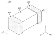
도 2는 본 발명의 일 실시형태에 따른 적층 세라믹 커패시터를 나타내는 개략적인 사시도이다.
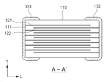
도 3은 도 2의 A-A'를 따라 취한 적층 세라믹 커패시터를 나타내는 개략적인 단면도이다.1 is a base material represented by the embodiment of the conventional BaTiO 3 with the base material powder represented by the first principal component and the second main component of PbTiO 3 (1-x) BaTiO 3 -xPbTiO 3 include represented by represented by BaTiO 3 (? T ) relative to the DC electric field and the rate of change of the dielectric constant in the comparative example using the powder.
2 is a schematic perspective view showing a multilayer ceramic capacitor according to one embodiment of the present invention.
3 is a schematic cross-sectional view showing a multilayer ceramic capacitor taken along line A-A 'in Fig.
이하, 첨부된 도면을 참조하여 본 발명의 바람직한 실시형태들을 설명한다.Hereinafter, preferred embodiments of the present invention will be described with reference to the accompanying drawings.
그러나, 본 발명의 실시형태는 여러 가지 다른 형태로 변형될 수 있으며, 본 발명의 범위가 이하 설명하는 실시 형태로 한정되는 것은 아니다. 또한, 본 발명의 실시형태는 당해 기술 분야에서 평균적인 지식을 가진 자에게 본 발명을 더욱 완전하게 설명하기 위해서 제공되는 것이다. 따라서, 도면에서의 요소들의 형상 및 크기 등은 명확한 설명을 위해 과장될 수 있으며, 도면상의 동일한 부호로 표시되는 요소는 동일한 요소이다.However, the embodiments of the present invention can be modified into various other forms, and the scope of the present invention is not limited to the embodiments described below. Further, the embodiments of the present invention are provided to more fully explain the present invention to those skilled in the art. Therefore, the shapes and sizes of the elements in the drawings and the like can be exaggerated for clarity, and the elements denoted by the same reference numerals in the drawings are the same elements.
본 발명은 유전체 자기 조성물에 관한 것으로, 유전체 자기 조성물을 포함하는 전자부품은 커패시터, 인덕터, 압전체 소자, 바리스터, 또는 서미스터 등이 있으며, 이하에서는 유전체 자기 조성물 및 전자부품의 일례로서 적층 세라믹 커패시터에 관하여 설명한다.BACKGROUND OF THE INVENTION 1. Field of the Invention The present invention relates to a dielectric ceramic composition, and an electronic component including the dielectric ceramic composition includes a capacitor, an inductor, a piezoelectric element, a varistor, or a thermistor. Hereinafter, the dielectric ceramic composition and the multilayer ceramic capacitor Explain.
본 발명의 일 실시 형태에 따른 유전체 자기 조성물은 BaTiO3로 표시되는 제1 주성분 및 PbTiO3로 표시되는 제2 주성분을 포함하는 (1-x)BaTiO3-xPbTiO3로 표시되는 모재 분말을 포함하며, 상기 x는 0.0025≤x≤0.4를 만족하고, 상기 모재 분말 100 몰%에 대하여, Ba을 포함하는 산화물, 탄산염 또는 불화물이며, 그 함량이 Ba at% 기준으로 0 내지 3.0 at%의 제4 부성분을 더 포함한다.The dielectric ceramic composition according to an embodiment of the present invention comprises a base metal powder represented by the first principal component and the second main component of PbTiO 3 (1-x) BaTiO 3 -xPbTiO 3 include represented by represented by BaTiO 3, and , X satisfies 0.0025? X? 0.4, and is an oxide, carbonate or fluoride including Ba in 100 mol% of the base material powder, and the content is 0 to 3.0 at% based on Ba at% .
본 발명의 일 실시형태에 따른 유전체 자기 조성물은 EIA(Electronic Industries Association) 규격에서 명시한 X5R(-55℃~85℃), X7R(-55℃~125℃), X8R(-55℃~150℃) 그리고, X9R(-55℃~200℃) 특성을 만족할 수 있다.(-55 ° C to 85 ° C), X7R (-55 ° C to 125 ° C) and X8R (-55 ° C to 150 ° C) specified in EIA (Electronic Industries Association) standards, The X9R (-55 ° C to 200 ° C) characteristics can be satisfied.
또한, 이를 이용한 적층 세라믹 커패시터를 제공하여 상기 온도 특성을 만족함과 동시에 우수한 신뢰성을 구현할 수 있다.Also, by providing a multilayer ceramic capacitor using the same, it is possible to satisfy the temperature characteristics and realize excellent reliability.
이하, 본 발명의 일 실시형태에 따른 유전체 자기 조성물의 각 성분을 보다 구체적으로 설명하도록 한다.Hereinafter, each component of the dielectric ceramic composition according to one embodiment of the present invention will be described in more detail.
a) 모재 분말a) Base material powder
본 발명의 일 실시형태에 따른 유전체 자기 조성물은 BaTiO3로 표시되는 제1 주성분 및 PbTiO3로 표시되는 제2 주성분을 포함하는 (1-x)BaTiO3-xPbTiO3로 표시되는 모재 분말을 포함한다. The dielectric ceramic composition according to an embodiment of the present invention comprises a base metal powder represented by the first principal component and the second main component of PbTiO 3 (1-x) BaTiO 3 -xPbTiO 3 include represented by represented by BaTiO 3 .
상기 식에서, x는 0.0025≤x≤0.4를 만족할 수 있다.In the above formula, x may satisfy 0.0025? X? 0.4.
상기 제1 주성분은 BaTiO3로 표시될 수 있으며, 상기 BaTiO3는 일반적인 유전체 모재에 사용되는 재료로서, 큐리 온도가 대략 125도 정도인 강유전체 재료이다.The first main component may be represented by BaTiO 3 , and the BaTiO 3 is a ferroelectric material having a Curie temperature of approximately 125 degrees.
또한, 상기 제2 주성분은 PbTiO3로 표시된다.The second main component is represented by PbTiO 3 .
상기 제2 주성분인 PbTiO3는 제1 주성분인 BaTiO3에 비하여 자발 분극의 크기가 크다.The second main component, PbTiO 3, has a larger spontaneous polarization than BaTiO 3 , which is the first main component.
다만, PbTiO3는 분역벽(Domain wall)의 이동도(Mobility)가 낮아 유전율이 낮은 문제가 있다.However, PbTiO 3 has a low dielectric constant due to low mobility of the domain wall.
일반적으로 강유전체가 높은 유전율을 가지기 위해서는 자발 분극의 크기가 크고 동시에 분역벽(Domain wall)의 이동도(Mobility)가 커서 이러한 분극들이 외부 전계 방향에 따라 쉽게 스위칭할 수 있어야 한다.Generally, in order for a ferroelectric substance to have a high dielectric constant, the spontaneous polarization has a large size and the mobility of the domain wall is large, so that the polarization can easily switch according to the external electric field direction.
본 발명의 일 실시형태에 따르면, BaTiO3로 표시되는 제1 주성분과 제1 주성분에 비해 자발 분극의 크기가 큰 PbTiO3로 표시되는 제2 주성분을 포함하되, 제2 주성분을 적정량 포함함으로써, 자발 분극의 크기를 크게 함과 동시에 분역벽(Domain wall)의 이동도(Mobility)를 향상시켜 BaTiO3로 표시되는 모재에 비해 보다 작은 결정립 크기에서도 높은 유전율을 구현할 수 있다.According to one embodiment of the present invention, there is provided a sputtering target comprising a first main component represented by BaTiO 3 and a second main component represented by PbTiO 3 having a larger spontaneous polarization than the first main component, It is possible to increase the size of the polarization and improve the mobility of the domain wall, thereby realizing a higher permittivity even at a smaller grain size than the base material represented by BaTiO 3 .
이로 인해, 유전율이 높으면서 동시에 DC-bias 특성이 우수한 유전체 자기 조성물을 구현할 수 있다.As a result, a dielectric ceramic composition having a high dielectric constant and excellent DC-bias characteristics can be realized.
즉, 본 발명의 일 실시형태에 따른 유전체 자기 조성물의 모재 분말은 BaTiO3로 표시되는 제1 주성분 및 PbTiO3로 표시되는 제2 주성분을 포함하는 (1-x)BaTiO3-xPbTiO3로 표시되되, 제2 주성분인 PbTiO3의 함량이 0.0025≤x≤0.4를 만족함으로써, 상기의 효과를 얻을 수 있다.That is, the dielectric base material powder of a ceramic composition according to an embodiment of the present invention doedoe represented by the first principal component and the second main component of PbTiO 3 (1-x) BaTiO 3 -xPbTiO 3 include represented by represented by BaTiO 3 , And the content of PbTiO 3 as the second main component satisfies 0.0025? X? 0.4, the above effect can be obtained.
상기 x가 0.0025 미만이면 DC-bias 특성이 나빠지는 문제가 있다.If x is less than 0.0025, there is a problem that the DC-bias characteristic is deteriorated.
한편, x가 0.4를 초과하면 상온 유전율이 3000 미만으로 낮아지는 문제가 ㅇ있다.On the other hand, when x exceeds 0.4, there is a problem that the dielectric constant at room temperature is lowered to less than 3000.
또한, 상기 유전체 자기 조성물의 모재 분말은 제1 주성분과 제2 주성분이 고용체 형태일 수도 있다.The base material powder of the dielectric ceramic composition may be in the form of a solid solution of the first main component and the second main component.
상기 모재 분말이 서로 고용된 형태일 경우에는 상기 모재 분말은 단일상 형태일 수 있으며, 유전율, 온도 특성, 정전용량 변화율(temperature coefficient of capacitance, TCC), DC-bias 특성 및 손실율 등이 두 재료가 혼합된 형태보다 우수할 수 있다.In the case where the mother material powders are solid-dissolved in each other, the mother material powder may be in the form of single phase, and the dielectric constant, the temperature characteristic, the temperature coefficient of capacitance (TCC), the DC bias characteristic, May be superior to the mixed form.
상기 모재 분말은 특별히 제한되는 것은 아니나, 분말의 평균 입경은 1000 nm 이하일 수 있다.The base material powder is not particularly limited, but the average particle diameter of the powder may be 1000 nm or less.
b)제1 부성분b) the first subcomponent
본 발명의 일 실시형태에 따르면, 상기 유전체 자기 조성물은 제1 부성분으로서, Mn, V, Cr, Fe, Ni, Co, Cu 및 Zn 중 적어도 하나 이상을 포함하는 산화물 혹은 탄산염을 더 포함할 수 있다. According to an embodiment of the present invention, the dielectric ceramic composition may further include, as a first accessory ingredient, an oxide or a carbonate including at least one of Mn, V, Cr, Fe, Ni, Co, Cu and Zn .
상기 제1 부성분으로서, Mn, V, Cr, Fe, Ni, Co, Cu 및 Zn 중 적어도 하나 이상을 포함하는 산화물 혹은 탄산염은 상기 모재 분말 100 몰%에 대하여, 0.1 내지 2.0 몰%의 함량으로 포함될 수 있다.The oxide or carbonate containing at least one of Mn, V, Cr, Fe, Ni, Co, Cu and Zn as the first accessory ingredient is contained in an amount of 0.1 to 2.0 mol% based on 100 mol% .
상기 제1 부성분은 유전체 자기 조성물이 적용된 적층 세라믹 커패시터의 소성 온도 저하 및 고온 내전압 특성을 향상시키는 역할을 한다.The first subcomponent serves to improve the sintering temperature lowering and the high temperature withstand voltage characteristics of the multilayer ceramic capacitor to which the dielectric ceramic composition is applied.
상기 제1 부성분의 함량 및 후술하는 제2 부성분의 함량은 모재 분말 100 몰%에 대하여 포함되는 양으로서, 특히 각 부성분이 포함하는 금속 이온의 몰%로 정의될 수 있다.The content of the first subcomponent and the content of the second subcomponent to be described later may be defined as the amount contained relative to 100 mol% of the base material powder, in particular, the mol% of metal ions contained in each subcomponent.
상기 제1 부성분의 함량이 0.1 몰% 미만이면 소성 온도가 높아지고 고온 내전압 특성이 다소 저하될 수 있다.If the content of the first subcomponent is less than 0.1 mol%, the firing temperature may increase and the high-temperature withstand voltage characteristic may be somewhat lowered.
상기 제1 부성분의 함량이 2.0 몰% 이상의 경우에는 고온 내전압 특성 및 상온 비저항이 저하될 수 있다.If the content of the first accessory ingredient is 2.0 mol% or more, high-temperature withstand voltage characteristics and room temperature resistivity may be lowered.
특히, 본 발명의 일 실시형태에 따른 유전체 자기 조성물은 모재 분말 100 몰%에 대하여 0.1 내지 2.0 몰%의 함량을 갖는 제1 부성분을 더 포함할 수 있으며, 이로 인하여 저온 소성이 가능하며 높은 고온 내전압 특성을 얻을 수 있다.In particular, the dielectric ceramic composition according to one embodiment of the present invention may further include a first subcomponent having a content of 0.1 to 2.0 mol% based on 100 mol% of the base material powder, thereby enabling low-temperature firing, Characteristics can be obtained.
c)제2 부성분c) second subcomponent
본 발명의 일 실시형태에 따르면, 상기 유전체 자기 조성물은 제2 부성분으로서, Si를 포함하는 산화물 또는 Si를 포함하는 글라스(Glass) 화합물을 포함할 수 있다. According to one embodiment of the present invention, the dielectric ceramic composition may include an oxide containing Si or a glass compound containing Si as the second subcomponent.
상기 유전체 자기 조성물은 상기 모재 분말 100 몰%에 대하여, Si를 포함하는 산화물 또는 Si를 포함하는 글라스(Glass) 화합물인 0.2 내지 5.0 몰%의 제2 부성분을 더 포함할 수 있다.The dielectric ceramic composition may further comprise an oxide containing Si or a second sub ingredient of 0.2 to 5.0 mol%, which is a glass compound containing Si, based on 100 mol% of the base material powder.
상기 제2 부성분은 유전체 자기 조성물이 적용된 적층 세라믹 커패시터의 소성 온도 저하 및 고온 내전압 특성을 향상시키는 역할을 한다.The second subcomponent serves to improve the sintering temperature lowering and the high temperature withstanding voltage characteristics of the multilayer ceramic capacitor to which the dielectric ceramic composition is applied.
상기 제2 부성분의 함량이 상기 모재 분말 100 몰%에 대하여, 0.2 몰% 미만이면 소성 온도가 높아질 수 있다.If the content of the second subcomponent is less than 0.2 mol% based on 100 mol% of the base material powder, the firing temperature may be increased.
상기 제2 부성분의 함량이 상기 모재 분말 100 몰%에 대하여, 5.0 몰% 이상의 경우에는 고온 내전압 특성이 저하될 수 있다.If the content of the second subcomponent is 5.0 mol% or more based on 100 mol% of the base material powder, the high-temperature withstand voltage characteristics may be deteriorated.
특히, 본 발명의 일 실시형태에 따른 유전체 자기 조성물은 상기 모재 분말 100 몰%에 대하여, 0.2 내지 5.0 몰%의 함량을 갖는 제2 부성분을 더 포함할 수 있으며, 이로 인하여 저온 소성이 가능하며 높은 고온 내전압 특성을 얻을 수 있다.In particular, the dielectric ceramic composition according to an embodiment of the present invention may further comprise a second subcomponent having a content of 0.2 to 5.0 mol% based on 100 mol% of the base material powder, High-withstand voltage characteristics can be obtained.
d)제3 부성분d) third subcomponent
본 발명의 일 실시형태에 따르면, 상기 유전체 자기 조성물은 Li를 포함하는 산화물, 탄산염 또는 불화물인 제3 부성분을 더 포함할 수 있다. According to one embodiment of the present invention, the dielectric ceramic composition may further comprise a third subcomponent which is an oxide, carbonate or fluoride including Li.
상기 유전체 자기 조성물은 상기 모재 분말 100 몰%에 대하여, Li를 포함하는 산화물, 탄산염 또는 불화물인 0.4 내지 12.0 몰%의 제3 부성분을 더 포함할 수 있다.The dielectric ceramic composition may further include 0.4 to 12.0 mol% of a third subcomponent of Li, an oxide, a carbonate or a fluoride, based on 100 mol% of the base material powder.
상기 제3 부성분은 유전체 자기 조성물이 적용된 적층 세라믹 커패시터의 소성 온도 저하 및 고온 내전압 특성을 향상시키는 역할을 한다.The third subcomponent serves to improve sintering temperature lowering and high-temperature withstand voltage characteristics of the multilayer ceramic capacitor to which the dielectric ceramic composition is applied.
또한, 상기 제3 부성분은 내부전극으로서 구리(Cu)를 사용한 경우에도 적층 세라믹 커패시터의 목표 특성을 얻을 수 있는 효과가 있다.Further, the third subcomponent has an effect of obtaining the target characteristics of the multilayer ceramic capacitor even when copper (Cu) is used as the internal electrode.
상기 제3 부성분의 함량이 상기 모재 분말 100 몰%에 대하여, 0.4 몰% 미만이면 소성 온도가 높아질 수 있으며, 유전율이 낮고 고온 내전압 특성이 저하될 수 있다.If the content of the third subcomponent is less than 0.4 mol% based on 100 mol% of the base material powder, the firing temperature may be high, and the dielectric constant may be low and the high-temperature withstand voltage characteristic may be deteriorated.
상기 제3 부성분의 함량이 상기 모재 분말 100 몰%에 대하여, 12.0 몰% 이상의 경우에는 이차상 생성 등으로 인해 고온 내전압 특성이 저하될 수 있다.When the content of the third subcomponent is 12.0 mol% or more with respect to 100 mol% of the base material powder, the high-temperature withstand voltage characteristic may be lowered due to secondary phase formation or the like.
특히, 본 발명의 일 실시형태에 따른 유전체 자기 조성물은 상기 모재 분말 100 몰%에 대하여, 0.4 내지 12.0 몰%의 함량을 갖는 제3 부성분을 더 포함할 수 있으며, 이로 인하여 구리(Cu)를 내부전극으로 사용할 수 있으며, 저온 소성이 가능하고 높은 고온 내전압 특성을 얻을 수 있다.In particular, the dielectric ceramic composition according to an embodiment of the present invention may further include a third subcomponent having an amount of 0.4 to 12.0 mol% based on 100 mol% of the base material powder, It can be used as an electrode, can be baked at a low temperature, and a high high-temperature withstand voltage characteristic can be obtained.
e)제4 부성분e) fourth subcomponent
본 발명의 일 실시형태에 따르면, 상기 유전체 자기 조성물은 Ba을 포함하는 산화물, 탄산염 또는 불화물인 제4 부성분을 더 포함할 수 있다. According to an embodiment of the present invention, the dielectric ceramic composition may further include a fourth subcomponent which is an oxide, a carbonate, or a fluoride including Ba.
상기 유전체 자기 조성물은 상기 모재 분말 100 몰%에 대하여, Ba을 포함하는 산화물, 탄산염 또는 불화물이며, 그 함량이 Ba at% 기준으로 0 내지 3.0 at%의 제4 부성분을 더 포함할 수 있다.The dielectric ceramic composition may further contain an oxide, carbonate or fluoride containing Ba in an amount of 0 to 3.0 at% based on Ba at% based on 100 mol% of the base material powder.
상기 제4 부성분은 유전체 자기 조성물이 적용된 적층 세라믹 커패시터의 유전율을 높이는 역할을 한다.The fourth subcomponent serves to increase the dielectric constant of the multilayer ceramic capacitor to which the dielectric ceramic composition is applied.
또한, 상기 제4 부성분은 내부전극으로서 구리(Cu)를 사용하고 환원 분위기(N2 분위기)에서 소성한 경우에도 적층 세라믹 커패시터의 목표 특성을 얻을 수 있는 효과가 있다.Also, the fourth subcomponent has an effect of obtaining the target characteristics of the multilayer ceramic capacitor even when copper (Cu) is used as the internal electrode and firing is performed in a reducing atmosphere (N 2 atmosphere).
상기 제4 부성분의 함량이 상기 모재 분말 100 몰%에 대하여, Ba at% 기준으로 3.0 at%를 초과하는 경우에는 고온 내전압 특성이 저하될 수 있다.If the content of the fourth subcomponent exceeds 3.0 at% based on Ba at% based on 100 mol% of the base material powder, the high-temperature withstand voltage characteristic may be lowered.
특히, 본 발명의 일 실시형태에 따른 유전체 자기 조성물은 상기 모재 분말 100 몰%에 대하여, Ba을 포함하는 산화물, 탄산염 또는 불화물이며, 그 함량이 Ba at% 기준으로 0 내지 3.0 at%의 제4 부성분을 더 포함할 수 있으며, 이로 인하여 구리(Cu)를 내부전극으로 사용할 수 있으며, 환원 분위기에서 소성이 가능하며, 높은 유전율과 우수한 고온 내전압 특성을 얻을 수 있다.In particular, the dielectric ceramic composition according to one embodiment of the present invention is an oxide, carbonate, or fluoride containing Ba in an amount of 0 to 3.0 at% based on 100 atom% of the base material powder, (Cu) can be used as an internal electrode, firing can be performed in a reducing atmosphere, high dielectric constant and excellent high temperature withstand voltage characteristics can be obtained.
한편, 본 발명의 일 실시형태에 따르면 상기 제4 부성분은 Ba/Si의 몰비가 0 내지 4.0을 만족하도록 Ba을 포함할 수 있다.Meanwhile, according to one embodiment of the present invention, the fourth subcomponent may include Ba so that the molar ratio of Ba / Si is 0 to 4.0.
Si를 포함하는 산화물 또는 Si를 포함하는 글라스(Glass) 화합물을 포함하는 제2 부성분과 상기 제4 부성분의 몰비가 0 내지 4.0을 만족하도록 조절함으로써, 높은 유전율을 얻음과 동시에 우수한 고온 내전압 특성을 얻을 수 있다.By controlling the molar ratio of the second subcomponent including the Si-containing oxide or the Si-containing glass subcomponent to the fourth subcomponent to be in the range of 0 to 4.0, a high dielectric constant can be obtained and excellent high-temperature withstand voltage characteristics can be obtained .
구체적으로, 상기 Ba을 포함하는 산화물, 탄산염 또는 불화물인 제4 부성분의 Ba 함량이 3.0 at%를 초과하는 경우에도 제2 부성분인 Si의 함량을 증가시켜 Ba/Si의 몰비가 4.0을 만족하도록 조절할 경우 고온 내전압 특성을 향상시킬 수 있다.Specifically, when the Ba content of the fourth subcomponent such as an oxide, a carbonate or a fluoride containing Ba is more than 3.0 at%, the content of Si as the second sub ingredient is increased to adjust the Ba / Si molar ratio to be 4.0 The high-temperature withstand voltage characteristics can be improved.
그러나, Ba/Si의 몰비가 4.0을 초과하는 경우에는 내전압 특성이 저하될 수 있고, 신뢰성에 문제가 생길 수 있다.However, when the molar ratio of Ba / Si exceeds 4.0, the withstand voltage characteristic may be lowered, which may cause reliability problems.
f)제5 부성분f) fifth subcomponent
본 발명의 일 실시형태에 따르면, 상기 유전체 자기 조성물은 Dy, Y, Ho, Sm, Gd, Er, La 및 Tb 중 적어도 하나를 포함하는 산화물, 탄산염 또는 불화물인 제5 부성분을 더 포함할 수 있다. According to an embodiment of the present invention, the dielectric ceramic composition may further comprise a fifth subcomponent which is an oxide, a carbonate or a fluoride including at least one of Dy, Y, Ho, Sm, Gd, Er, La and Tb .
상기 유전체 자기 조성물은 상기 모재 분말 100 몰%에 대하여, Dy, Y, Ho, Sm, Gd, Er, La 및 Tb 중 적어도 하나를 포함하는 산화물, 탄산염 또는 불화물이며, 그 함량이 각 원소 at% 기준으로 0 내지 4.0 at%의 제5 부성분을 더 포함할 수 있다.Wherein the dielectric ceramic composition is an oxide, carbonate or fluoride containing at least one of Dy, Y, Ho, Sm, Gd, Er, La and Tb relative to 100 mole% of the base material powder, , And 0 to 4.0 at% of a fifth subcomponent.
상기 제5 부성분은 유전체 자기 조성물이 적용된 적층 세라믹 커패시터의 DC-bias 특성을 개선하고, 고온 내전압을 증가시켜 신뢰성을 향상시키는 역할을 한다.The fifth subcomponent improves the DC-bias characteristic of the multilayer ceramic capacitor to which the dielectric ceramic composition is applied, and improves the reliability by increasing the high-temperature withstand voltage.
상기 제5 부성분의 함량이 상기 모재 분말 100 몰%에 대하여, 각 원소 at% 기준으로 4.0 at%를 초과하는 경우에는 상온 유전율이 감소하여 목표 특성 구현을 할 수 없다.If the content of the fifth subcomponent exceeds 4.0 at% based on 100 mol% of the base material powder, the room temperature dielectric constant decreases and the target characteristics can not be realized.
특히, 본 발명의 일 실시형태에 따른 유전체 자기 조성물은 상기 모재 분말 100 몰%에 대하여, Dy, Y, Ho, Sm, Gd, Er, La 및 Tb 중 적어도 하나를 포함하는 산화물, 탄산염 또는 불화물이며, 그 함량이 각 원소 at% 기준으로 0 내지 4.0 at%의 제5 부성분을 더 포함할 수 있으며, 이로 인하여 DC-bias 특성을 개선하고, 고온 내전압을 증가시켜 신뢰성을 향상시킬 수 있다.In particular, the dielectric ceramic composition according to one embodiment of the present invention is an oxide, carbonate or fluoride containing at least one of Dy, Y, Ho, Sm, Gd, Er, La and Tb with respect to 100 mol% , And a content of the fifth subcomponent of 0 to 4.0 at% based on the at% of each element, thereby improving the DC-bias characteristic and improving the reliability by increasing the high-temperature withstand voltage.
도 1은 BaTiO3로 표시되는 제1 주성분 및 PbTiO3로 표시되는 제2 주성분을 포함하는 (1-x)BaTiO3-xPbTiO3로 표시되는 모재 분말을 이용한 실시예와 종래 BaTiO3로 표시되는 모재 분말을 이용한 비교예의 DC 전계 대비 유전율(εT)과 유전율의 변화율을 나타내는 그래프이다.1 is a base material represented by the embodiment of the conventional BaTiO 3 with the base material powder represented by the first principal component and the second main component of PbTiO 3 (1-x) BaTiO 3 -xPbTiO 3 include represented by represented by BaTiO 3 (? T ) relative to the DC electric field and the rate of change of the dielectric constant in the comparative example using the powder.
도 1을 참조하면, 큐리 온도가 125℃인 BaTiO3 상용 X5R 유전체 재료를 적용한 비교예에 비해 본 발명의 실시예인 BaTiO3로 표시되는 제1 주성분 및 PbTiO3로 표시되는 제2 주성분을 포함하는 (1-x)BaTiO3-xPbTiO3로 표시되는 모재 분말을 이용한 경우, DC-bias 특성이 우수함을 알 수 있다.Referring to Figure 1, a second principal component represented by the first principal component, and PbTiO 3 has Curie temperature represented by 125 ℃ of BaTiO 3 commercial X5R embodiment of the present invention compared to the comparative example in which the dielectric material, BaTiO 3 ( 1-x) BaTiO 3 -xPbTiO 3 , the DC-bias characteristic is excellent.
도 2는 본 발명의 일 실시형태에 따른 적층 세라믹 커패시터(100)를 나타내는 개략적인 사시도이고, 도 3은 도 2의 A-A'를 따라 취한 적층 세라믹 커패시터(100)를 나타내는 개략적인 단면도이다.FIG. 2 is a schematic perspective view showing a multilayer
도 2 및 도 3을 참조하면, 본 발명의 다른 실시예에 따른 적층 세라믹 커패시터(100)는 유전체층(111)과 제1 및 제2 내부 전극(121, 122)이 교대로 적층된 세라믹 본체(110)를 가진다. 세라믹 본체(110)의 양 단부에는 세라믹 본체(110)의 내부에 교대로 배치된 제1 및 제2 내부 전극(121, 122)과 각각 도통하는 제1 및 제2 외부 전극(131, 132)이 형성되어 있다.2 and 3, a multilayer
세라믹 본체(110)의 형상에 특별히 제한은 없지만, 일반적으로 육면체 형상일 수 있다. 또한, 그 치수도 특별히 제한은 없고, 용도에 따라 적절한 치수로 할 수 있고, 예를 들면 (0.6∼5.6mm)×(0.3∼5.0mm)×(0.3∼1.9mm)일 수 있다.The shape of the
유전체층(111)의 두께는 커패시터의 용량 설계에 맞추어 임의로 변경할 수 있는데, 본 발명의 일 실시예에서 소성 후 유전체층의 두께는 1층당 바람직하게는 0.2㎛ 이상일 수 있다. The thickness of the dielectric layer 111 may be arbitrarily changed in accordance with the capacity design of the capacitor. In one embodiment of the present invention, the thickness of the dielectric layer after firing may be preferably 0.2 m or more per layer.
너무 얇은 두께의 유전체층은 한층 내에 존재하는 결정립 수가 작아 신뢰성에 나쁜 영향을 미치기 때문에 유전체층의 두께는 0.2 ㎛ 이상일 수 있다.The dielectric layer having too thin a thickness has a small number of crystal grains existing in one layer and adversely affects the reliability, so that the thickness of the dielectric layer can be 0.2 탆 or more.
제1 및 제2 내부 전극(121, 122)은 각 단면이 세라믹 본체(110)의 대향하는 양 단부의 표면에 교대로 노출되도록 적층되어 있다. The first and second
상기 제1 및 제2 외부 전극(131, 132)은 세라믹 본체(110)의 양 단부에 형성되고, 교대로 배치된 제1 및 제2 내부 전극(121, 122)의 노출 단면에 전기적으로 연결되어 커패시터 회로를 구성한다.The first and second
상기 제1 및 제2 내부 전극(121, 122)에 함유되는 도전성 재료는 특별히 한정되지 않지만, 본 발명의 일 실시형태에서는 팔라듐(Pd), 구리(Cu) 혹은 니켈(Ni)을 이용할 수 있다.The conductive material contained in the first and second
상기 제1 및 제2 내부 전극(121, 122)의 두께는 용도 등에 따라 적절히 결정할 수 있으며 특별히 제한되는 것은 아니나, 예를 들면 0.1 내지 5㎛ 또는 0.1∼2.5㎛일 수 있다.The thickness of the first and second
상기 제1 및 제2 외부 전극(131, 132)에 함유되는 도전성 재료는 특별히 한정되지 않지만, 니켈(Ni), 구리(Cu), 또는 이들 합금을 이용할 수 있다. The conductive material contained in the first and second
상기 제1 및 제2 외부 전극(131, 132)의 두께는 용도 등에 따라 적절히 결정할 수 있으며 특별히 제한되는 것은 아니나, 예를 들면 10 내지 50㎛ 일 수 있다.The thickness of the first and second
상기 세라믹 본체(110)를 구성하는 유전체층(111)은 본 발명의 일 실시형태에 따른 유전체 자기 조성물을 포함할 수 있다.The dielectric layer 111 constituting the
상기 유전체 자기 조성물은 BaTiO3로 표시되는 제1 주성분 및 PbTiO3로 표시되는 제2 주성분을 포함하는 (1-x)BaTiO3-xPbTiO3로 표시되는 모재 분말을 포함하며, 상기 x는 0.0025≤x≤0.4를 만족하고, 상기 모재 분말 100 몰%에 대하여, Ba을 포함하는 산화물, 탄산염 또는 불화물이며, 그 함량이 Ba at% 기준으로 0 내지 3.0 at%의 제4 부성분을 더 포함할 수 있다.And said dielectric ceramic composition comprises a base metal powder represented by the first principal component and the second main component of PbTiO 3 (1-x) BaTiO 3 -xPbTiO 3 include represented by represented by BaTiO 3, wherein x is 0.0025≤x ? 0.4, and the fourth sub ingredient is an oxide, carbonate or fluoride containing Ba in an amount of 0 to 3.0 at% based on Ba at% based on 100 mol% of the base material powder.
상기 유전체 자기 조성물에 대한 구체적인 설명은 상술한 본 발명의 일 실시형태에 따른 유전체 자기 조성물의 특징과 동일하므로 여기서는 생략하도록 한다.A detailed description of the dielectric ceramic composition is the same as that of the dielectric ceramic composition according to the embodiment of the present invention described above, and thus will not be described here.
이하, 실시예 및 비교예를 통하여 본 발명을 더욱 상세히 설명하지만, 이는 발명의 구체적인 이해를 돕기 위한 것으로 본 발명의 범위가 실시예에 의해 한정되는 것은 아니다.Hereinafter, the present invention will be described in more detail with reference to examples and comparative examples, but it is to be understood that the scope of the present invention is not limited by the examples.
원료 분말은 (1-x)BaTiO3-xPbTiO3을 주성분으로 하며, 평균 입자 크기가 300 nm인 주성분 분말을 사용하였다.As the raw material powder, a main component powder having (1-x) BaTiO 3 -xPbTiO 3 as a main component and having an average particle size of 300 nm was used.
하기 표 1 및 3에 기재된 조성비에 맞게 이들을 에탄올과 톨루엔을 용매로 하여 분산제와 함께 혼합한 후, 바인더를 혼합하여 세라믹 시트를 제작하였다.The mixture was mixed with a dispersant using ethanol and toluene as a solvent in accordance with the composition ratios shown in Tables 1 and 3, and then a binder was mixed to prepare a ceramic sheet.
하기 표 1에 기재된 조성에 의해 성형된 세라믹 시트에는 팔라듐(Pd) 내부전극을 인쇄하고, 표 3에 기재된 조성에 의해 성형된 세라믹 시트에는 구리(Cu) 내부전극을 인쇄하였다. Palladium (Pd) internal electrodes were printed on the ceramic sheets formed by the compositions shown in Table 1 below, and copper (Cu) internal electrodes were printed on the ceramic sheets formed by the composition shown in Table 3. [
상하 커버층으로는 10 내지 13㎛의 두께를 갖는 성형 시트로 25층으로 적층하였고, 약 2.0㎛의 두께를 갖는 내부전극이 인쇄된 시트를 21층 적층하여 액티브 층을 제작하여 바를 제조하였다. As the upper and lower cover layers, 25 sheets were laminated with a forming sheet having a thickness of 10 to 13 mu m, and 21 sheets of internal electrodes printed with a thickness of about 2.0 mu m were laminated to form an active layer to produce bars.
압착바는 절단기를 이용하여 3216(길이×폭×두께가 3.2mm×1.6mm×1.6mm) 크기의 칩으로 절단하였다. The compression bar was cut into chips of 3216 (length x width x thickness 3.2 mm x 1.6 mm x 1.6 mm) using a cutter.
제작이 완료된 칩을 가소한 뒤에 하기 표 1에 해당하는 시편들에 대해서는 대기 중에서(Air 분위기) 1180 ~ 1250℃의 온도 범위에서 소성을 진행하고, 표 3에 해당하는 시편들에 대해서는 환원 분위기(0.1% H2/99.9% N2, H2O/H2/N2 분위기)에서 940 ~ 980℃의 온도 범위에서 소성을 진행하였다.After firing the chips, the samples were subjected to firing in a temperature range of 1180 to 1250 ° C in the air (air atmosphere) for the specimens corresponding to the following Table 1, and in a reducing atmosphere (0.1 % H 2 / 99.9% N 2 , H 2 O / H 2 / N 2 atmosphere) at a temperature range of 940 to 980 ° C.
소성된 칩에 대하여 구리(Cu) 페이스트로 터미네이션 공정 및 전극 소성을 거쳐 외부전극을 완성하였다.The fired chip was subjected to a termination process and electrode firing with copper (Cu) paste to complete an external electrode.
상기와 같이 완성된 프로토 타입 적층 세라믹 커패시터(Proto-type MLCC) 시편에 대해 용량, DF, 절연저항, TCC 및 고온 150℃에서 전압 step 증가에 따른 저항 열화 거동 등을 평가하였다.The resistance deterioration behavior of the prototype multilayer ceramic capacitor (Proto-type MLCC) as described above was evaluated in terms of capacitance, DF, insulation resistance, TCC, and voltage step at high temperature of 150 ° C.
적층 세라믹 커패시터(MLCC) 칩의 상온 정전 용량 및 유전 손실은 LCR-meter를 이용하여 1 kHz, AC 0.5 V/㎛ 조건에서 용량을 측정하였다.The capacitance and dielectric loss of the multilayer ceramic capacitor (MLCC) chip were measured at 1 kHz and AC 0.5 V / ㎛ using LCR-meter.
정전 용량과 적층 세라믹 커패시터(MLCC) 칩의 유전체 두께, 내부전극 면적, 적층수로부터 적층 세라믹 커패시터(MLCC) 칩의 유전율을 계산하였다.The dielectric constant of the multilayer ceramic capacitor (MLCC) chip was calculated from the capacitance, the dielectric thickness of the multilayer ceramic capacitor (MLCC) chip, the internal electrode area, and the number of layers.
상온 절연 저항(IR)은 10 개씩의 샘플을 취하여 DC 10 V/㎛ 를 인가한 상태에서 60초 경과 후 측정하였다.The room temperature insulation resistance (IR) was measured after 60 seconds with 10 samples of 10 V / ㎛ applied.
온도에 따른 정전용량의 변화는 -55℃에서 125℃의 온도 범위에서 측정되었다.The change in capacitance with temperature was measured at a temperature range of -55 ° C to 125 ° C.
고온 IR 승압 실험은 150℃에서 전압 단계를 5 V/㎛ 씩 증가시키면서 저항 열화 거동을 측정하였는데, 각 단계의 시간은 10분이며 5초 간격으로 저항값을 측정하였다.The resistance IR degradation behavior was measured by increasing the voltage step by 5 V / ㎛ at 150 ℃. The resistance time was 10 minutes and the resistance value was measured every 5 seconds.
고온 IR 승압 실험으로부터 고온 내전압을 도출하였는데, 이는 소성 후 7㎛ 두께의 20층의 유전체를 가지는 3216 크기 칩에서 150℃에서 전압 스텝(Voltage step) dc 5 V/㎛를 10분간 인가하고 이 전압 스텝을 계속 증가시키면서 측정할 때, IR이 105Ω 이상을 견디는 전압을 의미한다.A high voltage withstand voltage was obtained from a high temperature IR voltage boosting test. After the firing, a voltage step dc of 5 V / 탆 was applied for 10 minutes at 150 ° C in a 3216 size chip having a 20- Means the voltage at which the IR will withstand more than 10 5 Ω when measured continuously.
RC 값은 AC 0.5 V/㎛, 1 kHz에서 측정한 상온 용량값과 DC 10 V/㎛ 에서 측정한 절연 저항값의 곱이다.RC value is the product of the room temperature capacity value measured at AC 0.5 V / 탆, 1 kHz and the insulation resistance value measured at DC 10 V / 탆.
유전체의 미세구조는 SEM(Scanning Electron Microscopy) 이미지로 관찰하였으며, 이로부터 결정립의 크기를 산출하였다.The microstructure of the dielectric was observed by SEM (Scanning Electron Microscopy) image, and the size of the grain was calculated from it.

아래 표 2는 상기 표 1에 명시된 조성에 해당하는 프로토 타입 적층 세라믹 커패시터(Proto-type MLCC) 칩의 특성을 나타낸다.Table 2 below shows the characteristics of a prototype multilayer ceramic capacitor (Proto-type MLCC) chip corresponding to the composition shown in Table 1 above.

상기 표 1을 참조하면, 실험예 1~11은 주성분 (1-x)BaTiO3+xPbTiO3 100 mol 대비 제1 부성분 MnO2의 함량이 0.5 mol, 제2 부성분 SiO2의 함량이 0.5 mol 일 때 제1 주성분 함량 (1-x) 및 제2 주성분 함량 x에 따른 실험예를 나타내고, 표 2의 실험예 1~11은 이에 해당하는 Pd-내부전극을 적용하고 대기중 (Air 분위기)에서 소성한 Proto-type 적층 세라믹 커패시터 샘플의 특성을 나타낸다. Referring to Table 1, in Experimental Examples 1 to 11, when the content of the first subcomponent MnO 2 was 0.5 mol and the content of the second subcomponent SiO 2 was 0.5 mol with respect to 100 mol of the main component (1-x) BaTiO 3 + xPbTiO 3 Experimental examples according to the first main component content (1-x) and the second main component content x are shown in Table 2, and in Experimental Examples 1 to 11 in Table 2, the corresponding Pd-internal electrodes were applied and fired in air Proto-type multilayer ceramic capacitor samples.
PbTiO3 함량 x가 증가함에 따라 결정립의 크기가 작아지다가 일정해지는 경향을 나타내며, 상온 유전율은 비교적 일정한 값을 유지하다가 감소하는 경향을 확인할 수 있다. As the content x of PbTiO 3 increases, the grain size tends to become smaller and become constant, and the room temperature dielectric constant tends to decrease while maintaining a relatively constant value.
PbTiO3가 첨가되지 않은 실험예 1의 경우 상온 유전율은 5624 수준으로 비교적 높게 구현되나 결정립의 크기가 1.8μm 수준으로 커서 dc-bias 변화율이 -66.0% 수준으로 문제가 있음을 알 수 있다. In the case of Experimental Example 1 in which PbTiO 3 is not added, the dielectric constant at room temperature is relatively high at 5624, but the grain size is as large as 1.8 μm, which indicates that the dc-bias change rate is at a level of -66.0%.
반면에, PbTiO3의 함량 x가 0.05인 실험예 6번의 경우 실험예 1번에 비해 동등 이상의 상온 유전율 5732를 나타내면서 결정립의 크기가 0.3μm로 작아 dc-bias 특성이 -32.7%로 매우 양호한 특성이 구현되는 것을 확인할 수 있다.On the other hand, in case of Experimental Example 6 in which the content x of PbTiO 3 is 0.05, the dielectric constant is 5732 which is equal to or higher than that of Experimental Example 1, and the crystal grain size is as small as 0.3 탆 and the dc-bias characteristic is -32.7% It can be confirmed that it is implemented.
PbTiO3의 함량 x가 0.4 이상으로 지나치게 과량인 실험예 11의 경우에는 상온 유전율이 3000 미만으로 낮아지는 문제가 있다. In the case of Experimental Example 11 in which the content x of PbTiO 3 is excessively larger than 0.4, there is a problem that the room temperature dielectric constant is lowered to less than 3000.
PbTiO3 함량 x가 0.005 (실험예3) ~ 0.3 (실험예10)의 범위에서 본 발명의 목표 특성인 상온 유전율: 3000 이상, RC값: 1000 Ohm-F 이상, TCC(125℃): ±15% 미만, dc-bias 변화율: ±50% 미만, 고온(150℃) 내전압: 50V/um 이상의 동시 구현이 가능함을 알 수 있다. A room temperature dielectric constant of 3000 or more, a RC value of 1000 Ohm-F or more, and a TCC (125 ° C) of ± 15 ° C, which are target characteristics of the present invention in the range of PbTiO 3 content x of 0.005 (Experimental Example 3) %, Dc-bias change rate: less than ± 50%, high temperature (150 ° C) withstand voltage: more than 50 V / um.
표 1의 실험예 12~17은 제1 주성분 함량 (1-x)가 0.95이고, 제2 주성분 x가 0.05이며, 주성분 (1-x)BaTiO3+xPbTiO3 100 mol 대비 제1 부성분 MnO2의 함량이 0.5 mol, 제2 부성분 SiO2의 함량이 0.5 mol 일때, 제1 부성분 Mn 함량에 따른 실험예를 나타내고, 표 2의 실험예 12~17은 이에 해당하는 Pd-내부전극을 적용하고 대기중 (Air 분위기)에서 소성한 Proto-type 적층 세라믹 커패시터 샘플의 특성을 나타낸다. Experiment shown in Table 1 Examples 12 to 17 has a first principal component content (1-x) 0.95, and the second main component is the x is 0.05, the main component (1-x) BaTiO 3 + xPbTiO 3 100 mol contrast of the first subcomponent MnO 2 Experimental examples according to the first sub ingredient Mn content are shown below when the content is 0.5 mol and the content of the second subcomponent SiO 2 is 0.5 mol. In Experimental Examples 12 to 17 of Table 2, a corresponding Pd-internal electrode is applied, Lt; RTI ID = 0.0 > (air atmosphere). ≪ / RTI >
제1 부성분 Mn의 함량이 0 인 경우 (실험예 12) RC값 및 고온(150℃) 내전압이 매우 낮은 문제가 있으며, 반면에 실험예 17과 같이 Mn의 함량이 3 mol로 지나치게 과량인 경우에는 상온 유전율이 3000 미만으로 낮아지는 문제가 있다. When the content of the first accessory constituent Mn is 0 (Experimental Example 12), the RC value and the high temperature (150 ° C) withstand voltage are very low. On the other hand, when the content of Mn is excessively high There is a problem that the dielectric constant at room temperature is lowered to less than 3000.
Mn 함량이 0.1 (실험예 12) ~ 2.0 (실험예 16)인 범위에서 본 발명의 목표 특성 구현이 가능함을 확인할 수 있다. It can be confirmed that the target characteristics of the present invention can be realized in the range of Mn content of 0.1 (Experimental Example 12) to 2.0 (Experimental Example 16).
표 1의 실험예 18~23은 제1 부성분에서 MnO2의 일부를 V2O5로 변경하거나 MnO2 전부를 V2O5로 변경하여 첨가했을 때의 실험예를 나타내고, 표 2의 실험예 18~23은 해당하는 Proto-type 칩의 특성을 나타낸다. Experiment of Table 1 Examples 18-23 indicates the experimental example used for a change to a part of the MnO 2 in the first subcomponent as V 2 O 5, or added to change the MnO 2 all as V 2 O 5, the experiment of Table 2, Example 18-23 show the characteristics of the corresponding Proto-type chip.
제1 부성분에서 Mn 혹은 V 등 종류에 상관없이 atomic % 기준으로 그 함량이 동일하면 거의 동일한 특성이 구현되는 것을 확인할 수 있다. It can be confirmed that substantially the same characteristics are realized when the contents of the first subcomponent are equal to each other based on atomic% irrespective of the kind of Mn or V and the like.
제1 부성분의 함량이 atomic % 기준으로 0.5 at%인 실험예 6, 18, 21의 특성이 거의 동일하며, 2.0 at% 인 실험예 16, 19, 22의 특성 또한 거의 동일함을 확인할 수 있다. It can be confirmed that the characteristics of Experimental Examples 6, 18 and 21 having the first subcomponent of 0.5 at% based on atomic% are almost the same, and the characteristics of Experiments 16, 19 and 22 having 2.0 at% are almost the same.
그리고, 제1 부성분의 함량이 atomic % 기준으로 3.0 at%으로 지나치게 과량인 실험예 17, 20, 23의 경우에는 모두 상온 유전율이 3000 미만인 문제가 발생한다.In the case of Experimental Examples 17, 20 and 23 in which the content of the first subcomponent is excessively high at 3.0 atomic% on the basis of atomic%, there arises a problem that the room temperature dielectric constant is less than 3000 at all.
따라서, 제1 부성분 전이금속 원소의 적정 함량은 원소비로 0.1 ~ 2.0 at%라고 기술할 수 있다.Therefore, the optimum content of the first sub-component transition metal element can be described as 0.1 to 2.0 at% in the original consumption.
표 1의 실험예 24~29는 제1 주성분 함량 (1-x)가 0.95이고, 제2 주성분 x가 0.05이며, 주성분 (1-x)BaTiO3+xPbTiO3 100 mol 대비 제1 부성분 MnO2의 함량이 0.5 mol일 때 제2 부성분 SiO2 함량 변화에 따른 실험예를 나타내고, 표 2의 실험예 24~29는 이에 해당하는 Pd-내부전극을 적용하고 대기중 (Air 분위기)에서 소성한 Proto-type 적층 세라믹 커패시터 샘플의 특성을 나타낸다. In Experimental Examples 24 to 29 of Table 1, the first main component (1-x) is 0.95, the second main component x is 0.05, and the first subcomponent MnO 2 (1-x) BaTiO 3 + xPbTiO 3 Experimental examples according to the second subcomponent SiO 2 content change when the content is 0.5 mol are shown in Table 2. Experimental Examples 24 to 29 of Table 2 show that the Pd- type laminated ceramic capacitor samples.
제2 부성분 SiO2 함량이 0 mol 인 경우에는(실험예 24), 소결성이 저하되어 유전율 및 고온 내전압 특성이 매우 낮은 문제가 있다. When the SiO 2 content of the second accessory constituent is 0 mol (Experimental Example 24), there is a problem that the sinterability is lowered and the dielectric constant and high-temperature withstand voltage characteristics are extremely low.
반면에, SiO2의 함량이 7 mol로 지나치게 과량인 경우에도(실험예 29), 상온유전율 및 고온 내전압 특성이 낮은 문제가 발생함을 알 수 있다.On the other hand, even when the content of SiO 2 is excessively large (7 moles) (Experiment 29), it can be seen that the room temperature dielectric constant and high-temperature withstanding voltage characteristics are low.
제2 부성분 SiO2 함량이 0.2 ~ 5.0 mol 범위에 해당하는 실험예 25~28에서는 본 발명의 목표 특성을 구현할 수 있음을 확인할 수 있다.It can be seen that the target characteristics of the present invention can be realized in Experimental Examples 25 to 28 in which the SiO 2 content of the second accessory ingredient is in the range of 0.2 to 5.0 mol.
따라서, 제2 부성분 원소의 적정 함량은 Si 원소비로 0.1 ~ 2.0 at% 라고 할 수 있다.Therefore, the optimum content of the second subcomponent element may be 0.1 to 2.0 at% in Si source consumption.

아래 표 4는 상기 표 3에 명시된 조성에 해당하는 프로토 타입 적층 세라믹 커패시터(Proto-type MLCC) 칩의 특성을 나타낸다.Table 4 below shows the characteristics of the prototype multilayer ceramic capacitor (Proto-type MLCC) chip corresponding to the composition shown in Table 3 above.

표 3의 실험예 30~36은 제1 주성분 함량 (1-x)가 0.95이고, 제2 주성분 x가 0.05이며, 주성분 (1-x)BaTiO3+xPbTiO3 100 mol 대비 제1 부성분 MnO2의 함량이 0.5 mol, 제2 부성분 SiO2의 함량이 0.5 mol 일 때, 제3 부성분 Li2CO3 함량 변화에 따른 실험예를 나타내고, 표 4의 실험예 30~36은 Cu 내부전극을 적용하고 N2 분위기에서 950℃에서 소성한 Proto-type 적층 세라믹 커패시터 샘플의 특성을 나타낸다.Experiment shown in Table 3 Examples 30 to 36 has a first principal component content (1-x) 0.95, and the second main component is the x is 0.05, the main component (1-x) BaTiO 3 + xPbTiO 3 100 mol contrast of the first subcomponent MnO 2 Experimental examples according to the content of the third subcomponent Li 2 CO 3 are shown in the case where the content is 0.5 mol and the content of the second subcomponent SiO 2 is 0.5 mol. In Experimental Examples 30 to 36 of Table 4, 2 shows the characteristics of a Proto-type multilayer ceramic capacitor sample fired at 950 ° C.
Li2CO3의 함량이 0.05 mol 과 같이 소량인 경우(실험예 30), 950℃ 소성시 소결성이 저하되어 유전율이 3000 미만으로 낮고, 고온 내전압이 50V/um 미만으로 낮아지는 문제가 있다.When the content of Li 2 CO 3 is as small as 0.05 mol (Experimental Example 30), there is a problem that the sinterability is lowered at 950 ° C. baking, the dielectric constant is lower than 3000, and the high-temperature withstand voltage is lowered to less than 50 V / μm.
반면에, Li2CO3의 함량이 8 mol로 지나치게 과량인 경우에는 이차상 생성 등으로 인해 역시 고온 내전압이 50V/um 미만으로 낮은 문제가 발생한다On the other hand, when the content of Li 2 CO 3 is excessively high (8 mol), the problem of low withstand voltage of 50 V /
Li2CO3 함량이 0.2 (실험예 31) ~ 6 mol (실험예 35)의 범위에 해당 되면, Cu 내부전극을 적용하면서 본 발명의 목표 특성 구현이 가능함을 확인할 수 있다It can be confirmed that when the Li 2 CO 3 content is in the range of 0.2 (Experimental Example 31) to 6 mol (Experimental Example 35), the target characteristics of the present invention can be realized while applying the Cu internal electrode
표 3의 실험예 37~43은 제3 부성분 LiF 함량 변화에 따른 실험예를 나타내고, 표 4의 실험예 37~43은 Cu 내부전극을 적용하고 N2 분위기에서 950℃에서 소성한 Proto-type 칩의 특성을 나타낸다.Experimental Examples 37 to 43 in Table 3 show experimental examples according to the change in the LiF content of the third subcomponent. Experimental Examples 37 to 43 in Table 4 show that the Proto-type chip obtained by applying a Cu internal electrode and firing at 950 캜 in an N 2 atmosphere .
Li의 함량이 at % 기준으로 동일하면 Li2CO3를 적용한 경우와 LiF를 적용한 경우의 특성이 거의 동일하게 구현되는 것을 확인할 수 있다(실험예 30과 37, 32와 39, 34와 41, 35와 42, 36과 43이 각각 이 경우에 해당됨).If the Li content is equal to at%, it can be confirmed that the characteristics of the case where Li 2 CO 3 is applied and the case where LiF is applied are almost the same (Experiments 30 and 37, 32 and 39, 34 and 41 and 35 And 42, 36 and 43 respectively correspond to this case).
따라서, Ni 내부전극뿐만 아니라 Cu 내부전극을 적용하면서 본 발명의 목표특성을 구현할 수 있는 제3 부성분의 적정 함량은 Li 원소비로 0.4 ~ 12 mol% 라고 할 수 있다.Therefore, the optimum content of the third subcomponent, which can realize the target characteristic of the present invention while applying the Cu internal electrode as well as the Ni internal electrode, can be 0.4 to 12 mol% in terms of the Li source consumption.
표 3의 실험예 44~50은 제1 주성분 함량 (1-x)가 0.95이고, 제2 주성분 x가 0.05이며, 주성분 (1-x)BaTiO3+xPbTiO3 100 mol 대비 제1 부성분 MnO2의 함량이 0.5 mol, 제2 부성분 SiO2의 함량이 0.5 mol 일 때, 제3 부성분 LiF의 함량이 2.0 mol 일 때, 제4 부성분 Ba의 함량 변화에 따른 실험예를 나타내고, 표 4의 실험예 44~50은 Cu 내부전극을 적용하고 N2 분위기에서 950℃에서 소성한 Proto-type 적층 세라믹 커패시터 샘플의 특성을 나타낸다.In Experimental Examples 44 to 50 of Table 3, the first main component (1-x) was 0.95, the second main component x was 0.05, and the first subcomponent MnO 2 (100) relative to 100 mol of the main component (1-x) BaTiO 3 + x PbTiO 3 An experimental example according to a change in the content of the fourth subcomponent Ba when the content of the second subcomponent SiO 2 is 0.5 mol and the content of the third subcomponent LiF is 2.0 mol is shown in Table 4, ~ 50 shows the characteristics of a Proto-type multilayer ceramic capacitor sample with a Cu internal electrode applied and fired at 950 ° C in an N 2 atmosphere.
Ba의 함량이 증가함에 따라 칩의 유전율이 증가하는 것을 확인할 수 있다. 그런데 제4 부성분 BaCO3의 함량이 3.0 mol로 과량인 경우에는 (실험예 49) 고온 내전압이 낮은 문제가 있다.As the content of Ba increases, the dielectric constant of the chip increases. However, when the content of the fourth subcomponent BaCO 3 is excessively increased to 3.0 mol (Example 49), there is a problem in that the high withstand voltage is low.
그러나, 제2 부성분 Si의 함량을 증가시켜 Ba/Si의 몰비를 4.0으로 조정하는 경우 (실험예 50) 고온 내전압 특성이 개선되어 본 발명의 목표 구현이 가능함을 알 수 있다.However, when the content of the second subcomponent Si is increased to adjust the molar ratio of Ba / Si to 4.0 (Experiment 50), high-temperature withstand voltage characteristics are improved, and it can be understood that the present invention can be achieved.
따라서, 제4 부성분 원소 Ba의 적정 함량 범위는 원소비로 0.0 내지 3.0 at%이고, Ba/Si 몰비는 4.0 이하임을 알 수 있다.Therefore, it can be seen that the optimum content range of the fourth subcomponent element Ba is 0.0 to 3.0 at% in terms of the original consumption and the Ba / Si molar ratio is 4.0 or less.
표 3의 실험예 51~57은 제1 주성분 함량 (1-x)가 0.95이고, 제2 주성분 x가 0.05이며, 주성분 (1-x)BaTiO3+xPbTiO3 100 mol 대비 제1 부성분 MnO2의 함량이 0.5 mol, 제2 부성분 SiO2의 함량이 0.5 mol 일 때, 제3 부성분 LiF의 함량이 2.0 mol, 제4 부성분 BaCO3의 함량이 0.75 mol 일 때, 제5 부성분 Dy의 함량 변화에 따른 실험예를 나타내고, 표 4의 실험예 51~57은 Cu 내부전극을 적용하고 N2 분위기에서 950℃에서 소성한 Proto-type 적층 세라믹 커패시터 샘플의 특성을 나타낸다.In Experimental Examples 51 to 57 of Table 3, the first main component (1-x) is 0.95, the second main component x is 0.05, and the first subcomponent MnO 2 is used as the main component (1-x) BaTiO 3 + xPbTiO 3 When the content of the third subcomponent LiF is 2.0 mol and the content of the fourth subcomponent BaCO 3 is 0.75 mol when the content of the second subcomponent SiO 2 is 0.5 mol and the content of the fifth subcomponent Dy is changed Experimental Examples 51 to 57 of Table 4 show the characteristics of a Proto-type multilayer ceramic capacitor sample obtained by applying a Cu internal electrode and firing at 950 ° C in an N 2 atmosphere.
제5 부성분 Dy2O3의 함량이 증가함에 따라 DC-bias 특성이 개선되고 고온 내전압이 증가하는 것을 확인할 수 있다. 따라서, 희토류 원소 Dy의 첨가가 적층 세라믹 커패시터의 신뢰성 개선에 효과가 있음을 알 수 있다.As the content of the fifth subcomponent Dy 2 O 3 is increased, the DC-bias characteristic is improved and the high-temperature withstand voltage is increased. Therefore, it can be seen that the addition of the rare earth element Dy is effective for improving the reliability of the multilayer ceramic capacitor.
그러나, 제5 부성분 Dy2O3의 함량이 4.0 mol로 과량인 경우에는 (실험예 57) 상온 유전율이 감소하여 3000 이하의 값을 가지므로, 목표 특성 구현이 안되는 문제가 있다.However, when the content of the fifth subcomponent Dy 2 O 3 is excessively increased to 4.0 mol (Example 57), the dielectric constant at room temperature decreases and has a value of 3000 or less.
따라서, 제5 부성분 원소 Dy의 적정 함량 범위는 원소비로 0.0 내지 4.0 at%임을 알 수 있다.Therefore, it can be seen that the optimum content range of the fifth subcomponent element Dy is 0.0 to 4.0 at% in the original consumption.
표 3의 실험예 58~64는 제1 주성분 함량 (1-x)가 0.95이고, 제2 주성분 x가 0.05이며, 주성분 (1-x)BaTiO3+xPbTiO3 100 mol 대비 제1 부성분 MnO2의 함량이 0.5 mol, 제2 부성분 SiO2의 함량이 0.5 mol 일 때, 제3 부성분 LiF의 함량이 2.0 mol, 제4 부성분 BaCO3의 함량이 0.75 mol 일 때, 제5 부성분의 또 다른 원소인 Y의 함량 변화에 따른 실험예를 나타내고, 표 4의 실험예 58~64는 N2 분위기에서 950℃에서 소성한 Proto-type 적층 세라믹 커패시터 샘플의 특성을 나타낸다.In Experimental Examples 58 to 64 of Table 3, the first main component (1-x) is 0.95, the second main component x is 0.05, and the first subcomponent MnO 2 (100) relative to 100 moles of the main component (1-x) BaTiO 3 + x PbTiO 3 When the content of the third subcomponent LiF is 2.0 mol and the content of the fourth subcomponent BaCO 3 is 0.75 mol when the content is 0.5 mol and the content of the second subcomponent SiO 2 is 0.5 mol, And Experimental Examples 58 to 64 of Table 4 show the characteristics of a sample of a Proto-type multilayer ceramic capacitor fired at 950 ° C in an N 2 atmosphere.
제5 부성분 Y2O3의 함량이 증가함에 따라 Dy와 유사하게 DC-bias 특성이 개선되고 고온 내전압이 증가하는 것을 확인할 수 있다. 따라서, 희토류 원소 Dy의 첨가가 전자부품의 신뢰성 개선에 효과가 있음을 알 수 있다.As the content of the fifth subcomponent Y 2 O 3 increases, the DC bias characteristic is improved and the high withstand voltage is increased similarly to Dy. Therefore, it can be seen that the addition of the rare-earth element Dy is effective in improving the reliability of the electronic component.
그러나, 제5 부성분 Y2O3의 함량이 4.0 mol로 과량인 경우에는 (실험예 64) 상온 유전율이 감소하여 3000 이하의 값을 가지므로, 목표 특성 구현이 안되는 문제가 있다.However, when the content of the fifth subcomponent Y 2 O 3 is excessively increased to 4.0 mol (Experimental Example 64), the dielectric constant at room temperature is reduced to 3,000 or less.
따라서, 제5 부성분 원소 Y의 적정 함량 범위는 원소비로 0.0 내지 4.0 at%임을 알 수 있다.Therefore, it can be seen that the optimum content range of the fifth subcomponent element Y is 0.0 to 4.0 at% in the original consumption.
본 발명은 상술한 실시형태 및 첨부된 도면에 의해 한정되는 것이 아니며, 첨부된 청구범위에 의해 한정된다. 따라서, 청구범위에 기재된 본 발명의 기술적 사상을 벗어나지 않는 범위 내에서 다양한 형태의 치환, 변형 및 변경이 가능하다는 것은 당 기술분야의 통상의 지식을 가진 자에게는 자명할 것이며, 이 또한 첨부된 청구범위에 기재된 기술적 사상에 속한다 할 것이다.The present invention is not limited by the above-described embodiments and the accompanying drawings, but is defined by the appended claims. It will be apparent to those skilled in the art that various changes in form and details may be made therein without departing from the spirit and scope of the invention as defined in the appended claims, As will be described below.
100: 적층 세라믹 커패시터 110: 세라믹 본체
111: 유전체층 121, 122: 제1 및 제2 내부전극
131, 132: 제1 및 제2 외부전극 100: Multilayer Ceramic Capacitor 110: Ceramic Body
111:
131, 132: first and second outer electrodes
Claims (12)
It includes a first main component and the base material powder represented by (1-x) BaTiO 3 -xPbTiO 3 and a second principal component represented by PbTiO 3 represented by BaTiO 3, and wherein x is satisfies the 0.0025≤x≤0.4 And a fourth subcomponent including an oxide, carbonate or fluoride containing Ba in an amount of 0 to 3.0 at% based on Ba at% based on 100 mol% of the base material powder.
상기 유전체 자기 조성물은 상기 모재 분말 100 몰%에 대하여, Mn, V, Cr, Fe, Ni, Co, Cu 및 Zn 중 적어도 하나를 포함하는 산화물 또는 탄산염인 0.1 내지 2.0 몰%의 제1 부성분을 더 포함하는 유전체 자기 조성물.
The method according to claim 1,
The dielectric ceramic composition may further contain 0.1 to 2.0 mol% of a first subcomponent, which is an oxide or a carbonate, containing at least one of Mn, V, Cr, Fe, Ni, Co, Cu and Zn in an amount of 100 mol% ≪ / RTI >
상기 유전체 자기 조성물은 상기 모재 분말 100 몰%에 대하여, Si를 포함하는 산화물 또는 Si를 포함하는 글라스(Glass) 화합물인 0.2 내지 5.0 몰%의 제2 부성분을 더 포함하는 유전체 자기 조성물.
The method according to claim 1,
Wherein the dielectric ceramic composition further comprises a second subcomponent of 0.2 to 5.0 mol% of an oxide containing Si or a glass compound containing Si relative to 100 mol% of the base material powder.
상기 유전체 자기 조성물은 상기 모재 분말 100 몰%에 대하여, Li를 포함하는 산화물, 탄산염 또는 불화물인 0.4 내지 12.0 몰%의 제3 부성분을 더 포함하는 유전체 자기 조성물.
The method according to claim 1,
Wherein the dielectric ceramic composition further comprises 0.4 to 12.0 mol% of a third subcomponent of Li, an oxide, a carbonate or a fluoride, based on 100 mol% of the base material powder.
상기 유전체 자기 조성물은 상기 모재 분말 100 몰%에 대하여, Dy, Y, Ho, Sm, Gd, Er, La 및 Tb 중 적어도 하나를 포함하는 산화물, 탄산염 또는 불화물이며, 그 함량이 각 원소 at% 기준으로 0 내지 4.0 at%의 제5 부성분을 더 포함하는 유전체 자기 조성물.
The method according to claim 1,
Wherein the dielectric ceramic composition is an oxide, carbonate or fluoride containing at least one of Dy, Y, Ho, Sm, Gd, Er, La and Tb relative to 100 mole% of the base material powder, And 0 to 4.0 at% of a fifth subcomponent.
상기 제4 부성분은 Ba/Si의 몰비가 0 내지 4.0을 만족하도록 Ba을 포함하는 유전체 자기 조성물.
The method of claim 3,
And the fourth subcomponent includes Ba so that the molar ratio of Ba / Si is 0 to 4.0.
상기 세라믹 본체의 양 단부에 형성되며, 상기 제1 및 제2 내부전극과 전기적으로 연결되는 제1 및 제2 외부전극;을 포함하고,
상기 유전체층은 BaTiO3로 표시되는 제1 주성분 및 PbTiO3로 표시되는 제2 주성분을 포함하는 (1-x)BaTiO3-xPbTiO3로 표시되는 모재 분말을 포함하며, 상기 x는 0.0025≤x≤0.4를 만족하고, 상기 모재 분말 100 몰%에 대하여, Ba을 포함하는 산화물, 탄산염 또는 불화물이며, 그 함량이 Ba at% 기준으로 0 내지 3.0 at%의 제4 부성분을 더 포함하는 유전체 자기 조성물을 포함하는 적층 세라믹 커패시터.
A ceramic body in which a dielectric layer and first and second internal electrodes are alternately laminated; And
And first and second external electrodes formed at both ends of the ceramic body and electrically connected to the first and second internal electrodes,
The dielectric layer comprising a base metal powder represented by the first principal component and the second main component of PbTiO 3 (1-x) BaTiO 3 -xPbTiO 3 include represented by represented by BaTiO 3, wherein x is 0.0025≤x≤0.4 And a fourth subcomponent including an oxide, a carbonate or a fluoride containing Ba in an amount of 0 to 3.0 at% based on Ba at% based on 100 mol% of the base material powder Multilayer Ceramic Capacitors.
상기 유전체 자기 조성물은 상기 모재 분말 100 몰%에 대하여, Mn, V, Cr, Fe, Ni, Co, Cu 및 Zn 중 적어도 하나를 포함하는 산화물 또는 탄산염인 0.1 내지 2.0 몰%의 제1 부성분을 더 포함하는 적층 세라믹 커패시터.
8. The method of claim 7,
The dielectric ceramic composition may further contain 0.1 to 2.0 mol% of a first subcomponent, which is an oxide or a carbonate, containing at least one of Mn, V, Cr, Fe, Ni, Co, Cu and Zn in an amount of 100 mol% Containing multilayer ceramic capacitor.
상기 유전체 자기 조성물은 상기 모재 분말 100 몰%에 대하여, Si를 포함하는 산화물 또는 Si를 포함하는 글라스(Glass) 화합물인 0.2 내지 5.0 몰%의 제2 부성분을 더 포함하는 적층 세라믹 커패시터.
8. The method of claim 7,
Wherein said dielectric ceramic composition further comprises a second subcomponent of 0.2 to 5.0 mol% of an oxide containing Si or a glass compound containing Si relative to 100 mol% of said base material powder.
상기 유전체 자기 조성물은 상기 모재 분말 100 몰%에 대하여, Li를 포함하는 산화물, 탄산염 또는 불화물인 0.4 내지 12.0 몰%의 제3 부성분을 더 포함하는 적층 세라믹 커패시터.
8. The method of claim 7,
Wherein said dielectric ceramic composition further comprises 0.4 to 12.0 mol% of a third subcomponent, which is an oxide, carbonate or fluoride including Li, with respect to 100 mol% of said base material powder.
상기 유전체 자기 조성물은 상기 모재 분말 100 몰%에 대하여, Dy, Y, Ho, Sm, Gd, Er, La 및 Tb 중 적어도 하나를 포함하는 산화물, 탄산염 또는 불화물이며, 그 함량이 각 원소 at% 기준으로 0 내지 4.0 at%의 제5 부성분을 더 포함하는 적층 세라믹 커패시터.
8. The method of claim 7,
Wherein the dielectric ceramic composition is an oxide, carbonate or fluoride containing at least one of Dy, Y, Ho, Sm, Gd, Er, La and Tb relative to 100 mole% of the base material powder, Further comprising 0 to 4.0 at% of a fifth subcomponent.
상기 제4 부성분은 Ba/Si의 몰비가 0 내지 4.0을 만족하도록 Ba을 포함하는 적층 세라믹 커패시터.
10. The method of claim 9,
And the fourth subcomponent includes Ba such that the molar ratio of Ba / Si is 0 to 4.0.
Priority Applications (1)
| Application Number | Priority Date | Filing Date | Title |
|---|---|---|---|
| KR1020150187239A KR102184560B1 (en) | 2015-12-28 | 2015-12-28 | Dielectric ceramic composition and multilayer ceramic capacitor comprising the same |
Applications Claiming Priority (1)
| Application Number | Priority Date | Filing Date | Title |
|---|---|---|---|
| KR1020150187239A KR102184560B1 (en) | 2015-12-28 | 2015-12-28 | Dielectric ceramic composition and multilayer ceramic capacitor comprising the same |
Publications (2)
| Publication Number | Publication Date |
|---|---|
| KR20170077393A true KR20170077393A (en) | 2017-07-06 |
| KR102184560B1 KR102184560B1 (en) | 2020-12-01 |
Family
ID=59354136
Family Applications (1)
| Application Number | Title | Priority Date | Filing Date |
|---|---|---|---|
| KR1020150187239A Active KR102184560B1 (en) | 2015-12-28 | 2015-12-28 | Dielectric ceramic composition and multilayer ceramic capacitor comprising the same |
Country Status (1)
| Country | Link |
|---|---|
| KR (1) | KR102184560B1 (en) |
Cited By (1)
| Publication number | Priority date | Publication date | Assignee | Title |
|---|---|---|---|---|
| KR20210008579A (en) | 2019-07-15 | 2021-01-25 | 경상대학교산학협력단 | Trans Planter |
Citations (15)
| Publication number | Priority date | Publication date | Assignee | Title |
|---|---|---|---|---|
| JPS59116174A (en) * | 1982-12-20 | 1984-07-04 | 松下電器産業株式会社 | High permittivity ceramic composition |
| JPS6168370A (en) * | 1984-09-06 | 1986-04-08 | 日本電気株式会社 | Ceramic composition |
| JPH03126656A (en) * | 1989-10-11 | 1991-05-29 | Hitachi Aic Inc | Dielectric porcelain composition |
| JPH04108660A (en) * | 1990-08-28 | 1992-04-09 | Hitachi Aic Inc | Dielectric porcelain composition |
| JPH06122544A (en) * | 1992-10-12 | 1994-05-06 | Tdk Corp | Dielectric material |
| JPH0765626A (en) * | 1993-08-30 | 1995-03-10 | Taiyo Yuden Co Ltd | Dielectric ceramic composition |
| JPH0817057B2 (en) * | 1990-09-04 | 1996-02-21 | 日立エーアイシー株式会社 | Dielectric porcelain composition |
| JPH1149567A (en) * | 1997-07-30 | 1999-02-23 | Kyocera Corp | Dielectric thin film and ceramic capacitor |
| JPH1149564A (en) * | 1997-07-30 | 1999-02-23 | Kyocera Corp | Dielectric thin film and ceramic capacitor |
| KR19990057465A (en) * | 1997-12-30 | 1999-07-15 | 왕중일 | Ceramic dielectric |
| KR19990075846A (en) | 1998-03-25 | 1999-10-15 | 김충환 | Dielectric composition for ceramic capacitor and method of manufacturing same |
| JP2001284160A (en) * | 2000-03-30 | 2001-10-12 | Murata Mfg Co Ltd | Conductive paste and laminated ceramic electronic component using the same |
| KR20040051732A (en) * | 2002-12-11 | 2004-06-19 | 주식회사 광성전자 | Dielectric ceramic composition |
| WO2005075377A1 (en) * | 2004-02-10 | 2005-08-18 | Murata Manufacturing Co., Ltd | Dielectric ceramic composition and electronic component utilizing the same |
| KR20090050665A (en) * | 2007-11-16 | 2009-05-20 | 삼성전기주식회사 | Dielectric composition for low temperature firing and high temperature insulation resistance and multilayer ceramic capacitor using same |
-
2015
- 2015-12-28 KR KR1020150187239A patent/KR102184560B1/en active Active
Patent Citations (15)
| Publication number | Priority date | Publication date | Assignee | Title |
|---|---|---|---|---|
| JPS59116174A (en) * | 1982-12-20 | 1984-07-04 | 松下電器産業株式会社 | High permittivity ceramic composition |
| JPS6168370A (en) * | 1984-09-06 | 1986-04-08 | 日本電気株式会社 | Ceramic composition |
| JPH03126656A (en) * | 1989-10-11 | 1991-05-29 | Hitachi Aic Inc | Dielectric porcelain composition |
| JPH04108660A (en) * | 1990-08-28 | 1992-04-09 | Hitachi Aic Inc | Dielectric porcelain composition |
| JPH0817057B2 (en) * | 1990-09-04 | 1996-02-21 | 日立エーアイシー株式会社 | Dielectric porcelain composition |
| JPH06122544A (en) * | 1992-10-12 | 1994-05-06 | Tdk Corp | Dielectric material |
| JPH0765626A (en) * | 1993-08-30 | 1995-03-10 | Taiyo Yuden Co Ltd | Dielectric ceramic composition |
| JPH1149567A (en) * | 1997-07-30 | 1999-02-23 | Kyocera Corp | Dielectric thin film and ceramic capacitor |
| JPH1149564A (en) * | 1997-07-30 | 1999-02-23 | Kyocera Corp | Dielectric thin film and ceramic capacitor |
| KR19990057465A (en) * | 1997-12-30 | 1999-07-15 | 왕중일 | Ceramic dielectric |
| KR19990075846A (en) | 1998-03-25 | 1999-10-15 | 김충환 | Dielectric composition for ceramic capacitor and method of manufacturing same |
| JP2001284160A (en) * | 2000-03-30 | 2001-10-12 | Murata Mfg Co Ltd | Conductive paste and laminated ceramic electronic component using the same |
| KR20040051732A (en) * | 2002-12-11 | 2004-06-19 | 주식회사 광성전자 | Dielectric ceramic composition |
| WO2005075377A1 (en) * | 2004-02-10 | 2005-08-18 | Murata Manufacturing Co., Ltd | Dielectric ceramic composition and electronic component utilizing the same |
| KR20090050665A (en) * | 2007-11-16 | 2009-05-20 | 삼성전기주식회사 | Dielectric composition for low temperature firing and high temperature insulation resistance and multilayer ceramic capacitor using same |
Cited By (1)
| Publication number | Priority date | Publication date | Assignee | Title |
|---|---|---|---|---|
| KR20210008579A (en) | 2019-07-15 | 2021-01-25 | 경상대학교산학협력단 | Trans Planter |
Also Published As
| Publication number | Publication date |
|---|---|
| KR102184560B1 (en) | 2020-12-01 |
Similar Documents
| Publication | Publication Date | Title |
|---|---|---|
| JP7060213B2 (en) | Dielectric porcelain composition and multilayer ceramic capacitors containing it | |
| KR101994709B1 (en) | Dielectric composition, multilayer ceramic capacitor using the same, and method for preparing multilayer ceramic capacitor | |
| JP7283019B2 (en) | Dielectric porcelain composition, multi-layer ceramic capacitor containing the same, and method for manufacturing multi-layer ceramic capacitor | |
| KR101588916B1 (en) | Dielectric Composition and Ceramic Electronic Component Comprising the Same | |
| KR102115523B1 (en) | Dielectric ceramic composition and multilayer ceramic capacitor comprising the same | |
| KR101883027B1 (en) | Dielectric ceramic composition, dielectric material and multilayer ceramic capacitor comprising the same | |
| KR101751177B1 (en) | Dielectric composition and multi-layered ceramic capacitor | |
| KR102097326B1 (en) | Dielectric ceramic composition and multilayer ceramic capacitor comprising the same | |
| US9458063B2 (en) | Dielectric ceramic composition and multilayer ceramic capacitor including the same | |
| KR101933420B1 (en) | Multilayer ceramic capacitor | |
| KR101606978B1 (en) | Dielectric ceramic composition and multilayer ceramic capacitor comprising the same | |
| KR20160084193A (en) | Dielectric ceramic composition, dielectric material and multilayer ceramic capacitor comprising the same | |
| KR20170005646A (en) | Dielectric ceramic composition and multilayer ceramic capacitor comprising the same | |
| KR20160092365A (en) | Dielectric ceramic composition, dielectric material and multilayer ceramic capacitor comprising the same | |
| KR101659143B1 (en) | Dielectric ceramic composition and multilayer ceramic capacitor comprising the same | |
| KR102551214B1 (en) | Dielectric ceramic composition and multilayer ceramic capacitor comprising the same | |
| KR20210001814A (en) | Dielectric ceramic composition and multi-layer ceramic electronic component using the same | |
| KR102163055B1 (en) | Dielectric composition and multilayer electronic component comprising the same | |
| KR102184560B1 (en) | Dielectric ceramic composition and multilayer ceramic capacitor comprising the same | |
| KR101548864B1 (en) | Dielectric ceramic composition and multilayer ceramic capacitor comprising the same | |
| KR102184565B1 (en) | Dielectric ceramic composition and multilayer ceramic capacitor comprising the same |
Legal Events
| Date | Code | Title | Description |
|---|---|---|---|
| PA0109 | Patent application |
St.27 status event code: A-0-1-A10-A12-nap-PA0109 |
|
| PG1501 | Laying open of application |
St.27 status event code: A-1-1-Q10-Q12-nap-PG1501 |
|
| A201 | Request for examination | ||
| PA0201 | Request for examination |
St.27 status event code: A-1-2-D10-D11-exm-PA0201 |
|
| P22-X000 | Classification modified |
St.27 status event code: A-2-2-P10-P22-nap-X000 |
|
| D13-X000 | Search requested |
St.27 status event code: A-1-2-D10-D13-srh-X000 |
|
| D14-X000 | Search report completed |
St.27 status event code: A-1-2-D10-D14-srh-X000 |
|
| R18-X000 | Changes to party contact information recorded |
St.27 status event code: A-3-3-R10-R18-oth-X000 |
|
| E902 | Notification of reason for refusal | ||
| PE0902 | Notice of grounds for rejection |
St.27 status event code: A-1-2-D10-D21-exm-PE0902 |
|
| AMND | Amendment | ||
| E13-X000 | Pre-grant limitation requested |
St.27 status event code: A-2-3-E10-E13-lim-X000 |
|
| P11-X000 | Amendment of application requested |
St.27 status event code: A-2-2-P10-P11-nap-X000 |
|
| P13-X000 | Application amended |
St.27 status event code: A-2-2-P10-P13-nap-X000 |
|
| E601 | Decision to refuse application | ||
| PE0601 | Decision on rejection of patent |
St.27 status event code: N-2-6-B10-B15-exm-PE0601 |
|
| X091 | Application refused [patent] | ||
| AMND | Amendment | ||
| P11-X000 | Amendment of application requested |
St.27 status event code: A-2-2-P10-P11-nap-X000 |
|
| P13-X000 | Application amended |
St.27 status event code: A-2-2-P10-P13-nap-X000 |
|
| PX0901 | Re-examination |
St.27 status event code: A-2-3-E10-E12-rex-PX0901 |
|
| PX0701 | Decision of registration after re-examination |
St.27 status event code: A-3-4-F10-F13-rex-PX0701 |
|
| X701 | Decision to grant (after re-examination) | ||
| GRNT | Written decision to grant | ||
| PR0701 | Registration of establishment |
St.27 status event code: A-2-4-F10-F11-exm-PR0701 |
|
| PR1002 | Payment of registration fee |
St.27 status event code: A-2-2-U10-U11-oth-PR1002 Fee payment year number: 1 |
|
| PG1601 | Publication of registration |
St.27 status event code: A-4-4-Q10-Q13-nap-PG1601 |
|
| PR1001 | Payment of annual fee |
St.27 status event code: A-4-4-U10-U11-oth-PR1001 Fee payment year number: 4 |
|
| PR1001 | Payment of annual fee |
St.27 status event code: A-4-4-U10-U11-oth-PR1001 Fee payment year number: 5 |
|
| PR1001 | Payment of annual fee |
St.27 status event code: A-4-4-U10-U11-oth-PR1001 Fee payment year number: 6 |
|
| U11 | Full renewal or maintenance fee paid |
Free format text: ST27 STATUS EVENT CODE: A-4-4-U10-U11-OTH-PR1001 (AS PROVIDED BY THE NATIONAL OFFICE) Year of fee payment: 6 |