KR20170077665A - Flexible Organic Light Emitting Display Device - Google Patents
Flexible Organic Light Emitting Display Device Download PDFInfo
- Publication number
- KR20170077665A KR20170077665A KR1020150187802A KR20150187802A KR20170077665A KR 20170077665 A KR20170077665 A KR 20170077665A KR 1020150187802 A KR1020150187802 A KR 1020150187802A KR 20150187802 A KR20150187802 A KR 20150187802A KR 20170077665 A KR20170077665 A KR 20170077665A
- Authority
- KR
- South Korea
- Prior art keywords
- touch
- flexible substrate
- light emitting
- organic light
- electrodes
- Prior art date
- Legal status (The legal status is an assumption and is not a legal conclusion. Google has not performed a legal analysis and makes no representation as to the accuracy of the status listed.)
- Granted
Links
Images







Classifications
-
- H01L27/323—
-
- H01L27/3225—
-
- H01L27/3248—
-
- H01L27/3262—
-
- H01L51/0097—
-
- H01L2227/32—
Landscapes
- Electroluminescent Light Sources (AREA)
- Devices For Indicating Variable Information By Combining Individual Elements (AREA)
Abstract
본 발명은 이방성 도전 필름 도포 부위의 터치 전극 패드와 연결되는 라우팅 배선의 위치를 조정하여 단선 등의 불량 및 글래스 기판 제거시의 스트레스를 개선한 플렉서블 유기 발광 표시 장치에 관한 것으로, 터치 라우팅 배선의 위치를 접착층 및 이방성 도전 필름과 중첩하도록 하여 상부 글래스 기판 제거시 외력이 가해지더라도 접착 재료의 성분의 터치 라우팅 배선을 잡고 있어, 배선 크랙을 방지할 수 있다.The present invention relates to a flexible organic light emitting display in which defects such as disconnection and stress at the time of removing a glass substrate are improved by adjusting the position of a routing wiring connected to a touch electrode pad at an application region of an anisotropic conductive film, Is overlapped with the adhesive layer and the anisotropic conductive film to hold the touch routing wiring of the component of the adhesive material even when an external force is applied when removing the upper glass substrate,
Description
본 발명은 표시 장치에 관한 것으로, 특히 이방성 도전 필름 도포 부위의 터치 전극 패드와 연결되는 라우팅 배선의 위치를 조정하여 단선 등의 불량 및 글래스 기판 제거시의 스트레스를 개선한 플렉서블 유기 발광 표시 장치에 관한 것이다.The present invention relates to a display device, and more particularly to a flexible organic light emitting display device in which defects such as disconnection and stress at the time of removing a glass substrate are improved by adjusting the position of a routing wiring connected to a touch electrode pad at an application region of an anisotropic conductive film will be.
평판 표시장치의 구체적인 예로는 액정표시장치(Liquid Crystal Display device: LCD), 유기 발광 표시 장치(Organic Emitting Display Device), 플라즈마 표시장치(Plasma Display Panel device: PDP), 양자점 표시 장치(Quantum Dot Display Device), 전계방출 표시 장치(Field Emission Display device: FED), 전기영동 표시 장치(Electrophoretic Display Device: EPD) 등을 들 수 있는데, 이들은 공통적으로 화상을 구현하는 평판 표시패널을 필수적인 구성요소로 하는 바, 평판 표시패널은 고유의 발광 또는 편광 혹은 그 밖의 광학 물질층을 사이에 두고 한 쌍의 투명 절연기판을 대면 합착시킨 구성을 갖는다.Specific examples of the flat panel display include a liquid crystal display (LCD) device, an organic light emitting display device, a plasma display panel (PDP) device, a quantum dot display device ), A field emission display device (FED), and an electrophoretic display device (EPD). The flat display panel, which realizes images in common, is an essential component, The flat panel display panel has a structure in which a pair of transparent insulation substrates are bonded together with inherent light emission, polarization, or other optical material layers interposed therebetween.
최근 표시장치의 대형화에 따라 공간 점유가 적은 평면 표시 장치로서의 요구가 증대되고 있는데, 이러한 요구는 증진되어, 최근에는 평면 표시 장치를 플렉서블한 형태로 이용하고자 하는 요구가 있다.In recent years, there has been a demand for a flat display device to be used in a flexible form.
플렉서블 표시 장치는, 두께가 점차로 얇아지며 접을 수 있는 형태로도 발전되고 있다. 또한, 사용자의 편리성을 고려하여, 상측에 터치 스크린이 부가된 형태도 제안되고 있다. Flexible display devices are being developed in a form in which the thickness gradually becomes thinner and collapsible. Also, in consideration of the convenience of the user, a form in which a touch screen is added on the upper side is also proposed.
이러한 터치 스크린이 부가된 플렉서블 표시 장치 중 표시 패널을 유기 발광 표시 패널로 이용하는 예가, 광원을 생략하여 보다 슬림하며 경량의 구성이 가능하여 플렉서블한 형태 구현이 용이하여 각광받고 있다. Among the flexible display devices to which the touch screen is added, an example in which the display panel is used as the organic light emitting display panel is omnipresent because the light source is omitted and a slimmer and lighter weight configuration is possible and the flexible form can be easily realized.
일반적인 플렉서블 유기 발광 표시 장치는, 하판 글래스 기판에 박막 트랜지스터 어레이와 유기 발광 다이오드 어레이를 구성하고, 상판 글래스 기판에는 터치 센싱 어레이를 구성한 후, 양 글래스 기판 사이에 접착층이 대응하도록 하여 합착한다.In general flexible organic light emitting display devices, a thin film transistor array and an organic light emitting diode array are formed on a lower plate glass substrate, a touch sensing array is formed on an upper plate glass substrate, and then an adhesive layer is made to correspond between the two glass substrates.
여기서, 박막 트랜지스터 어레이와 유기 발광 다이오드 어레이는 하부 글래스 기판은 상기 터치 센싱 어레이로부터 돌출된 일변에 패드 구성을 하고, 이와 본딩되는 구동 회로 기판의 구성이 용이하나, 상기 터치 센싱 어레이 측은 형성면이 박막 트랜지스터 어레이와 유기 발광 다이오드 어레이 측을 향하고 있어, 별도 터치 전용 구동 회로 기판과의 본딩 공정의 진행이 어려워, 터치 센싱 어레이의 일측에 터치 패드 전극을 구비하고, 이에 대응되는 상기 박막 트랜지스터 어레이와 유기 발광 다이오드 어레이 측에 더미 전극을 형성하여 이들을 도전성 볼 등에 의해 도전시켜 터치 구동을 위한 전기적 신호를 하측의 박막 트랜지스터 어레이와 유기 발광 다이오드 어레이 측으로부터 인가받는다.Here, the thin film transistor array and the organic light emitting diode array have a pad structure on one side of the lower glass substrate protruding from the touch sensing array, and the structure of the driving circuit substrate bonded thereto is easy. On the touch sensing array side, It is difficult to proceed with the bonding process with the separate touch-only driving circuit substrate, so that the touch sensor electrode is provided on one side of the touch sensing array, and the thin film transistor array and the organic light emitting diode array Dummy electrodes are formed on the side of the diode array, and the dummy electrodes are electrically conducted by a conductive ball or the like to receive an electric signal for touch driving from the lower thin film transistor array and the organic light emitting diode array side.
한편, 상기 상부 글래스 기판과 하부 글래스 기판은 언급된 순서로 제거되는데, 레이저를 조사하여 글래스 기판이 해당 어레이로부터 분리되도록 하여, 상하부 글래스 기판을 제거한다. On the other hand, the upper glass substrate and the lower glass substrate are removed in the order mentioned. The upper and lower glass substrates are removed by irradiating a laser to separate the glass substrate from the array.
그런데, 이러한 상하부 글래스 기판을 제거하는 과정에서, 레이저 조사 외에도 글래스 기판을 완전히 제거하기 위해 물리적 외력이 어레이 측에 가해지는데, 이 과정에서 어레이와 연결된 일부 배선이 크랙되는 등 동작이 불가능한 경우가 발생한다. 이로써, 크랙이 발생된 어레이의 동작이 불가능한 문제가 있어, 이의 해결이 요구된다.In the process of removing the upper and lower glass substrates, a physical external force is applied to the array side in order to completely remove the glass substrate in addition to the laser irradiation. In this process, some wirings connected to the array are cracked, . As a result, there is a problem that the operation of the array in which cracks are generated is impossible, and a solution thereof is required.
본 발명은 상술한 문제점을 해결하기 위해 안출된 것으로, 이방성 도전 필름 도포 부위의 터치 전극 패드와 연결되는 라우팅 배선의 위치를 조정하여 단선 등의 불량 및 글래스 기판 제거시의 스트레스를 개선한 플렉서블 유기 발광 표시 장치를 제공하는 데, 그 목적이 있다.SUMMARY OF THE INVENTION The present invention has been devised to solve the problems described above, and it is an object of the present invention to provide a flexible organic electroluminescent display which improves the defects such as disconnection and stress when removing a glass substrate by adjusting the position of a routing wiring connected to a touch electrode pad at an application region of an anisotropic conductive film A display device is provided.
상기와 같은 목적을 달성하기 위한 본 발명의 플렉서블 유기 발광 표시 장치는, 터치 라우팅 배선의 위치를 접착층 및 이방성 도전 필름과 중첩하도록 하여 상부 글래스 기판 제거시 외력이 가해지더라도 접착 재료의 성분의 터치 라우팅 배선을 잡고 있어, 배선 크랙을 방지할 수 있다.According to another aspect of the present invention, there is provided a flexible organic light emitting diode display device including a touch routing wiring, the touch routing wiring being formed by overlapping an adhesive layer and an anisotropic conductive film, So that wiring cracks can be prevented.
이를 위한 본 발명의 플렉서블 유기 발광 표시 장치는, 직사각형이며, 제 1 변을 따라 일정 폭의 패드부를 가지며, 상기 패드부와 인접하며 나머지 3변의 가장자리로부터 소정 간격 이격하여 액티브 영역을 갖는 제 1 플렉서블 기재와, 상기 제 1 플렉서블 기재의 액티브 영역 상에 구비된 박막 트랜지스터 및 유기 발광 다이오드 어레이와, 상기 액티브 영역과 상기 제 1 변을 따른 패드부의 양단과 중첩된 제 2 플렉서블 기재와, 상기 제 2 플렉서블 기재 상에, 상기 제 1 플렉서블 기재의 액티브 영역을 마주보며 구비된 터치 센싱 어레이와, 상기 제 2 플렉서블 기재 상에, 상기 패드부의 양단과 중첩된 부위에 구비된 복수개의 터치 패드 전극을 포함하는 터치 패드부와, 상기 터치 패드부와 상기 패드부 양단의 층간에 위치한 이방성 도전 필름과, 상기 박막 트랜지스터 및 유기 발광 다이오드 어레이와 상기 터치 센싱 어레이 사이의 층간에 위치하며, 상기 제 1 변과 수직한 방향의 터치 패드부의 측부에서, 상기 이방성 도전 필름과 접한 접착층 및 상기 제 2 플렉서블 기재 상의 상기 액티브 영역의 외곽에서 상기 접착층과 중첩하며, 상기 터치 센싱 어레이와 접속되어, 상기 제 1 변과 수직한 방향의 터치 패드부의 측부에서, 상기 복수개의 터치 패드 전극과 연결된 복수개의 터치 라우팅 배선을 포함한다. The flexible organic light emitting display according to the present invention is a flexible organic light emitting display having a rectangular shape and having a pad portion having a constant width along a first side and a first flexible substrate having an active region spaced apart from the edges of the remaining three sides, A thin film transistor and an organic light emitting diode array provided on the active region of the first flexible substrate; a second flexible substrate overlapped with both ends of the active region and the pad portion along the first side; And a plurality of touch pad electrodes provided on the second flexible substrate at portions overlapping both ends of the pad unit, wherein the touch sensing array includes: a touch sensing array provided facing the active area of the first flexible substrate; An anisotropic conductive film disposed between the touch pad section and the opposite ends of the pad section, An adhesive layer disposed between the lasers and the organic light emitting diode array and the touch sensing array, the adhesive layer being in contact with the anisotropic conductive film and the active layer on the side of the touch pad portion in a direction perpendicular to the first side, And a plurality of touch routing wires connected to the plurality of touch pad electrodes at a side of the touch pad portion which is connected to the touch sensing array and is perpendicular to the first side.
그리고, 상기 이방성 도전 필름은 상기 제 1 변 방향에서, 상기 제 2 플렉서블 기재의 에지로부터 제 1 간격 이격된 것이 바람직하다. The anisotropic conductive film is preferably spaced apart from the edge of the second flexible substrate by a first distance in the first direction.
또한, 상기 이방성 도전 필름은 상기 제 1 변을 따른 방향에서 상기 접착층과 제 2 간격 이격된다. Further, the anisotropic conductive film is spaced apart from the adhesive layer by a second distance in the direction along the first side.
상기 터치 라우팅 배선은 상기 제 2 간격과 비중첩될 수 있다. The touch routing wiring may be non-overlapping with the second gap.
상기 제 2 플렉서블 기재는 상기 패드부의 양단 사이에서, 상기 액티브 영역에 인접하게 들어간 형상을 갖는다. And the second flexible substrate has a shape that is adjacent to the active region between both ends of the pad portion.
또한, 상기 제 2 플렉서블 기재로부터 노출된 상기 패드부에 상기 박막 트랜지스터 및 유기 발광 다이오드 어레이와 연결된 어레이 패드 전극을 구비할 수 있다. The pad portion exposed from the second flexible substrate may include an array pad electrode connected to the thin film transistor and the organic light emitting diode array.
그리고, 상기 터치 패드 전극들과 대응되어, 상기 제 1 플렉서블 기재 상에, 더미 패드 전극들이 구비될 수 있다. Dummy pad electrodes may be provided on the first flexible substrate in correspondence with the touch pad electrodes.
상기 터치 라우팅 배선들은 상기 터치 패드 전극들과 각각 연결될 수 있다.The touch routing wires may be connected to the touch pad electrodes, respectively.
다른 예로, 상기 터치 패드부에서, 상기 터치 패드 전극들은 상기 제 1 변을 따라 2행으로 정렬되며, 2행의 터치 패드 전극들은 상기 제 1 변과 교차하는 방향에서 서로 연결되고, 연결된 2개의 터치 패드 전극들이 각각 상기 터치 라우팅 배선들과 연결될 수 있다.As another example, in the touch pad portion, the touch pad electrodes are arranged in two rows along the first side, the two rows of touch pad electrodes are connected to each other in a direction crossing the first side, And pad electrodes may be respectively connected to the touch routing wirings.
본 발명의 플렉서블 유기 발광 표시 장치는 다음과 같은 효과가 있다.The flexible organic light emitting display of the present invention has the following effects.
터치 패드 전극과 터치 센싱 어레이를 연결하는 터치 라우팅 배선을 이방성 도전 필름이 커버하는 터치 패드부의 측부에 위치하여 접착층과 중첩하도록 함으로써, 상부 글래스 기판 제거시 외력이 가해져도 터치 라우팅 배선에만 힘이 집중되지 않도록 하여, 배선 크랙을 방지할 수 있다. 즉, 터치 라우팅 배선을 접착성 있는 접착층이 덮도록 하여, 상부 기재 상에 접착층이 터치 라우팅 배선을 잡고 있어, 외력에 대한 내성을 가지며, 보호할 수 있게 한다.The touch routing wiring connecting the touch pad electrode and the touch sensing array is positioned on the side of the touch pad portion covered by the anisotropic conductive film and overlapped with the adhesive layer so that force is concentrated only on the touch routing wiring even when an external force is applied during removal of the upper glass substrate So that wiring cracks can be prevented. That is, the adhesive routing layer is covered with an adhesive layer, so that the adhesive layer holds the touch routing layer on the upper substrate, and is resistant to an external force and can be protected.
또한, 이방성 도전 필름의 상측은 제 2 플렉서블 기재로부터 일정 간격 이격시켜, 패드부의 일부 영역을 노출시키는 컷팅 공정의 불량을 방지하고, 하측은 접착층과 이격시켜, 터치 센싱 어레이와 박막 트랜지스터 어레이 및 유기 발광 다이오드 어레이간의 본딩 과정에서 가해지는 압력에 의해 접착층과 이방성 도전 필름이 중첩됨을 방지하여, 본딩 불량을 방지할 수 있다.The upper side of the anisotropic conductive film is spaced apart from the second flexible substrate by a predetermined distance so as to prevent a defect in a cutting step for exposing a part of the pad portion and to separate the lower side from the adhesive layer. The bonding layer and the anisotropic conductive film can be prevented from overlapping due to the pressure applied during the bonding process between the diode arrays, thereby preventing defective bonding.
특히, 본 발명의 플렉서블 유기 발광 표시 장치는 본딩 불량이나 컷팅 공정 등의 불량을 방지하기 위해, 이방성 도전 필름과 접착층간의 수평 이격 간격이나 이방성 도전 필름과 에지부와의 수평 이격 간격이 존재하더라도, 상부 글래스 기판 제거에 따른 스트레스에 의해 터치 채널 오픈 불량을 방지하고, 콘택 신뢰성을 개선할 수 있어, 터치 센싱 어레이의 수율 및 신뢰성을 향상시킬 수 있다.Particularly, in the flexible organic light emitting display of the present invention, even if there is a horizontal separation distance between the anisotropic conductive film and the adhesive layer or a horizontal separation distance between the anisotropic conductive film and the edge portion in order to prevent defects such as defective bonding and cutting process, The touch channel open failure can be prevented by the stress due to the removal of the glass substrate, the contact reliability can be improved, and the yield and reliability of the touch sensing array can be improved.
도 1은 본 발명의 플렉서블 유기 발광 표시 장치의 제조 공정을 나타낸 공정 순서도
도 2a 내지 도 2d는 본 발명의 플렉서블 유기 발광 표시 장치의 제조 공정을 나타낸 공정 단면도
도 3은 제 2 글래스 기판 제거 후 단위 패널별 스크라이빙을 나타낸 사시도
도 4는 도 3의 스크라이빙 단위 패널의 제 2 기재 컷팅을 나타낸 평면도
도 5은 본 발명의 제 1 실시예에 따라 도 4의 좌측 터치 패드부를 확대한 평면도
도 6은 본 발명의 제 2 실시예에 따라 도 4의 좌측 터치 패드부를 확대한 평면도
도 7a 및 도 7b는 비교예와 본 발명의 제 1 실시예의 접착층과 라우팅 배선과의 대응 관계를 나타낸 평면도
도 8은 도 7a의 비교예에서 나타나는 크랙을 나타낸 사진
도 9a 내지 도 9c는 본 발명의 플렉서블 유기 발광 표시 장치의 액티브 영역과, 도 5의 I~I' 선상 및 Ⅱ~Ⅱ' 선상을 자른 단면도1 is a flow chart showing a manufacturing process of a flexible organic light emitting display device according to the present invention.
FIGS. 2A to 2D are process cross-sectional views illustrating a manufacturing process of the flexible organic light emitting display device of the present invention
3 is a perspective view showing scribing for each unit panel after removal of the second glass substrate
Fig. 4 is a plan view showing the second substrate cutting of the scribing unit panel of Fig. 3
5 is an enlarged plan view of the left touch pad unit of FIG. 4 according to the first embodiment of the present invention.
6 is a plan view showing an enlarged view of the left touch pad unit of FIG. 4 according to the second embodiment of the present invention.
7A and 7B are plan views showing a correspondence relationship between the adhesive layer and the routing wiring in the comparative example and the first embodiment of the present invention;
8 is a photograph showing a crack in the comparative example of FIG. 7A
FIGS. 9A to 9C are cross-sectional views of the active region of the flexible organic light emitting display device of the present invention, taken along lines I to I 'and II to II'
이하, 첨부된 도면들을 참조하여, 본 발명의 바람직한 실시예들을 설명한다. 명세서 전체에 걸쳐서 동일한 참조 번호들은 실질적으로 동일한 구성 요소들을 의미한다. 이하의 설명에서, 본 발명과 관련된 공지 기술 혹은 구성에 대한 구체적인 설명이 본 발명의 요지를 불필요하게 흐릴 수 있다고 판단되는 경우, 그 상세한 설명을 생략한다. 또한, 이하의 설명에서 사용되는 구성요소 명칭은 명세서 작성의 용이함을 고려하여 선택된 것으로, 실제 제품의 부품 명칭과 상이할 수 있다.Hereinafter, preferred embodiments of the present invention will be described with reference to the accompanying drawings. Like reference numerals throughout the specification denote substantially identical components. DETAILED DESCRIPTION OF THE PREFERRED EMBODIMENTS In the following description, a detailed description of known technologies or configurations related to the present invention will be omitted when it is determined that the gist of the present invention may be unnecessarily obscured. The component names used in the following description are selected in consideration of easiness of specification, and may be different from the parts names of actual products.
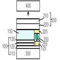
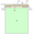
도 1은 본 발명의 플렉서블 유기 발광 표시 장치의 제조 공정을 나타낸 공정 순서도이며, 도 2a 내지 도 2d는 본 발명의 플렉서블 유기 발광 표시 장치의 제조 공정을 나타낸 공정 단면도이다. 그리고, 도 3은 제 2 글래스 기판 제거 후 단위 패널별 스크라이빙을 나타낸 사시도이고, 도 4는 도 3의 스크라이빙 단위 패널의 제 2 기재 컷팅을 나타낸 평면도이다.FIG. 1 is a flow chart showing a manufacturing process of a flexible organic light emitting display according to the present invention, and FIGS. 2 (a) to 2 (d) are process sectional views showing a manufacturing process of a flexible organic light emitting display according to the present invention. FIG. 3 is a perspective view showing scribing for each unit panel after the removal of the second glass substrate, and FIG. 4 is a plan view showing a second substrate cutting of the scribing unit panel of FIG.
도 1 내지 도 4와 같이, 본 발명의 플렉서블 유기 발광 표시 장치는 다음의 순서로 제조 공정이 이루어진다.As shown in FIGS. 1 to 4, the flexible organic light emitting display of the present invention is manufactured in the following order.
먼저, 도 2a와 같이, 제 1 글래스 기판(300) 상에, 제 1 플렉서블 기재(110)를 형성하고, 상기 제 1 플렉서블 기재(110) 상에, 차례로, 박막 트랜지스터 어레이(120)와 유기 발광 다이오드 어레이(130)를 형성한다(100S). 여기서, 상기 박막 트랜지스터 어레이(120)와 유기 발광 다이오드 어레이(130)는 제 1 플렉서블 기재(110)의 액티브 영역에 위치하며, 같은 기재 상에 위치한 두 어레이(120, 130)를 포함하여 하부 어레이(박막 트랜지스터 및 유기 발광 다이오드 어레이 포함)(100)라 한다.First, as shown in FIG. 2A, a first
또한, 상기 박막 트랜지스터 어레이(120)를 형성하는 동일 공정에서, 액티브 영역 외측 패드부에 박막 트랜지스터 어레이 패드 전극(135) 및 더미 패드 전극(125)을 형성한다.In addition, in the same step of forming the thin
한편, 상기 박막 트랜지스터 어레이(120) 형성시 상기 액티브 영역 외곽의 패드부에, 상기 박막 트랜지스터 어레이(120)와 전기적으로 연결되는 어레이 패드 전극(135)이 구비되고, 또한, 상기 어레이 패드 전극(135)과 이격하며, 패드부의 양단에 대응되어 더미 패드 전극(125)이 구비된다. An
또한, 상기 박막 트랜지스터 어레이(120) 또는 상기 유기 발광 다이오드 어레이(130) 형성시 상기 액티브 영역 외곽에 어레이 패드 전극(135)이나 더미 패드 전극(125)과 이격되는 점등 검사 패턴(145)이 더 구비될 수 있다. 이는 일종의 테스트 패턴으로 경우에 따라 생략되거나 위치를 달리할 수 있다.Further, when the thin
이어, 상기 도 2b와 같이, 제 2 글래스 기판(400) 상에, 제 2 플렉서블 기재(210)를 구비한 후, 그 상부에 터치 센싱 어레이(210)를 구성한다(110S). 여기서, 상기 제 2 플렉서블 기재(210)와 터치 센싱 어레이(210)를 포함하여 상부 어레이(200)라 한다.2B, a second
이어, 상기 제 2 글래스 기판(400)의 액티브 영역에 접착층(150)을 도포한다.Next, the
그리고, 이러한 상기 센싱 어레이(210) 형성시에도, 동일 공정에서, 상기 더미 패드 전극(125)과 대응되는 위치에, 터치 패드 전극들(225)이 형성된다. 또한, 상기 접착층(150)과 이격하며, 상기 터치 패드 전극들(225) 상에 도전 볼(255)을 포함한 이방성 도전 필름(250)을 도포한다.Also, when the
한편, 상기 도 2a의 박막 트랜지스터 어레이(120)와 유기 발광 다이오드 어레이(130)이나 도 2b의 터치 센싱 어레이(210)의 형성은 그 순서로 반대로 하여도 좋다. 또한, 상기 박막 트랜지스터 어레이(120)와 유기 발광 다이오드 어레이(130)이나 도 2b의 터치 센싱 어레이(210)가 형성되는 부위는 제 1 플렉서블 기재(110)과 제 2 플렉서블 기재(120)의 액티브 영역에 해당되며, 액티브 영역의 외곽에는 패드부가 정의된다.The
상기 제 1 글래스 기판(300)과 제 2 글래스 기판(400)은 각각 원장 상태에서 어레이들을 형성하는 것으로, 각 글래스 기판(300, 400)은 복수개의 패널들이 단위 패널로 나뉘지 않은 상태로, 영역을 달리하여 개별 어레이 공정이 진행된다. 즉, 도 3에서 도시된 바와 같이, 제 1 글래스 기판(300)이나 제 2 글래스 기판(400)은 수평적으로 복수개의 패널들의 어레이들이 구비된다.The
이어, 도 2c와 같이, 하부 어레이(100)와 상부 어레이(200)가 각각의 어레이 형성면이 서로 마주보도록 상기 제 2 글래스 기판(400)을 반전시켜, 상기 접착층(150)을 통해, 마주본 어레이들(130, 210)이 합착되도록 한다(120S). 이 과정에서, 상기 제 1, 제 2 글래스 기판(300, 400)의 상하 방향으로 압력을 가하여, 평면에 균등히 힘이 제공되며, 합착이 이루어진다. 상기 접착층(150)을 통한 어레이들의 합착시 동일한 압력에 의해, 상기 더미 패드 전극(125)와 상기 터치 패드 전극(225)간에 이방성 도전 필름(250) 내에 있는 상기 도전성 볼(255)이 깨지며, 두 전극(125, 225)의 전기적 도통을 이루게 된다.Next, as shown in FIG. 2C, the
이어, 도 2d와 같이, 합착되어 있는 제 1, 제 2 글래스 기판(300, 400) 중 상측에 위치한 제 2 글래스 기판(400)에 레이저를 조사하여, 상기 제 2 플렉서블 기재(210)로부터 상기 제 2 글래스 기판(400)이 탈리(脫離)되도록 한다(130S).2d, a laser beam is irradiated onto the
이어, 도 3과 같이, 제 2 글래스 기판(400)이 탈리되어 오픈된 제 2 플렉서블 기재(210)의 배면측에서 레이저를 조사하여 단위 패널별로 스크라이빙한다(140S). 이러한 스크라이빙된 라인을 기준으로 나뉜 단위 패널에서는 하측의 제 1 글래스 기판(300)은 유지된 상태로, 이는 상기 패드부에서 플렉서블 인쇄회로기판(FPCB) 등과 본딩이 이루어질 때, 가해지는 압력이나 열에 대해 내성을 갖기 위함이다.Next, as shown in FIG. 3, a laser beam is irradiated from the back side of the second
한편, 스크라이빙된 단위 패널에 대해 도 4와 같이, 패드부에 대응되는 상기 제 2 플렉서블 기재(210)의 일부를 컷팅한다(150S). 이러한 컷팅을 완료 후에는, 상대적으로 상기 제 1 플렉서블 기재(110)는 상기 제 2 플렉서블 기재(210)보다 돌출된 상태이며, 돌출된 부위에 상기 점등 검사 패턴(145)과 어레이 패드 전극(135)이 노출된다. 또한, 이러한 컷팅에서도 상기 터치 패드부에 대해서는 상기 더미 패드 전극(125)과 상기 터치 패드 전극(225)이 서로 전기적 접속을 이룬 상태를 유지하도록, 상기 제 2 플렉서블 기재(210)가 상기 제 1 플렉서블 기재(110)를 중첩한 상태를 유지한다.On the other hand, for the scribed unit panel, as shown in FIG. 4, a part of the second
상기 제 2 플렉서블 기재(210)의 컷팅은 대략적으로, 패드부가 위치한 제 1 플렉서블 기재(110)의 제 1 변의 에지가 노출되며 상기 더미 패드 전극(125)은 가리도록, 상기 패드부의 양단에 대해서는 나오고, 상기 패드부 양단 사이에는 들어가도록 하여 상기 액티브 영역(AA)에 보다 인접하게 하여, 이루어진다. 즉, 상기 제 2 플렉서블 기재(210)는 패드부에서만 상기 제 1 플렉서블 기재(110) 대비 컷팅되어 있는 것으로, 액티브 영역 및 그 주변에서는 상기 제 1 플렉서블 기재(110)의 중첩을 유지한다. 그리고, 컷팅된 상기 제 2 플렉서블 기재(210)로부터 점등 검사 패턴(135) 및 어레이 패드 전극(145)이 노출되게 되며, 패드부에서 상기 제 1 플렉서블 기재(110)와 제 2 플렉서블 기재(210)간의 영역 차를 갖게 된다.The cutting of the second
여기서, 상기 제 1 플렉서블 기재(110) 및 제 2 플렉서블 기재(120)는 각각 투명한 플라스틱 필름이거나 혹은 복수층의 무기막이거나 혹은 이들은 모두 포함한 형태일 수 있다. 상기 제 1, 제 2 플렉서블 기재(110, 120)는 각각 20㎛ 이내의 두께로, 상기 제 1, 제 2 글래스 기판(300, 400)의 두께 대비 1/20 이하로, 충분히 얇고 유연성을 가져, 이의 합착으로 제조된 플렉서블 유기 발광 표시 장치가 접히거나 말릴 수 있는 상태를 유지하게 된다. Here, the first
이어, 상기 어레이 패드 전극들(145) 상에, 어레이 및 터치 패드 전극으로 신호를 전달할 수 있는 플렉서블 인쇄 회로 기판(미도시)을 접속한다(160S).Next, a flexible printed circuit board (not shown) capable of transmitting signals to the array and touch pad electrodes is connected to the array pad electrodes 145 (160S).
이어, 상기 제 1 글래스 기판(300)을 제거하여(170S), 상기 제 1 플렉서블 기재(110)를 노출시킨다.Next, the
경우에 따라, 상기 노출된 제 1 플렉서블 기재(110) 하측은 베젤에 수납을 위해 상대적으로 제 1 플렉서블 기재(110) 대비 강성을 유지하도록 두께를 더 갖는 백 커버 필름이 더 부가될 수 있다.In some cases, the exposed first
상술한 설명에서 상기 제 1, 제 2 플렉서블 기재(110, 210)는 각각 유연성을 갖는 내열성 투명 플라스틱 필름과, 투명 플라스틱 필름으로, 그 성분은 폴리에스테르(polyester) 또는 폴리 에스테르를 포함하는 공중합체, 폴리이미드(polyimide) 또는 폴리 이미드를 포함하는 공중합체, 올레핀계 공중합체, 폴리아크릴산(polyacrylic acid) 또는 폴리아크릴산을 포함하는 공중합체, 폴리스티렌(polystyrene) 또는 폴리스테린을 포함하는 공중합체, 폴리설페이트(polysulfate) 또는 폴리설페이트를 포함하는 공중합체, 폴리카보네이트(polycarbonate) 또는 폴리 카보네이트를 포함하는 공중합체, 폴리아믹산(polyamic acid) 또는 폴리아믹산을 포함하는 공중합체, 폴리아민(polyamine) 및 폴리아믹산을 포함하는 공중합체, 폴리비닐 알콜(polyvinylalcohol), 폴리 알릴아민(polyallyamine)으로 이루어진 군에서 선택되는 하나 이상의 고분자 화합물을 포함할 수 있으며, 그 두께는, 상기 플라스틱 필름의 두께는 5㎛ 내지 100㎛일 수 있다. 경우에 따라, 상기 제 2 플렉서블 기재(210)는 투명 무기막만 구비될 수 있다. 이 경우, 투명 무기막은 복수층일 수 있으며, 그 성분으로는 질화막, 산화막, 산화질화막 혹은 금속 산화막일 수 있다. In the above description, the first and second
한편, 본 발명의 플렉서블 유기 발광 표시 장치에 있어서는 상기 제 2 글래스 기판(400) 제거 공정에서, 레이저 조사 외에 상기 제 2 글래스 기판(400)을 들어올리는 외력이 가해지는데, 이러한 과정에서, 실험상 제 2 플렉서블 기재(210)의 가장 얇은 부분인 터치 라우팅 배선의 부위에서, 크랙이 발생됨을 주목하여, 상기 터치 라우팅 배선의 위치를 변경하고자 한다.Meanwhile, in the flexible organic light emitting display device of the present invention, in the process of removing the
즉, 터치 라우팅 배선(도 5의 227 참조)이 패드부에서 접착층(150)이나 이방성 도전 필름(250)과 중첩되지 않은 부위에서, 크랙이 발생됨을 고려하여, 터치 라우팅 배선(227)의 위치를, 터치 센싱 어레이(220)에서 수직 방향의 측부를 따라 진행하여, 상기 터치 패드부로 들어오도록 한다. That is, in consideration of the occurrence of a crack at a portion where the touch routing wiring (see 227 in FIG. 5) does not overlap the
한편, 도 4를 참조하면, 단위 패널이 대략 직사각형의 형상일 때, 상기 단위 패널에서, 4변 중 일변을 따라 패드부가 정의되며, 상기 패드부와 인접하여 직사각형의 액티브 영역(AA)이 정의된다. 상대적으로 패드부가 있는 변의 에지가 다른 변들의 에지에 비해, 상기 액티브 영역으로부터 멀리 떨어져 있으며, 상기 패드부가 있는 변이 상기 액티브 영역(AA)과 이격한 간격은 상기 패드부의 폭에 상당하다.4, when a unit panel has a substantially rectangular shape, a pad portion is defined along one side of four sides in the unit panel, and a rectangular active region AA is defined adjacent to the pad portion . The edge of the side having the pad portion relatively is distant from the active region as compared with the edge of the other sides and the interval where the side having the pad portion is separated from the active region AA corresponds to the width of the pad portion.
이를 도 4 및 도 5를 참조하여 설명한다.This will be described with reference to FIGS. 4 and 5. FIG.
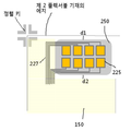
도 5은 본 발명의 제 1 실시예에 따라 도 4의 좌측 터치 패드부를 확대한 평면도이다.5 is an enlarged plan view of the left touch pad unit of FIG. 4 according to the first embodiment of the present invention.
한편, 도 2a 내지 도 4와 같이, 일반적인 플렉서블 유기 발광 표시 장치에서 공통적으로 갖는 직사각형이며, 제 1 변을 따라 일정 폭의 패드부를 가지며, 상기 패드부와 인접하며 나머지 3변의 가장자리로부터 소정 간격 이격하여 액티브 영역을 갖는 제 1 플렉서블 기재(110)와, 상기 제 1 플렉서블 기재의 액티브 영역 상에 구비된 박막 트랜지스터 및 유기 발광 다이오드 어레이(120, 130)와, 상기 액티브 영역과 상기 제 1 변을 따른 패드부의 양단과 중첩된 제 2 플렉서블 기재(210)와, 상기 제 2 플렉서블 기재 상에, 상기 제 1 플렉서블 기재의 액티브 영역을 마주보며 구비된 터치 센싱 어레이(220)의 설명은 이하에서 생략한다.As shown in FIGS. 2A to 4, a common flexible organic light emitting display device has a pad portion having a predetermined width along the first side, adjacent to the pad portion, and spaced apart from the edges of the remaining three sides A thin film transistor and an organic light emitting diode array (120, 130) provided on an active region of the first flexible substrate; a plurality of pads The second
도 4 및 도 5와 같이, 본 발명의 제 1 실시예에 따른 플렉서블 유기 발광 표시 장치의 상하 본딩 관점에서 그 구성을 살펴보면, 상기 제 2 플렉서블 기재 상에, 상기 패드부의 양단과 중첩된 부위에 구비된 복수개의 터치 패드 전극(225)을 포함하는 터치 패드부와, 상기 터치 패드부와 상기 패드부 양단의 층간에 위치한 도전성 볼(255)을 갖는 이방성 도전 필름(250)과, 상기 박막 트랜지스터 및 유기 발광 다이오드 어레이(120, 130)와 상기 터치 센싱 어레이(220) 사이의 층간에 위치하며, 상기 제 1 변과 수직한 방향에서, 상기 이방성 도전 필름(250)과 접한 접착층(150) 및 상기 제 2 플렉서블 기재(210) 상의 상기 액티브 영역의 외곽에서 상기 접착층(150)과 중첩하며, 상기 터치 센싱 어레이(220)와 접속되어, 상기 복수개의 터치 패드 전극(225)과 연결된 복수개의 터치 라우팅 배선(227)을 포함한다. As shown in FIGS. 4 and 5, the flexible organic light emitting display according to the first embodiment of the present invention has a structure in which the first and second flexible substrates are overlapped with both ends of the pad unit. An anisotropic
도 5와 같이, 본 발명의 제 1 실시예에 따른 플렉서블 유기 발광 표시 장치는 상기 터치 패드부에서, 상기 터치 패드 전극들(225)은 상기 제 1 변을 따라 2행으로 정렬되며, 2행의 터치 패드 전극들(225)은 상기 제 1 변과 교차하는 방향에서 서로 연결되고, 연결된 2개의 터치 패드 전극들(225)이 각각 상기 터치 라우팅 배선들(227)과 연결되어 있다.5, in the flexible organic light emitting display according to the first embodiment of the present invention, in the touch pad unit, the
특히, 본 발명의 플렉서블 유기 발광 표시 장치에 있어서, 터치 라우팅 배선들(227)은 수평 방향에서 발생하는 접착층(150)과 이방성 도전 필름(250)간의 이격 공간이 있더라도, 수직한 측부에 이방성 도전 필름(250)과 접하는 접착층(150)과 중첩하도록 위치시켜, 터치 라우팅 배선들(227)이 제 2 플렉서블 기재(210) 표면에 갖는 접착력을 높이고 보호를 꾀한 것이다. 이를 통해 터치 라우팅 배선들(227)의 크랙을 방지하고, 터치 채널 오픈을 방지하여 장치 전체의 수율을 향상시킬 수 있다.Particularly, in the flexible organic light emitting display according to the present invention, even if there is a space between the
한편, 상기 이방성 도전 필름(250)은 상기 제 2 플렉서블 기재(210)의 제 1 변(도시된 도 5의 정렬 키의 중앙을 지나는 수평라인) 방향의 에지로부터 제 1 간격(d1)이 이격된 것이 바람직하다. 이는 제 2 플렉서블 기재(210)를 제 2 글래스 기판(400) 제거 후 컷팅시 이방성 도전 필름(250)이 컷팅 라인에 남아있는 경우, 컷팅이 정상적으로 이루어지지 않기 때문에, 상기 제 2 플렉서블 기재(210)의 에지를 피하여, 에지 안쪽으로 이방성 도전 필름(250)이 도포되어야 하기 때문이다.On the other hand, the anisotropic
또한, 상기 이방성 도전 필름(250)은 상기 제 1 변을 따른 방향에서 상기 접착층(150)과 제 2 간격(d2) 이격된다. 이 경우, 수평 방향에서 접착층(150)과 상기 이방성 도전 필름(250)간의 중첩을 방지하여, 본딩 과정에서 특정 부위가 들뜸을 방지한다. 또한, 수평 방향에서 상기 제 2 간격(d2)이 요구되는 이유는, 상대적으로 수직 방향의 측부에 비해 넓은 수평 방향의 영역에서 압력이 가해질 때, 접착층(150)이나 이방성 도전 필름(250)의 퍼짐 편차가 크기 때문에, 접착층(150)과 이방성 도전 필름(250)을 접하게 도포하거나 중첩 도포시, 압력이 가해지며, 접착층(150)과 이방성 도전 필름(250)간의 중첩이 심해져 해당 부위의 들뜸이 있기 때문이다. 이를 방지하기 위해, 본딩/프레스의 가압을 고려하여, 접착층(150)과 이방성 도전 필름(250)간 제 2 간격(d2)을 구비한 것이다. 이 경우, 압력이 가해져도 상기 접착층(150)의 수평 방향에서는 상기 이방성 도전 필름(250)이 접착층(150)과 접하지 않아, 본딩 들뜸을 방지할 수 있고, 또한, 상기 제 2 간격(d2)에는 터치 라우팅 배선(227)이 위치하지 않아, 터치 라우팅 배선(227)이 접착층(150)과 비중첩되는 영역을 생성하지 않아 제 2 글래스 기판(400) 제거 후에도 터치 라우팅 배선(227)이 크랙되는 현상을 방지할 수 있다.Also, the anisotropic
여기서, 상대적으로, 패드부의 길이 방향과 교차하는 상기 제 1 변과 수직한 방향의 터치 패드부의 측부에서, 접착층(150)과 이방성 도전 필름(250)의 인접하게 도포한 경우, 수직 방향의 터치 패드부가 짧기 때문에, 압력이 가해질 때, 압력에 의해 퍼지는 접착층(150)과 이방성 도전 필름(250)은 서로 중첩하지 않고, 상하 방향으로 퍼져 접착층(150)과 이방성 도전 필름(250)이 경계부에서 서로 그 영역을 달리하고, 따라서, 터치 패드부의 수직 측부(제 1 변에 수직한 방향)에 위치한 터치 라우팅 배선(227)이 접착층(150)과 오버랩되어 특정 부위의 배선 노출을 배제하여 배선 크랙을 방지할 수 있는 것이다. Here, when the
이와 같이, 수평 방향의 영역들(제 1 변을 따른 방향)에서 접착층(150)이나 이방성 도전 필름(250)이 구비되지 않은 영역(제 1 간격 및 제 2 간격)이 존재하나, 이는 대략 10㎛~400㎛의 간격이며, 상대적으로 제 2 간격(d2)이 제 1 간격(d1)에 비해 작을 수 있다. As described above, regions (the first gap and the second gap) in which the
한편, 상기 접착층(150)과 이방성 도전 필름(250)은 서로 재질이 달라 제 1, 제 2 글래스 기판(300, 400)을 합착하는 과정에서, 동일한 평면적 압력이 인가되어도 다른 신장성을 갖는다. 또한, 국부적인 영역에 한정되는 이방성 도전 필름(250)에 비해 액티브 영역을 포함하여 터치 패드부를 제외한 영역들까지 구비되는 접착층(150)이 보다 늘어나는 면적이 크다. 예를 들어, 접착층(150)은 두께가 10㎛인 경우, 최대 381.6㎛ 늘어나며, 평균 200㎛ 늘어난다. 또한, 두께가 15 ㎛인 경우, 최대 445.7㎛ 늘어나며, 평균 250㎛ 늘어난다. 즉, 접착층(150)은 두께에 따라 비례하므로, 접착층(150) 및 이방성 도전 필름(250)의 신장률 및 재료 등을 고려하여, 상기 제 1 간격(d1) 및 제 2 간격(d2)을 조절한다.The
또한, 상기 터치 라우팅 배선(227)은 수직 방향(제 1 방향과 교차하는 방향)으로 위치하기 때문에, 상기 터치 패드부와 수평 방향으로 위치하는 접착층의 끝 사이의 제 2 간격(d2)에 위치하지 않아, 상기 제 2 간격(d2)과 비중첩될 수 있다.In addition, since the
또한, 상기 제 2 플렉서블 기재(210)로부터 노출된 상기 패드부에 상기 박막 트랜지스터 및 유기 발광 다이오드 어레이(120, 130)와 연결된 어레이 패드 전극(145)를 구비할 수 있다. The pad portion exposed from the second
그리고, 상기 터치 패드 전극들(225)과 대응되어, 상기 제 1 플렉서블 기재 (110) 상에, 더미 패드 전극들(125)이 구비되고, 그 사이에 층간에 위치하는 이방성 도전 필름(250) 내의 도전성 볼(255)이 압력에 의해 깨지며, 더미 패드 전극(125)과 터치 패드 전극(225)간의 접속이 이루어지는 것이다.The
이 경우, 본 발명의 제 1 실시예에 있어서는, 상기 터치 패드 전극(225)이 2개씩 연결되어, 하나의 더미 패드 전극(125)과 연결될 수 있으며, 실제 터치 관련 구동 신호는 제 1 플렉서블 기재(110) 상에, 상기 어레이 패드 전극(145)이 위치한 패드부와 배선을 통해 상기 더미 패드 전극(125)과 평면상으로 연결(미도시)시켜 이루어질 수 있다.In this case, in the first embodiment of the present invention, the two
도 6은 본 발명의 제 2 실시예에 따라 도 4의 좌측 터치 패드부를 확대한 평면도이다.6 is an enlarged plan view of the left touch pad unit of FIG. 4 according to the second embodiment of the present invention.
도 6과 같이, 상술한 제 1 실시예와 다른 예로, 본 발명의 제 2 실시예에 따른 유기 발광 표시 장치는, 상기 터치 라우팅 배선들(227)은 상기 터치 패드 전극들(225)과 각각 연결된 형상을 나타낸 것으로, 터치 라우팅 배선(227)과 터치 패드 전극(225)은 일대일 관계로 접속되어 있다.6, the organic light emitting display according to the second embodiment of the present invention is different from the first embodiment in that the
이러한 제 1 실시예와 제 2 실시예는, 상기 터치 패드 전극(225)과 터치 라우팅 배선(227)간의 연결 관계가 2:1인지, 1:1인지에만 차이가 있으며, 나머지 구성은 동일하며, 동일 기능을 한다. The first embodiment and the second embodiment differ only in whether the connection relation between the
또한, 이 경우에도 상기 터치 라우팅 배선(227)은 터치 패드부의 수직 측부(제 1 변의 방향과 수직한 방향)에 위치한다.Also in this case, the
한편, 도 6에 도시된 터치 패드 전극(225)은 8개 구비된 예를 나타내었으나, 이에 한하지 않으며, 터치 센싱 어레이(220)에 구비되어 신호 인가가 필요한 터치 전극의 수에 따라 변화할 수 있다. 또한, 터치 패드 전극(225)의 수가 늘 경우, 터치 라우팅 배선(227)의 수도 늘게 되는데, 어느 경우나 터치 라우팅 배선(227)은 터치 패드부 측부에서, 상기 접착층(15)과 중첩 관계를 유지하여, 외력에 대해 상기 터치 라우팅 배선(227)이 받는 스트레스를 방지할 수 있다.6, the number of the
도 7a 및 도 7b는 비교예와 본 발명의 제 1 실시예의 접착층과 라우팅 배선과의 대응 관계를 나타낸 평면도이다.7A and 7B are plan views showing a correspondence relationship between the adhesive layer and the routing wiring in the comparative example and the first embodiment of the present invention.
도 7a와 같이, 비교예에 있어서는, 터치 센싱 어레이로부터 나온 터치 라우팅 배선(27)이 이방성 도전 필름(25)의 하측부를 지나도록 구비되어 있다. 이 경우, 터치 라우팅 배선(27)은 이방성 도전 필름(25)과 접착층(15) 사이의 이격 공간을 지나게 되어, 이격 공간 상의 상기 터치 라우팅 배선(27)이 제 2 글래스 기판 제거시 취약하여, 이 부위에서 배선 크랙이 발생하는 문제가 있다. 즉, 상부의 제 2 플렉서블 기재 상의 터치 패드 전극(30)과 하부의 제 1 플렉서블 기재 상의 더미 패드 전극(미도시)을 전기적으로 연결하는 콘택 영역이 존재하게 되는데, 제 2 글래스 기판 제거시 접착층(15)과 이방성 도전 필름(25) 사이의 빈 공간이 발생하게 되면, 빈 공간에 대응된 터치 라우팅 배선이 상부 글래스 제거시 스트레스에 취약하여, 배선 크랙이 발생할 수 있는 것이다.As shown in FIG. 7A, in the comparative example, the
도 7b와 같이, 본 발명의 제 1 실시예에 있어서는, 이와 같은 문제를 해결하고자 이방성 도전 필름(250)과 접착층(150) 사이의 제 2 이격 공간을 터치 라우팅 배선을 지나지 않도록, 이방성 도전 필름(250)의 측부를 통해 상기 터치 라우팅 배선(227)이 상기 터치 패드 전극(225)과 만나도록 하여, 터치 라우팅 배선(227) 전체가 접착층(15) 혹은 이방성 도전 필름(250)과 중첩하도록 하여, 비교예의 문제를 해결할 수 있다.7B, in order to solve such a problem, in the first embodiment of the present invention, a second spacing space between the anisotropic
즉, 터치 센싱 어레이(220)의 각 제 1, 제 2 터치 전극(221, 223)에 연결되는 터치 라우팅 배선(227) 위치 및 접착층(150)의 타발 위치 변경을 통하여 접착층(150)과 이방성 도전 필름(250) 사이의 빈공간이 발생하여도 제 2 글래스 기판(400) 제거(releasing)시 스트레스에 의한 터치 채널 오픈 불량을 개선할 수 있다. That is, the position of the
한편, 평면적으로 상기 이방성 도전 필름(250) 위쪽에는 상기 제 2 플렉서블 기재(210)를 커팅하는 레이저 커팅 라인이 위치하고, 하부쪽은 접착층(150)이 위치하고 있어 이방성 도전 필름(250)의 (평면상) 상하로 늘어남에 제어가 불가한 반면, 좌우 영역은 레이저 커팅이나 액티브 영역이 바로 접하여 있지 않아, 그 폭 제어가 용이하며, 따라서, 터치 라우팅 배선(227)의 구비가 가능한 것이다. On the other hand, a laser cutting line for cutting the second
한편, 하기 표 1은 비교예와 본 발명의 제 1 실시예에 대해서는 3차에 거쳐 터치 라우팅 배선의 오픈 불량을 검사하였다.On the other hand, in Table 1, open failure of the touch routing wiring was checked through the third example for the comparative example and the first embodiment of the present invention.
즉, 비교예의 경우는, 터치 라우팅 배선들의 불량이 34%, 40%, 37%로 모두 34% 이상의 불량이 나타났고, 반면, 본 발명의 제 1 실시예의 경우는 2%, 3%, 1%로, 모두 3% 이하의 불량이 나타났다. 따라서, 5% 이하의 불량을 터치 센싱에 영향을 주지 않을 정도로, 본 발명의 제 1 실시예 적용시 배선 크랙이나 터치 채널의 오픈 문제를 해결할 수 있음을 알 수 있다.That is, in the case of the comparative example, the defects of the touch routing wirings were 34%, 40%, and 37%, respectively, which were more than 34% , All of which showed defects of less than 3%. Therefore, it can be seen that wiring cracks and the open problem of the touch channel can be solved when the first embodiment of the present invention is applied to such a degree that defective of 5% or less does not affect the touch sensing.
도 8은 도 7a의 비교예에서 나타나는 크랙을 나타낸 사진이다.FIG. 8 is a photograph showing a crack in the comparative example of FIG. 7A. FIG.
도 8의 사진을 살펴보면, 상기 이방성 도전 필름과 접착층 사이의 이격 공간에 위치한 터치 라우팅 배선에 크랙이 발생된 형상을 나타내고 있다. 즉, 비교예와 같이, 터치 센싱 어레이에서, 터치 패드부의 수평 방향의 배열된 터치 패드 전극에 바로 터치 라우팅 배선이 위치하는 경우, 이격 공간 내에서 어느 접착 재료에 의해서도 제 2 플렉서블 기재 상에 접착되지 않은 터치 라우팅 배선은 크랙이 발생함을 알 수 있다.8, a crack is generated in a touch routing wiring located in a space between the anisotropic conductive film and the adhesive layer. That is, as in the comparative example, in the case where the touch routing wiring is directly disposed on the touch pad electrodes arranged in the horizontal direction of the touch pad unit in the touch sensing array, the touch routing electrode is not bonded to the second flexible substrate by any adhesive material It can be seen that the non-touch routing wiring is cracked.
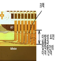
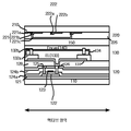
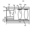
도 9a 내지 도 9c는 본 발명의 플렉서블 유기 발광 표시 장치의 액티브 영역과, 도 5의 I~I' 선상 및 Ⅱ~Ⅱ' 선상을 자른 단면도이다.FIGS. 9A to 9C are cross-sectional views of the active region of the flexible organic light emitting display device of the present invention, taken along lines I to I 'and II to II' of FIG. 5, respectively.
도 9a 내지 도 9c와 같이, 본 발명의 플렉서블 유기 발광 표시 장치는, 제 1 플렉서블 기재(110) 상에, 상기 박막 트랜지스터 어레이(120), 유기 발광 다이오드 어레이(130)를 구비하고, 상기 제 2 플렉서블 기재(210) 상에 터치 센싱 어레이(220)을 구비하고, 각 어레이의 동일 대응 위치에 액티브 영역(AA)과 외곽 영역을 구비한다. 그리고, 액티브 영역에는 평면적으로, 복수의 화소를 매트릭스 상으로 구비하며, 각각 박막 트랜지스터 어레이(120)는 화소별로 나뉘는 서로 교차하는 게이트 라인 및 데이터 라인과, 화소별로 하나 이상의 박막 트랜지스터(TFT)를 구비하고, 유기 발광 다이오드 어레이(130)는 유기 발광 다이오드(OLED)를 구비한다. 상기 터치 전극 어레이(220)는 액티브 영역에 복수개의 서로 교차하는 제 1 터치 전극(221) 및 제 2 터치 전극(222)을 구비한다. 상기 제 1, 제 2 터치 전극(221, 222)의 배치는 복수의 화소에 대응할 수 있으나, 화소의 배열에 무관하게 배치될 수도 있다.9A to 9C, the flexible organic light emitting display device of the present invention includes the thin
또한, 박막 트랜지스터 어레이(120)의 외곽 영역에는 패드부가 구비되며, 상기 터치 전극 어레이(220)는 상기 박막 트랜지스터 어레이(120)의 패드부에 구비된 더미 패드 전극(125)과 접속되는 터치 패드부를 구비한다. 여기서, 상기 터치 패드부가 상기 박막 트랜지스터 어레이(120)의 패드부와 연결되는 이유는 터치 전극 어레이(220) 측에 별도의 FPC 연결을 피하고, 터치 제어를 위한 신호 인가를 박막 트랜지스터 어레이(120)와 동일면에 있는 패드부로부터 받기 위함이다. 이는 공정 단순화와 FPC 연결 최소를 위함이기도 하다.The
상기 박막 트랜지스터 어레이(120)의 화소 내 박막 트랜지스터(TFT)는, TFT 버퍼층(121) 상의 액티브층(122)과, 상기 액티브층(122)을 덮으며 TFT 버퍼층(121) 상에 형성된 게이트 절연막(124a)과, 상기 액티브층(122)과 중첩하는 게이트 전극(123)과, 상기 게이트 전극(123)과 상기 게이트 절연막(124a) 상에 형성된 층간 절연막(124b)과, 상기 층간 절연막(124b), 게이트 절연막(124a)을 관통하여 상기 액티브층(122)의 양단과 접속한 소오스 전극(125) 및 드레인 전극(126)을 포함한다. 여기서, 상기 게이트 전극(123)은 게이트 라인과 동일층에 위치할 수 있으며, 소오스 전극(125) 및 드레인 전극(126)은 상기 데이터 라인과 동일층에 위치할 수 있다.The thin film transistor (TFT) of the thin
상기 박막 트랜지스터 어레이의 외곽 영역에는 게이트 라인 및 데이터 라인용 패드 전극과 유기 발광 다이오드 어레이의 제 2 전극을 접지시키거나 혹은 일정한 전압을 인가하는 제 2 전극 패드 전극을 구비하며, 또한, 도시된 바와 같이, 상측의 이방성 도전 필름 (250) 내의 터치 패드 전극(225)과 접속되는 더미 전극 패드(125)을 구비할 수 있다.And a second electrode pad electrode for grounding or applying a predetermined voltage to the pad electrode for the gate line and the data line and the second electrode of the organic light emitting diode array is formed in an outer area of the thin film transistor array, And a
유기 발광 다이오드(OLED)는 상기 드레인 전극(116)과 접속되는 제 1 전극(131)과, 발광 영역을 정의하는 뱅크(132a) 내에 형성된 유기 발광층(133) 및 상기 유기 발광층(133)을 덮는 제 2 전극(134)을 포함한다. 여기서, 상기 유기 발광 다이오드(OLED)는 박막 트랜지스터(TFT)를 보호막(128)을 통해 덮으며, 보호막(126)의 일부에 콘택홀을 형성하여, 상기 드레인 전극(126)과 접속한다. 상기 드레인 전극(126)과는 상기 제 1 전극(131)이 접속된다.The organic light emitting diode OLED includes a
경우에 따라 상기 뱅크(132a) 상에 뱅크(132a)의 일부 폭에 대응하여 일정 높이의 스페이서(132b)가 구비될 수 있다. 상기 스페이서(132b)는 유기 발광층(133)의 형성시 소정의 개구부를 통해 유기물을 투과시키는 금속 마스크를 제 1 플렉서블 기재(110)의 상측에 대응하여 유기물 증착 공정을 진행하는데, 이 과정에서 금속 마스크 처짐이 있어, 뱅크(132a)가 무너지거나 발광 영역 내부에 영향을 주는 점을 방지하기 위해, 뱅크(132a) 상에 규칙적으로 스페이서(132b)를 더 구비하는 것이다. 한편, 상기 제 1 전극(131)은 반사 전극이며, 상기 제 2 전극(134)은 투명 전극으로, 외부광이 입사시 반사는, 유기 발광 다이오드(OLED)를 통과하여 상기 제 1 전극(131)에서 이루어지며, 반사시 투명한 제 2 전극(134)을 통광하여 광이 진행되게 된다.A
그리고, 상기 유기 발광 다이오드 어레이(130)와 상기 터치 센싱 어레이(220) 사이에는, 접착층(150)이 구비된다. An
상기 터치 센싱 어레이(220)는 액티브 영역에 서로 교차하는 복수개의 제 1, 제 2 터치 전극(221, 222)과, 상기 제 1, 제 2 터치 전극(221, 222)을 덮는 보호막(226)과, 상기 외곽 영역에 상기 제 1, 제 2 터치 전극들(221, 222)과 대응된 복수개의 터치 패드 전극(225) 및 상기 터치 패드 전극(225)에서 상기 제 1, 제 2 터치 전극들(221, 222)에서 신호를 전달하는 라우팅 배선(227)을 포함한다.The
도시된 예에서, 제 1, 제 2 터치 전극(221, 222)과, 상기 라우팅 배선(227) 및 터치 패드 전극(225)은 각각 하측에 금속 메쉬 패턴(221a, 222a, 227a, 225a)을 구비하고, 상측에 투명 전극(221b, 222b, 227b, 225b)를 구비한 이층형 전극 구조이며, 이를 통해 전계 안정화와 저저항를 꾀한다. 그런데, 본 발명의 유기 발광 표시 장치에 있어서, 상기 터치 전극 어레이는 이러한 금속 메쉬 패턴을 포함하는 전극 구조에 한할 필요는 없고, 한 층의 전극 구조로도 구현 가능하다.In the illustrated example, the first and
또한, 제 1 터치 전극(221)과 제 2 터치 전극(222)은 도시된 예에서, 동일 표면에 위치하기에, 둘 간의 쇼트를 방지하기 위해, 제 1 전극(221)은 보호막(226) 내 구비된 콘택홀을 통해 브리지 패턴(221c)을 두어, 교차하는 제 2 전극(222)과 전기적으로 절연되도록 한다. The first electrode 221 and the
도시된 바와 같이, 제 1, 제 2 터치 전극(221, 222)과, 상기 라우팅 배선(227) 및 터치 패드 전극(225)은 상기 제 2 플렉서블 기재(210) 상에 위치한다. 또한, 제 2 플렉서블 기재(210)는 폴리 이미드와 같은 유기막의 단일 기재이거나 유기막과 복수층의 무기막의 적층 기재로 하며, 복수층의 무기막 최상단을 상기 터치 센싱 어레이(220)의 형성면으로 하거나, 혹은 폴리 이미드와 같은 유기막의 재료를 생략하여 복수층의 무기막만을 포함할 수도 있다. 어느 경우나, 상기 제 2 플렉서블 기재(210)은 투명한 기재로, 제 2 플렉서블 기재(210) 측이 표시면으로 이용되기 때문이다.The first and
또한, 도 9b와 같이, 터치 패드부에 대해, 터치 패드부의 수직한 측부에 대해서는 접착층(150)을 이방성 도전 필름(250)과 접하게 하며, 상기 터치 패드부의 수직한 측부에 위치하도록 터치 라우팅 배선(227)을 구비하여, 터치 라우팅 배선(227)은 그 상부 전체가 접착층(150)이 덮도록 하여, 터치 라우팅 배선(227)의 제 2 플렉서블 기재(210)에 대해 접착력을 강화시킨다. 이로써, 배선 크랙을 방지할 수 있다.9B, the
도 9c와 같이, 터치 패드부의 수평한 방향을 따른 하측부에 대해서, 터치 패드부의 이방성 도전 필름(250)이 제 2 이격 간격(d2)으로 이격하여 접착층(150)이 구비되어도, 상기 제 2 이격 간격 내에 터치 라우팅 배선(227)이 구비되지 않아, 터치 센싱 어레이의 터치 채널 크랙을 방지하여 수율 향상을 꾀할 수 있다.The anisotropic
한편, 도 9b 및 도 9c에 도시된 터치 라우팅 배선(227) 및 터치 패드 전극(225)은 이중층으로 도시되었으나, 이에 한하지 않으며, 단일층 혹은 삼중층으로 이루어질 수도 있다.Meanwhile, although the
본 발명의 플렉서블 유기 발광 표시 장치는, 인셀 터치(In-Cell type Touch) 유기 발광 패널 제작시, 터치 패드부의 콘택 신뢰성을 확보할 수 있는 것으로, 이방성 도전 필름 내의 터치 패드 전극과 연결되는 외측의 터치 라우팅 배선의 위치를 터치 패드부의 수직한 측부측에 있게 하여, 터치 라우팅 배선의 단선을 감소시키고, 불량률을 최소화할 수 있다. The flexible organic light emitting display device of the present invention can secure the contact reliability of the touch pad portion when manufacturing an organic light emitting panel of an in-cell type touch, The position of the routing wiring is located on the side of the vertical side of the touch pad portion, so that disconnection of the touch routing wiring can be reduced and the defect rate can be minimized.
인셀 터치 유기 발광 패널은 상부 터치 스크린 기판과 하부 박막 트랜지스터 기판을 합착하는 구조로 이루어진다. 이 때, 상부 터치 스크린 기판과 하부 박막 트랜지스터 기판을 전기적으로 연결하는 콘택 영역이 존재하게 되는데 상부 글래스 제거시 접착층과 도전성 접착 부재 사이의 빈 공간이 발생하게 되면 상부 글래스 제거 스트레스에 의한 배선 크랙이 발생한다.The Insel-touch organic luminescent panel has a structure in which an upper touch screen substrate and a lower TFT substrate are bonded together. At this time, a contact area for electrically connecting the upper touch screen substrate and the lower TFT substrate is present. When a space is formed between the adhesive layer and the conductive adhesive member during the removal of the upper glass, a wiring crack occurs due to the stress of removing the upper glass do.
본 발명은 이와 같은 문제를 해결하고자 터치 스크린 채널 전극에 연결되는 배선 위치 및 접착층 타발 위치 변경을 통하여 접착층과 도전성 접착 부재 사이의 빈공간이 발생하여도 상부 글래스 제거시 스트레스에 의한 터치 채널 오픈 불량을 개선하여 이로 인해 제품의 신뢰성 향상 및 불량률을 감소시킬 수 있다.In order to solve such a problem, the present invention has been made to solve the above problem by changing the wiring position and the adhesive layer punching position connected to the touch screen channel electrode, Thereby improving the reliability of the product and reducing the defect rate.
한편, 이상에서 설명한 본 발명은 상술한 실시예 및 첨부된 도면에 한정되는 것이 아니고, 본 발명의 기술적 사상을 벗어나지 않는 범위내에서 여러 가지 치환, 변형 및 변경이 가능하다는 것이 본 발명이 속하는 기술분야에서 통상의 지식을 가진 자에게 있어 명백할 것이다.While the present invention has been described in connection with what is presently considered to be the most practical and preferred embodiment, it is to be understood that the invention is not limited to the disclosed embodiments, but, on the contrary, is intended to cover various modifications and equivalent arrangements included within the spirit and scope of the appended claims. Will be apparent to those of ordinary skill in the art.
100: 하부 어레이 110: 제 1 플렉서블 기재
120: 박막 트랜지스터 어레이 125: 더미 패드 전극
130: 유기 발광 다이오드 어레이 135: 어레이 패드 전극
145: 점등 검사 패턴 150: 접착층
200: 상부 어레이 210: 제 2 플렉서블 기재
220: 터치 센싱 어레이 225: 터치 패드 전극
227: 터치 라우팅 배선 250: 이방성 도전 필름
255: 도전성 볼 300: 제 1 글래스 기판
400: 제 2 글래스 기판100: lower array 110: first flexible substrate
120: thin film transistor array 125: dummy pad electrode
130: organic light emitting diode array 135: array pad electrode
145: ON test pattern 150: Adhesive layer
200: upper array 210: second flexible substrate
220: touch sensing array 225: touch pad electrode
227: Touch routing wiring 250: Anisotropic conductive film
255: conductive ball 300: first glass substrate
400: second glass substrate
Claims (9)
상기 제 1 플렉서블 기재의 액티브 영역 상에 구비된 박막 트랜지스터 및 유기 발광 다이오드 어레이;
상기 액티브 영역과 상기 제 1 변을 따른 패드부의 양단과 중첩된 제 2 플렉서블 기재;
상기 제 2 플렉서블 기재 상에, 상기 제 1 플렉서블 기재의 액티브 영역을 마주보며 구비된 터치 센싱 어레이;
상기 제 2 플렉서블 기재 상에, 상기 패드부의 양단과 중첩된 부위에 구비된 복수개의 터치 패드 전극을 포함하는 터치 패드부;
상기 터치 패드부와 상기 패드부 양단의 층간에 위치한 이방성 도전 필름;
상기 박막 트랜지스터 및 유기 발광 다이오드 어레이와 상기 터치 센싱 어레이 사이의 층간에 위치하며, 상기 제 1 변과 수직한 방향의 터치 패드부의 측부에서, 상기 이방성 도전 필름과 접한 접착층; 및
상기 제 2 플렉서블 기재 상의 상기 액티브 영역의 외곽에서 상기 접착층과 중첩하며, 상기 터치 센싱 어레이와 접속되어, 상기 제 1 변과 수직한 방향의 터치 패드부의 측부에서, 상기 복수개의 터치 패드 전극과 연결된 복수개의 터치 라우팅 배선을 포함한 플렉서블 유기 발광 표시 장치.A first flexible substrate having a pad portion having a predetermined width along a first side and adjacent to the pad portion and having an active region spaced apart from edges of the remaining three sides by a predetermined distance;
A thin film transistor and an organic light emitting diode array provided on an active region of the first flexible substrate;
A second flexible substrate overlapping the active region and both ends of the pad portion along the first side;
A touch sensing array provided on the second flexible substrate so as to face the active area of the first flexible substrate;
A touch pad unit including a plurality of touch pad electrodes provided on a portion of the second flexible substrate overlapped with both ends of the pad unit;
An anisotropic conductive film disposed between the touch pad portion and a layer between both ends of the pad portion;
An adhesive layer disposed between the thin film transistor and the organic light emitting diode array and the touch sensing array and contacting the anisotropic conductive film at a side of a touch pad portion in a direction perpendicular to the first side; And
A plurality of touch electrodes connected to the plurality of touch pad electrodes, the plurality of touch pad electrodes being connected to the touch sensing array at a side of the touch pad unit in a direction perpendicular to the first side, overlapping the adhesive layer at an outer periphery of the active area on the second flexible substrate, Flexible organic light emitting display including touch routing wiring.
상기 이방성 도전 필름은 상기 제 1 변 방향에서, 상기 제 2 플렉서블 기재의 에지로부터 제 1 간격 이격된 플렉서블 유기 발광 표시 장치.The method according to claim 1,
Wherein the anisotropic conductive film is spaced apart from the edge of the second flexible substrate by a first interval in the first direction.
상기 이방성 도전 필름은 상기 제 1 변을 따른 방향에서 상기 접착층과 제 2 간격 이격된 플렉서블 유기 발광 표시 장치.3. The method of claim 2,
Wherein the anisotropic conductive film is spaced apart from the adhesive layer by a second interval in a direction along the first side.
상기 터치 라우팅 배선은 상기 제 2 간격과 비중첩된 플렉서블 유기 발광 표시 장치.The method of claim 3,
And the touch routing wiring is not overlapped with the second gap.
상기 제 2 플렉서블 기재는 상기 패드부의 양단 사이에서, 상기 액티브 영역에 인접하게 들어간 형상을 갖는 플렉서블 유기 발광 표시 장치.The method according to claim 1,
Wherein the second flexible substrate has a shape that is adjacent to the active region between both ends of the pad portion.
상기 제 2 플렉서블 기재로부터 노출된 상기 패드부에 상기 박막 트랜지스터 및 유기 발광 다이오드 어레이와 연결된 어레이 패드 전극을 구비한 플렉서블 유기 발광 표시 장치.6. The method of claim 5,
And an array pad electrode connected to the thin film transistor and the organic light emitting diode array in the pad portion exposed from the second flexible substrate.
상기 터치 패드 전극들과 대응되어, 상기 제 1 플렉서블 기재 상에, 더미 패드 전극들이 구비된 플렉서블 유기 발광 표시 장치.The method according to claim 1,
Wherein the dummy pad electrodes are provided on the first flexible substrate in correspondence with the touch pad electrodes.
상기 터치 라우팅 배선들은 상기 터치 패드 전극들과 각각 연결된 플렉서블 유기 발광 표시 장치.The method according to claim 1,
And the touch routing wires are connected to the touch pad electrodes.
상기 터치 패드부에서, 상기 터치 패드 전극들은 상기 제 1 변을 따라 2행으로 정렬되며, 2행의 터치 패드 전극들은 상기 제 1 변과 교차하는 방향에서 서로 연결되고, 연결된 2개의 터치 패드 전극들이 각각 상기 터치 라우팅 배선들과 연결된 플렉서블 유기 발광 표시 장치.The method according to claim 1,
In the touch pad portion, the touch pad electrodes are arranged in two rows along the first side, the two rows of touch pad electrodes are connected to each other in a direction crossing the first side, And each of the first and second electrodes is connected to the touch routing wirings.
Priority Applications (1)
| Application Number | Priority Date | Filing Date | Title |
|---|---|---|---|
| KR1020150187802A KR102470566B1 (en) | 2015-12-28 | 2015-12-28 | Flexible Organic Light Emitting Display Device |
Applications Claiming Priority (1)
| Application Number | Priority Date | Filing Date | Title |
|---|---|---|---|
| KR1020150187802A KR102470566B1 (en) | 2015-12-28 | 2015-12-28 | Flexible Organic Light Emitting Display Device |
Publications (2)
| Publication Number | Publication Date |
|---|---|
| KR20170077665A true KR20170077665A (en) | 2017-07-06 |
| KR102470566B1 KR102470566B1 (en) | 2022-11-24 |
Family
ID=59354484
Family Applications (1)
| Application Number | Title | Priority Date | Filing Date |
|---|---|---|---|
| KR1020150187802A Active KR102470566B1 (en) | 2015-12-28 | 2015-12-28 | Flexible Organic Light Emitting Display Device |
Country Status (1)
| Country | Link |
|---|---|
| KR (1) | KR102470566B1 (en) |
Cited By (6)
| Publication number | Priority date | Publication date | Assignee | Title |
|---|---|---|---|---|
| CN107562301A (en) * | 2017-10-30 | 2018-01-09 | 深圳市盛迪瑞科技有限公司 | Fixed connection method and connector between large size capacitive touch screen and its interior external screen |
| KR20200094244A (en) * | 2019-01-29 | 2020-08-07 | 삼성디스플레이 주식회사 | Display device |
| CN113077726A (en) * | 2021-03-23 | 2021-07-06 | 深圳市华星光电半导体显示技术有限公司 | Display panel and preparation method thereof |
| CN113380656A (en) * | 2021-06-16 | 2021-09-10 | 京东方科技集团股份有限公司 | Display substrate to be cut, display substrate and display device thereof |
| CN114913795A (en) * | 2022-05-30 | 2022-08-16 | 武汉天马微电子有限公司 | Display panel, crack detection method thereof and display device |
| CN115461802A (en) * | 2020-04-24 | 2022-12-09 | 京瓷株式会社 | display device |
Citations (2)
| Publication number | Priority date | Publication date | Assignee | Title |
|---|---|---|---|---|
| KR20130117699A (en) * | 2012-04-17 | 2013-10-28 | 엘지디스플레이 주식회사 | Flat panel display device and method for manufacturing the same |
| KR20140022223A (en) * | 2012-08-13 | 2014-02-24 | 엘지디스플레이 주식회사 | Organic emitting display device and method for manufacturing the same |
-
2015
- 2015-12-28 KR KR1020150187802A patent/KR102470566B1/en active Active
Patent Citations (2)
| Publication number | Priority date | Publication date | Assignee | Title |
|---|---|---|---|---|
| KR20130117699A (en) * | 2012-04-17 | 2013-10-28 | 엘지디스플레이 주식회사 | Flat panel display device and method for manufacturing the same |
| KR20140022223A (en) * | 2012-08-13 | 2014-02-24 | 엘지디스플레이 주식회사 | Organic emitting display device and method for manufacturing the same |
Cited By (9)
| Publication number | Priority date | Publication date | Assignee | Title |
|---|---|---|---|---|
| CN107562301A (en) * | 2017-10-30 | 2018-01-09 | 深圳市盛迪瑞科技有限公司 | Fixed connection method and connector between large size capacitive touch screen and its interior external screen |
| CN107562301B (en) * | 2017-10-30 | 2024-01-30 | 深圳市盛迪瑞科技有限公司 | Large-size capacitive touch screen, and fixed connection method and connection piece between inner screen and outer screen of large-size capacitive touch screen |
| KR20200094244A (en) * | 2019-01-29 | 2020-08-07 | 삼성디스플레이 주식회사 | Display device |
| US12014015B2 (en) | 2019-01-29 | 2024-06-18 | Samsung Display Co., Ltd. | Display device with electrostatic discharge portion in non-display area |
| CN115461802A (en) * | 2020-04-24 | 2022-12-09 | 京瓷株式会社 | display device |
| CN113077726A (en) * | 2021-03-23 | 2021-07-06 | 深圳市华星光电半导体显示技术有限公司 | Display panel and preparation method thereof |
| CN113077726B (en) * | 2021-03-23 | 2022-06-10 | 深圳市华星光电半导体显示技术有限公司 | Display panel and preparation method thereof |
| CN113380656A (en) * | 2021-06-16 | 2021-09-10 | 京东方科技集团股份有限公司 | Display substrate to be cut, display substrate and display device thereof |
| CN114913795A (en) * | 2022-05-30 | 2022-08-16 | 武汉天马微电子有限公司 | Display panel, crack detection method thereof and display device |
Also Published As
| Publication number | Publication date |
|---|---|
| KR102470566B1 (en) | 2022-11-24 |
Similar Documents
| Publication | Publication Date | Title |
|---|---|---|
| CN106992197B (en) | Flexible display and method of manufacturing the same | |
| US9547387B2 (en) | Method for manufacturing organic light emitting display | |
| US10509498B2 (en) | Foldable display device | |
| US9184409B2 (en) | Flexible organic light emitting display and method in an in-cell structure having a touch electrode array for manufacturing the same | |
| US9058074B2 (en) | Organic light emitting display | |
| US9196662B2 (en) | Organic light emitting display and method for manufacturing the same | |
| KR101307260B1 (en) | Line on glass type liquid crystal display device and method of fabricating the same | |
| US9196876B2 (en) | Touch screen integrated organic light emitting display device and method for fabricating the same | |
| KR102470566B1 (en) | Flexible Organic Light Emitting Display Device | |
| CN108305889A (en) | Touch organic light-emitting display device | |
| US10754206B2 (en) | Display device | |
| KR20180062292A (en) | Touch Screen Integrated Display Device and Method for Manufacturing the Same | |
| KR20160073531A (en) | Organic light emitting display device and method of manufacturing the same | |
| KR20170077656A (en) | Flexible Display Device and Method for Manufacturing the Same | |
| KR102423860B1 (en) | Flexible Display Device and Method for Manufacturing the Same | |
| JP2019215414A (en) | Display device |
Legal Events
| Date | Code | Title | Description |
|---|---|---|---|
| PA0109 | Patent application |
St.27 status event code: A-0-1-A10-A12-nap-PA0109 |
|
| PG1501 | Laying open of application |
St.27 status event code: A-1-1-Q10-Q12-nap-PG1501 |
|
| P22-X000 | Classification modified |
St.27 status event code: A-2-2-P10-P22-nap-X000 |
|
| R17-X000 | Change to representative recorded |
St.27 status event code: A-3-3-R10-R17-oth-X000 |
|
| A201 | Request for examination | ||
| PA0201 | Request for examination |
St.27 status event code: A-1-2-D10-D11-exm-PA0201 |
|
| R17-X000 | Change to representative recorded |
St.27 status event code: A-3-3-R10-R17-oth-X000 |
|
| E902 | Notification of reason for refusal | ||
| PE0902 | Notice of grounds for rejection |
St.27 status event code: A-1-2-D10-D21-exm-PE0902 |
|
| P11-X000 | Amendment of application requested |
St.27 status event code: A-2-2-P10-P11-nap-X000 |
|
| P13-X000 | Application amended |
St.27 status event code: A-2-2-P10-P13-nap-X000 |
|
| E701 | Decision to grant or registration of patent right | ||
| PE0701 | Decision of registration |
St.27 status event code: A-1-2-D10-D22-exm-PE0701 |
|
| GRNT | Written decision to grant | ||
| PR0701 | Registration of establishment |
St.27 status event code: A-2-4-F10-F11-exm-PR0701 |
|
| PR1002 | Payment of registration fee |
St.27 status event code: A-2-2-U10-U11-oth-PR1002 Fee payment year number: 1 |
|
| PG1601 | Publication of registration |
St.27 status event code: A-4-4-Q10-Q13-nap-PG1601 |
|
| P22-X000 | Classification modified |
St.27 status event code: A-4-4-P10-P22-nap-X000 |
|
| P22-X000 | Classification modified |
St.27 status event code: A-4-4-P10-P22-nap-X000 |
|
| P22-X000 | Classification modified |
St.27 status event code: A-4-4-P10-P22-nap-X000 |
|
| PR1001 | Payment of annual fee |
St.27 status event code: A-4-4-U10-U11-oth-PR1001 Fee payment year number: 4 |
|
| U11 | Full renewal or maintenance fee paid |
Free format text: ST27 STATUS EVENT CODE: A-4-4-U10-U11-OTH-PR1001 (AS PROVIDED BY THE NATIONAL OFFICE) Year of fee payment: 4 |
|
| P22-X000 | Classification modified |
St.27 status event code: A-4-4-P10-P22-nap-X000 |