KR20170077681A - Electostatic discharge circuit and display device having the same - Google Patents
Electostatic discharge circuit and display device having the same Download PDFInfo
- Publication number
- KR20170077681A KR20170077681A KR1020150187841A KR20150187841A KR20170077681A KR 20170077681 A KR20170077681 A KR 20170077681A KR 1020150187841 A KR1020150187841 A KR 1020150187841A KR 20150187841 A KR20150187841 A KR 20150187841A KR 20170077681 A KR20170077681 A KR 20170077681A
- Authority
- KR
- South Korea
- Prior art keywords
- transistor
- transistors
- electrostatic discharge
- discharge circuit
- voltage
- Prior art date
- Legal status (The legal status is an assumption and is not a legal conclusion. Google has not performed a legal analysis and makes no representation as to the accuracy of the status listed.)
- Granted
Links
Images



Classifications
-
- G—PHYSICS
- G09—EDUCATION; CRYPTOGRAPHY; DISPLAY; ADVERTISING; SEALS
- G09G—ARRANGEMENTS OR CIRCUITS FOR CONTROL OF INDICATING DEVICES USING STATIC MEANS TO PRESENT VARIABLE INFORMATION
- G09G3/00—Control arrangements or circuits, of interest only in connection with visual indicators other than cathode-ray tubes
- G09G3/20—Control arrangements or circuits, of interest only in connection with visual indicators other than cathode-ray tubes for presentation of an assembly of a number of characters, e.g. a page, by composing the assembly by combination of individual elements arranged in a matrix no fixed position being assigned to or needed to be assigned to the individual characters or partial characters
-
- G—PHYSICS
- G09—EDUCATION; CRYPTOGRAPHY; DISPLAY; ADVERTISING; SEALS
- G09G—ARRANGEMENTS OR CIRCUITS FOR CONTROL OF INDICATING DEVICES USING STATIC MEANS TO PRESENT VARIABLE INFORMATION
- G09G2300/00—Aspects of the constitution of display devices
- G09G2300/04—Structural and physical details of display devices
- G09G2300/0421—Structural details of the set of electrodes
- G09G2300/043—Compensation electrodes or other additional electrodes in matrix displays related to distortions or compensation signals, e.g. for modifying TFT threshold voltage in column driver
-
- G—PHYSICS
- G09—EDUCATION; CRYPTOGRAPHY; DISPLAY; ADVERTISING; SEALS
- G09G—ARRANGEMENTS OR CIRCUITS FOR CONTROL OF INDICATING DEVICES USING STATIC MEANS TO PRESENT VARIABLE INFORMATION
- G09G2330/00—Aspects of power supply; Aspects of display protection and defect management
- G09G2330/06—Handling electromagnetic interferences [EMI], covering emitted as well as received electromagnetic radiation
Landscapes
- Engineering & Computer Science (AREA)
- Physics & Mathematics (AREA)
- Computer Hardware Design (AREA)
- General Physics & Mathematics (AREA)
- Theoretical Computer Science (AREA)
- Semiconductor Integrated Circuits (AREA)
- Control Of Indicators Other Than Cathode Ray Tubes (AREA)
Abstract
본 발명은 정전기(ESD)를 그라운드 패스하는 트랜지스터들의 게이트 단자에 문턱전압 이상의 보상전압을 제공하여 트랜지스터들의 턴-온 지연시간을 줄여 정전기 방전회로의 신뢰성을 향상시킬 수 있다.The present invention can improve the reliability of the electrostatic discharge circuit by reducing the turn-on delay time of the transistors by providing a compensation voltage equal to or higher than the threshold voltage to the gate terminal of the transistors passing the ground through the electrostatic discharge (ESD).
Description
본 발명은 정전기 방전회로 및 이를 포함하는 표시장치에 관한 것이다.The present invention relates to an electrostatic discharge circuit and a display device including the same.
최근, 음극선관(Cathode Ray Tube)의 단점인 무게와 부피를 줄일 수 있는 각종 평판 표시장치들(FPD: Flat Panel Display)이 개발되고 있다. 이러한 평판 표시장치는 액정표시장치(LCD: Liquid Crystal Display), 전계 방출 표시장치(FED: Field Emission Display), 플라즈마 디스플레이 패널(PDP: Plasma Display Panel), 유기발광 다이오드 표시장치(OLED: Organic Light Emitting Display), 및 전계발광소자(ED: Electroluminescence Device) 등이 있다.2. Description of the Related Art Various flat panel displays (FPDs) have been developed to reduce weight and volume, which are disadvantages of cathode ray tubes. Such a flat panel display may be a liquid crystal display (LCD), a field emission display (FED), a plasma display panel (PDP), an organic light emitting diode (OLED) Display, and an electroluminescence device (ED).
일반적인 액정표시장치(LCD는 매트릭스(Matrix) 형태로 배열된 액정 셀들의 광투과율을 화상신호 정보에 따라 조절하여 원하는 화상을 표시하는 장치로서, 백라이트유닛에 조사되는 빛을 이용하여 표시패널에 화상을 형성한다.An apparatus for displaying a desired image by adjusting the light transmittance of liquid crystal cells arranged in a matrix form in accordance with image signal information is provided with an image on a display panel using light emitted from a backlight unit. .
이러한 원리를 이용한 표시장치는 경량, 박형, 저 소비 전력구동 등의 특징으로 인해 그 응용범위가 점차 넓어지고 있는 추세에 있다. The display device using such a principle has a tendency of widening its application range due to features such as light weight, thinness, and low power consumption driving.
이러한 추세에 따라, 표시장치는 사무자동화기기, 오디오/비디오 기기 등에 이용되고 있다. According to this trend, the display device is used in office automation equipment, audio / video equipment, and the like.
최근 들어 표시장치는 컴퓨터용 모니터, 텔레비전뿐만 아니라 차량용 네비게이터 시스템의 표시장치와, 노트북, 핸드폰 등의 휴대용 표시장치 등에 광범위하게 적용되고 있다.2. Description of the Related Art In recent years, a display device has been widely applied not only to a computer monitor, a television, a display device of a vehicle navigator system, and a portable display device such as a notebook computer or a mobile phone.
일반적인 표시장치는 외부의 시스템으로부터 데이터, 타이밍 제어신호가 타이밍 제어부에 제공되고, 상기 타이밍 제어부는 표시패널을 구동시키는 구동부들에 기준전압들, 데이터 및 제어신호를 제공한다.A general display device is provided with a data and timing control signal from an external system, and the timing control part provides reference voltages, data and control signals to the driving parts for driving the display panel.
일반적인 표시장치는 구동부 또는 표시패널의 배선들 사이에 정전기(ESD: electrostatic discharge)를 방전시키는 정전기 방전회로를 포함한다. 일반적인 정전기 방전회로는 트랜지스터를 포함하여 특정 전압레벨 또는 전류레벨 이상의 정전기(ESD)가 유입되는 경우, 트랜지스터가 턴-온되어 그라운드와 패스된다. 그러나, 일반적인 표시장치는 트랜지스터의 문턱전압에 의한 턴-온 지연으로 정전기 방전회로의 신뢰성에 문제가 있었다.A general display device includes an electrostatic discharge circuit that discharges electrostatic discharge (ESD) between the driving parts or the wirings of the display panel. A typical electrostatic discharge circuit includes transistors, and when static electricity (ESD) exceeding a certain voltage level or current level is input, the transistor is turned on and passed to ground. However, a typical display device has a problem in reliability of the electrostatic discharge circuit due to turn-on delay caused by the threshold voltage of the transistor.
본 발명은 정전기(ESD)에 의한 구동부 손상을 개선하는 정전기 방전회로 및 이를 포함하는 표시장치를 제공하는데 그 목적이 있다.An object of the present invention is to provide an electrostatic discharge circuit and a display device including the electrostatic discharge circuit.
본 발명은 정전기 방전회로의 신뢰성을 향상시킬 수 있는 정전기 방전회로 및 이를 포함하는 표시장치를 제공하는데 그 목적 이 있다.An object of the present invention is to provide an electrostatic discharge circuit and a display device including the electrostatic discharge circuit that can improve the reliability of the electrostatic discharge circuit.
상기와 같은 종래 기술의 과제를 해결하기 위한 본 발명의 정전기 방전회로는 입력패드와 출력라인 사이에 정전기(ESD)를 방전시키는 트랜지스터들과, 상기 트랜지스터들의 문턱전압보다 낮은 보상전압을 상기 트랜지스터의 게이트 단자에 제공하는 배압부를 포함함으로써, 트랜지스터들의 턴-온 지연시간을 줄여 정전기(ESD)에 의한 구동부 손상을 개선할 수 있다.According to an aspect of the present invention, there is provided an electrostatic discharge (ESD) circuit including transistors for discharging an electrostatic discharge (ESD) between an input pad and an output line, By providing the back pressure portion to the terminal, it is possible to reduce the turn-on delay time of the transistors and to improve the driving portion damage by the electrostatic discharge (ESD).
즉, 실시 예의는 정전기(ESD)를 그라운드 패스하는 트랜지스터들의 게이트 단자에 문턱전압 이상의 보상전압을 제공하여 트랜지스터들의 턴-온 지연시간을 줄여 정전기 방전회로의 신뢰성을 향상시킬 수 있다.That is, in the embodiment, it is possible to improve the reliability of the electrostatic discharge circuit by reducing the turn-on delay time of the transistors by providing a compensation voltage equal to or higher than the threshold voltage to the gate terminals of the transistors passing the ground through the electrostatic discharge (ESD).
본 발명에 따른 표시장치는 실시 예는 양(+)의 정전기(ESD)를 그라운드(GND) 패스하는 제1 트랜지스터와 음(-)의 정전기(ESD)를 그라운드(GND) 패스하는 제2 트랜지스터의 게이트 단자에 보상전압을 제공하여 제1 및 제2 트랜지스터의 턴-온 지연시간을 줄여 정전기(ESD)로부터 표시패널을 안전하게 보호할 수 있다.The display device according to the present invention includes a first transistor for passing positive ESD through GND and a second transistor for passing negative ESD through a GND The display panel can be safely protected from static electricity (ESD) by reducing the turn-on delay time of the first and second transistors by providing a compensation voltage to the gate terminal.
실시 예는 정전기(ESD) 유입 시에 제1 및 제2 트랜지스터의 빠른 턴-온 지연시간에 의해 정전기 방전회로의 신뢰성을 향상시킬 수 있다.Embodiments can improve the reliability of the electrostatic discharge circuit due to the fast turn-on delay time of the first and second transistors at the time of the introduction of the electrostatic discharge (ESD).
실시 예는 양 정전기(ESD) 유입 시에 제1 및 제2 트랜지스터의 빠른 턴-온 지연시간에 의해 정전기(ESD)로부터 구동회로를 안전하게 보호함으로써, 수율 향상 및 생산성을 향상시킬 수 있다.Embodiments can safely protect the driving circuit from electrostatic discharge (ESD) by the fast turn-on delay time of the first and second transistors at the time of the introduction of both electrostatic discharge (ESD), thereby improving the yield and productivity.
도 1은 본 발명의 실시 예에 따른 표시장치의 구성을 개략적으로 도시한 블록도이다.
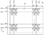
도 2는 실시 예에 정전기 방전회로를 포함하는 표시패널의 도면이다.
도 3은 실시 예에 따른 정전기 방전회로의 구성을 도시한 도면이다.
도 4는 실시 예에 따른 정전기 방전회로의 일 예를 도시한 도면이다.
도 5는 실시 예와 종래기술의 트랜지스터 턴-온 지연시간을 도시한 그래프이다.1 is a block diagram schematically showing a configuration of a display apparatus according to an embodiment of the present invention.
2 is a view of a display panel including an electrostatic discharge circuit in an embodiment.
3 is a diagram showing the configuration of the electrostatic discharge circuit according to the embodiment.
4 is a diagram showing an example of the electrostatic discharge circuit according to the embodiment.
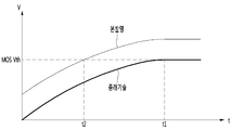
5 is a graph showing the transistor turn-on delay time of the embodiment and the prior art.
본 발명의 이점 및 특징, 그리고 그것들을 달성하는 방법은 첨부되는 도면과 함께 상세하게 후술되어 있는 실시 예들을 참조하면 명확해질 것이다. 그러나 본 발명은 이하에서 개시되는 실시 예들에 한정되는 것이 아니라 서로 다른 다양한 형태로 구현될 것이며, 단지 본 실시 예들은 본 발명의 개시가 완전하도록 하며, 본 발명이 속하는 기술 분야에서 통상의 지식을 가진 자에게 발명의 범주를 완전하게 알려주기 위해 제공되는 것이며, 본 발명은 청구항의 범주에 의해 정의될 뿐이다.BRIEF DESCRIPTION OF THE DRAWINGS The advantages and features of the present invention and the manner of achieving them will become apparent with reference to the embodiments described in detail below with reference to the accompanying drawings. The present invention may, however, be embodied in many different forms and should not be construed as being limited to the embodiments set forth herein. Rather, these embodiments are provided so that this disclosure will be thorough and complete, and will fully convey the concept of the invention to those skilled in the art. To fully disclose the scope of the invention to a person skilled in the art, and the invention is only defined by the scope of the claims.
본 발명의 실시 예를 설명하기 위한 도면에 개시된 형상, 크기, 비율, 각도, 개수 등은 예시적인 것이므로 본 발명이 도시된 사항에 한정되는 것은 아니다. 명세서 전체에 걸쳐 동일 참조 부호는 동일 구성 요소를 지칭한다. 또한, 본 발명을 설명함에 있어서, 관련된 공지 기술에 대한 구체적인 설명이 본 발명의 요지를 불필요하게 흐릴 수 있다고 판단되는 경우 그 상세한 설명은 생략한다.The shapes, sizes, ratios, angles, numbers, and the like disclosed in the drawings for describing the embodiments of the present invention are illustrative, and thus the present invention is not limited thereto. Like reference numerals refer to like elements throughout the specification. In the following description, well-known functions or constructions are not described in detail since they would obscure the invention in unnecessary detail.
본 명세서 상에서 언급한 '포함한다', '갖는다', '이루어진다' 등이 사용되는 경우 '~만'이 사용되지 않는 이상 다른 부분이 추가될 수 있다. 구성 요소를 단수로 표현한 경우에 특별히 명시적인 기재 사항이 없는 한 복수를 포함하는 경우를 포함한다.In the case where the word 'includes', 'having', 'done', etc. are used in this specification, other parts can be added unless '~ only' is used. Unless the context clearly dictates otherwise, including the plural unless the context clearly dictates otherwise.
구성 요소를 해석함에 있어서, 별도의 명시적 기재가 없더라도 오차 범위를 포함하는 것으로 해석한다.In interpreting the constituent elements, it is construed to include the error range even if there is no separate description.
위치 관계에 대한 설명일 경우, 예를 들어, '~상에', '~상부에', '~하부에', '~옆에' 등으로 두 부분의 위치 관계가 설명되는 경우, '바로' 또는 '직접'이 사용되지 않는 이상 두 부분 사이에 하나 이상의 다른 부분이 위치할 수도 있다.In the case of a description of the positional relationship, for example, if the positional relationship between two parts is described as 'on', 'on top', 'under', and 'next to' Or " direct " is not used, one or more other portions may be located between the two portions.
시간 관계에 대한 설명일 경우, 예를 들어, '~후에', '~에 이어서', '~다음에', '~전에' 등으로 시간 적 선후 관계가 설명되는 경우, '바로' 또는 '직접'이 사용되지 않는 이상 연속적이지 않은 경우도 포함할 수 있다.In the case of a description of a temporal relationship, for example, if a temporal posterior relationship is described by 'after', 'after', 'after', 'before', etc., 'May not be contiguous unless it is used.
제1, 제2 등이 다양한 구성요소들을 서술하기 위해서 사용되나, 이들 구성요소들은 이들 용어에 의해 제한되지 않는다. 이들 용어들은 단지 하나의 구성요소를 다른 구성요소와 구별하기 위하여 사용하는 것이다. 따라서, 이하에서 언급되는 제1 구성요소는 본 발명의 기술적 사상 내에서 제2 구성요소일 수도 있다.The first, second, etc. are used to describe various components, but these components are not limited by these terms. These terms are used only to distinguish one component from another. Therefore, the first component mentioned below may be the second component within the technical spirit of the present invention.
본 발명의 여러 실시 예들의 각각 특징들이 부분적으로 또는 전체적으로 서로 결합 또는 조합 가능하고, 기술적으로 다양한 연동 및 구동이 가능하며, 각 실시 예들이 서로에 대하여 독립적으로 실시 가능할 수도 있고 연관 관계로 함께 실시할 수도 있다.It is to be understood that each of the features of the various embodiments of the present invention may be combined or combined with each other, partially or wholly, technically various interlocking and driving, and that the embodiments may be practiced independently of each other, It is possible.
이하, 본 발명의 실시 예들은 도면을 참고하여 상세하게 설명한다. 그리고 도면들에 있어서, 장치의 크기 및 두께 등은 편의를 위하여 과장되어 표현될 수도 있다. 명세서 전체에 걸쳐서 동일한 참조번호들은 동일한 구성요소들을 나타낸다.Hereinafter, embodiments of the present invention will be described in detail with reference to the drawings. In the drawings, the size and thickness of the device may be exaggerated for convenience. Like reference numerals designate like elements throughout the specification.
도 1은 본 발명의 실시 예에 따른 표시장치의 구성을 개략적으로 도시한 블록도이고, 도 2는 실시 예에 정전기 방전회로를 포함하는 표시패널의 도면이다.Fig. 1 is a block diagram schematically showing a configuration of a display apparatus according to an embodiment of the present invention, and Fig. 2 is a diagram of a display panel including an electrostatic discharge circuit in an embodiment.
도 1 및 도 2에 도시된 바와 같이, 본 발명의 실시 예에 따른 표시장치는 표시패널(2), 타이밍 제어부(8), 데이터 드라이버(6) 및 게이트 드라이버(4)를 포함할 수 있다.1 and 2, the display device according to the embodiment of the present invention may include a
실시 예의 표시장치는 액정표시장치(LCD: Liquid Crystal Display, LCD)를 한정하여 설명하고 있지만, 이에 한정되는 것은 아니다. 예컨대 다른 예의 표시장치는 전계방출 표시장치(FED), 플라즈마 디스플레이 패널(PDP), 유기발광 다이오드 표시장치(OLED), 전기영동 표시장치(EPD)일 수 있다.A liquid crystal display (LCD) is limited to the display device of the embodiment, but the present invention is not limited thereto. For example, the display device of another example may be a field emission display (FED), a plasma display panel (PDP), an organic light emitting diode display (OLED), or an electrophoretic display (EPD).
상기 표시패널(2)은 서로 마주보는 제1 및 제2 유리기판과, 상기 제1 및 제2 유리기판 사이에 배치된 액정분자들을 포함한다. 상기 표시패널(2)은 데이터라인들(D1 내지 Dm)과 게이트 라인들(G1 내지 Gn)의 교차되어 매트릭스 구조를 갖고, m×n (m,n 은 양의 정수)개의 액정셀들(Clc)을 포함할 수 있다.The
상기 표시패널(2)의 제1 유리기판은 m 개의 데이터라인들(D1 내지 Dm), n개의 게이트 라인들(G1 내지 Gn), 데이터라인들(D1 내지 Dm)과 n개의 게이트 라인들(G1 내지 Gn)의 교차영역에 위치한 트랜지스터(TFT)들, 트랜지스터(TFT)들에 각각 접속된 액정셀, 화소전극, 및 스토리지 캐패시터(Cst)등을 포함할 수 있다.The first glass substrate of the
상기 표시패널(2)의 제2 유리기판 상에는 블랙매트릭스, 컬러필터 및 공통전극(Vcom)이 형성될 수 있다. 여기서, 상기 공통전극(Vcom)은 액정 구동방식에 따라 위치가 변경될 수 있다. 예컨대 상기 공통전극(Vcom)은 TN(Twisted Nematic) 모드와 VA(Vertical Alignment) 모드와 같은 수직전계 구동방식에서 제2 유리기판 상에 배치될 수 있고, IPS(In Plane Switching) 모드와 FFS(Fringe Field Switching) 모드와 같은 수평전계 구동방식에서 화소전극이 배치된 제1 유리기판 상에 배치될 수 있다.On the second glass substrate of the
상기 데이터 드라이버(6)는 타이밍 제어부(8)의 제어신호에 의해 디지털 비디오 데이터(RGB)를 래치할 수 있다. 상기 데이터 드라이버(6)는 상기 디지털 비디오 데이터를 아날로그 정극성/부극성 감마보상전압으로 변환하여 정극성/부극성 데이터전압을 발생하고 그 데이터전압을 데이터라인들(D1 내지 Dm)에 공급한다.The
상기 게이트 드라이버(4)는 타이밍 제어부(8)의 제어신호에 의해 1 수평기간의 펄스 폭을 가지는 게이트 신호들을 게이트 라인들(G1 내지 Gn)에 순차적으로 공급한다. 게이트 드라이버(4)는 화소 어레이와 동시에 제1 유리기판 상에 직접 형성될 수 있다.The
타이밍 제어부(8)는 외부 시스템으로부터 입력되는 디지털 비디오 데이터(RGB)를 표시패널(2)에 맞게 재정렬하여 데이터 드라이버(6)에 공급한다.The
타이밍 제어부(8)는 외부 시스템으로부터 수직/수평 동기신호(Vsync, Hsync), 데이터 인에이블(Data Enable), 클럭신호(CLK, MCLK와 같은 메인 클럭신호를 포함한다) 등의 타이밍 신호를 입력받아 데이터 드라이버(6)와 게이트 드라이버(4)의 동작 타이밍을 제어하기 위한 제어신호들을 생성한다.The
상기 데이터 드라이버(6)를 제어하기 위한 데이터 타이밍 제어신호는 데이터 스타트 펄스(SSP: Source Start Pulse), 데이터 샘플링 클럭(SSC: Source Sampling Clock), 극성제어신호(Pol: Polarity), 및 데이터 출력 인에이블신호(SOE: Source Output Enable) 등을 포함한다. 데이터 스타트 펄스(SSP)는 데이터 드라이버(6)의 데이터 샘플링 시작 타이밍을 제어한다.The data timing control signal for controlling the
데이터 샘플링 클럭(SSC)은 라이징 또는 폴링 에지에 기준하여 데이터 드라이버(122) 내에서 데이터의 샘플링 타이밍을 제어하는 클럭신호이다. 데이터 출력 인에이블신호(SOE)는 데이터 드라이버(6)의 출력 타이밍을 제어한다. 극성제어신호(POL)는 데이터 드라이버(6)로부터 출력되는 데이터전압의 수평 극성 반전 타이밍을 제어한다.The data sampling clock SSC is a clock signal that controls the sampling timing of data in the data driver 122 on the basis of the rising or falling edge. The data output enable signal SOE controls the output timing of the
게이트 드라이버(4)를 제어하기 위한 게이트 타이밍 제어신호는 게이트 스타트 펄스(GSP: Start Pulse), 게이트 시프트 클럭(GSC: Gate Shift Clock), 게이트 출력 인에이블 신호(GOE: Gate Output Enable) 등을 포함한다.The gate timing control signal for controlling the
실시 예의 표시패널(2)은 영상이 표시되는 표시영역(AA) 및 영상이 표시되지 않는 비표시영역(NA)을 포함할 수 있다. 상기 비표시영역(NA)은 상기 표시영역(AA)의 가장자리를 따라 배치될 수 있다.The
상기 비표시영역(NA)은 게이트 라인(G1 내지 Gn)과 연결되는 게이트 패드(12)와 데이터 라인(D1 내지 Dm)으로부터 연결된 데이터 패드(14)를 포함할 수 있다. 상기 게이트 패드(12)는 게이드 드라이버(4)의 입력패드로 정의할 수 있고, 데이터 패드(14)는 데이터 드라이버(6)의 입력패드으로 정의할 수 있다. 상기 게이트 라인(G1 내지 Gn) 및 데이터 라인(D1 내지 Dm)은 출력 라인으로 정의할 수 있다.The non-display area NA may include a
실시 예는 상기 게이트 패드(12)와 게이트 라인들 (G1 내지 Gn) 사이에 배치된 정전기 방전회로(20)를 포함할 수 있다. 실시 예는 상기 데이터 패드(14)와 데이터라인들(D1 내지 Dm) 사이에 배치된 정전기 방전회로(20)를 포함할 수 있으나, 이에 한정되는 것은 아니다.The embodiment may include an
상기 정전기 방전회로(20)는 상기 게이트 패드(12) 및 데이터 패드(14)로부터 입력되는 양(+)의 정전기(ESD) 또는 음(-)의 정전기(ESD)를 그라운드(GND) 라인으로 패스시킬 수 있다. 여기서, 상기 정전기 방전회로(20)는 양(+)의 정전기(ESD) 또는 음(-)의 정전기(ESD)로부터 표시패널(2)을 보호하여 양(+)의 정전기(ESD) 또는 음(-)의 정전기(ESD)에 의한 표시패널(2)의 수율저하를 개선할 수 있다.The
실시 예의 정전기 방전회로(20)는 양(+)의 정전기(ESD)를 그라운드(GND) 라인으로 패스시키는 제1 트랜지스터를 포함할 수 있다. 상기 정전기 방전회로(20)는 음(-)의 정전기(ESD)를 그라운드(GND) 라인으로 패스시키는 제2 트랜지스터를 포함할 수 있다. 상기 제1 및 제2 트랜지스터는 MOS 트랜지스터일 수 있으나, 이에 한정되는 것은 아니다.The
실시 예는 상기 제1 및 제2 트랜지스터의 응답속도를 향상시켜 양(+)의 정전기(ESD) 또는 음(-)의 정전기(ESD)로부터 정전기 내성을 확보할 수 있다. 즉, 실시 예는 정전기 방전회로(20)의 신뢰성을 향상시킬 수 있다.Embodiments can improve the response speed of the first and second transistors to secure electrostatic immunity from positive (ESD) or negative (ESD) static electricity. That is, the embodiment can improve the reliability of the
실시 예의 정전기 방전회로(20)는 도 2 내지 도 5를 참조하여 상세히 설명하도록 한다.The
도 3은 실시 예에 따른 정전기 방전회로의 구성을 도시한 도면이고, 도 4는 실시 예에 따른 정전기 방전회로의 일 예를 도시한 도면이고, 도 5는 실시 예와 종래기술의 트랜지스터 턴-온 지연시간을 도시한 그래프이다.FIG. 3 is a diagram showing the configuration of an electrostatic discharge circuit according to the embodiment, FIG. 4 is a diagram showing an example of the electrostatic discharge circuit according to the embodiment, Fig.
도 3 내지 도 5에 도시된 바와 같이, 실시 예의 정전기 방전회로(20)는 양(+)의 정전기(ESD)를 그라운드(GND)로 패스하는 제1 트랜지스터(M1)을 포함할 수 있다. 실시 예의 정전기 방전회로(20)는 음(-)의 정전기(ESD)를 그라운드(GND)로 패스하는 제2 트랜지스터(M2)를 포함할 수 있다. 상기 제1 및 제2 트랜지스터(M1, M2)는 MOS 트랜지스터일 수 있다. 실시 예의 상기 제1 및 제2 트랜지스터(M1, M2)는 NMOS 트랜지스터일 수 있으나, 이에 한정되는 것은 아니다. 3 to 5, the
실시 예는 상기 제1 및 제2 트랜지스터(M1, M2)의 게이트와 연결되는 배압부(21)를 포함할 수 있다. 상기 배압부(21)는 상기 제1 및 제2 트랜지스터(M1, M2)의 게이트 단자에 임의의 보상전압(Vout)을 제공하여 상기 제1 및 제2 트랜지스터(M1, M2)의 턴-온 타이밍을 줄이는 기능을 포함할 수 있다. 상기 배압부(21)는 입력전압을 이용하여 상기 제1 및 제2 트랜지스터(M1, M2)의 게이트 단자에 보상전압(Vout)을 제공할 수 있다. 상기 배압부(21)의 출력단은 상기 제1 및 제2 트랜지스터(M1, M2)의 게이트 단자와 연결될 수 있다. 여기서, 상기 제1 및 제2 트랜지스터(M1, M2)의 게이트 단자는 서로 연결될 수 있으나, 이에 한정되는 것은 아니다.The embodiment may include a
상기 정전기 방전회로(20)는 제1 트랜지스터(M1)의 게이트 단자와 상기 배압부(21)의 출력단 사이에 제2 다이오드(D2)를 포함할 수 있다. 상기 정전기 방전회로(20)는 제2 트랜지스터(M2)의 게이트 단자와 상기 배압부(21)의 출력단 사이에 제3 다이오드(D3)를 포함할 수 있다. 상기 제2 및 제3 다이오드(D2, D3)는 양(+)의 정전기(ESD) 또는 음(-)의 정전기(ESD)로부터 상기 배압부(21)를 보호하는 기능을 포함할 수 있다.The
상기 정전기 방전회로(20)는 제1 트랜지스터(M1)의 게이트 단자와 제1 노드(N1) 사이에 제1 다이오드(D1)를 포함할 수 있다. 여기서, 상기 제1 노드(N1)는 상기 게이트 패드(12) 또는 데이터 패드(14)와 게이트 라인(G1 내지 Gn) 또는 데이터 라인(D1 내지 Dm)의 출력라인상에 배치될 수 있다. 상기 제1 다이오드(D1)는 역전류 방지기능을 포함할 수 있다.The
상기 정전기 방전회로(20)는 제2 트랜지스터(D2)의 게이트 단자와 그라운드(GND) 사이에 제4 다이오드(D4)를 포함할 수 있다. 여기서, 상기 제2 트랜지스터(M2)의 드레인 단자는 제2 노드(N2)와 연결될 수 있다. 상기 제2 노드(N2)는 상기 제1 노드(N1)와 게이트 라인(G1 내지 Gn) 또는 데이터 라인(D1 내지 Dm)의 출력라인상에 배치될 수 있다. 상기 제4 다이오드(D4)는 역전류 방지기능을 포함할 수 있다.The
상기 배압부(21)는 상기 제1 및 제2 트랜지스터(M1, M2)의 게이트 단자에 상기 제1 및 제2 트랜지스터(M1, M2)의 문턱전압(MOS Vth)보다 낮은 전압레벨을 가질 수 있다. 예컨대 상기 배압부(21)의 보상전압(Vout)은 상기 제1 및 제2 트랜지스터(M1, M2)의 문턱전압(MOS Vth)의 50% 이상일 수 있다. 보다 구체적으로 상기 배압부(21)의 보상전압(Vout)은 상기 제1 및 제2 트랜지스터(M1, M2)의 문턱전압(MOS Vth)의 80% 일 수 있다. 상기 보상전입(Vout)이 상기 문턱전압(MOS Vth)의 50% 미만의 전압레벨을 갖는 경우, 상기 제1 및 제2 트랜지스터(M1, M2)의 턴-온 지연시간을 개선하기 어렵다. 상기 보상전입(Vout)이 상기 문턱전압(MOS Vth)의 80%를 초과하는 전압레벨을 갖는 경우, 정전기 방전회로(20)의 신뢰성이 저하될 수 있다.The
상기 배압부(21)는 보상전압 제어부(23), 제3 트랜지스터(M3), 인덕터(L), 제5 다이오드(D5) 및 캐패시터(C)를 포함할 수 있다. 상기 배압부(21)는 상기 제1 및 제2 노드(N1, N2) 사이의 제3 노드(N3)와 연결될 수 있다.The
상기 보상전압 제어부(23)는 입력전압을 이용하여 보상전압(Vout)을 생성하는 기준전압을 생성한다. 여기서, 입력전압의 전압레벨은 보상전압(Vout)의 전압레벨과 서로 대응되지 않는다.The
상기 인덕터(L)는 입력전압의 전류를 저장하고, 상기 제3 트랜지스터(M3)의 턴-온 시에 출력되는 보상전압(Vout)으로 승압하는 기능을 포함할 수 있다. 상기 인덕터(L)는 상기 제3 트랜지스터(M3)의 드레인 단자와 연결될 수 있다.The inductor L may include a function of storing a current of an input voltage and increasing the voltage of the third transistor M3 to a compensation voltage Vout that is output when the third transistor M3 is turned on. The inductor L may be connected to a drain terminal of the third transistor M3.
상기 제5 다이오드(D5)는 환류다이오드 기능을 포함할 수 있다. 즉, 상기 제5 다이오드(D5)는 제3 트랜지스터(M3)의 턴-오프 시에 상기 인턱터(L)의 역방향 기전력에 의한 임펄스 전압을 패스시킨다. 즉, 제5 다이오드(D5)는 제3 트랜지스터(M3)와 병렬 접속되어 상기 제3 트랜지스터(M3)를 보호하는 기능을 포함할 수 있다.The fifth diode D5 may include a reflux diode function. That is, the fifth diode D5 passes the impulse voltage due to the reverse electromotive force of the inductor L when the third transistor M3 is turned off. That is, the fifth diode D5 may be connected in parallel with the third transistor M3 to protect the third transistor M3.
상기 캐패시터(C)는 상기 보상전압(Vout)을 평활하는 기능을 포함할 수 있다. 상기 캐패시터(C)는 상기 제5 다이오드(D5)와 병렬 접속될 수 있다.The capacitor C may include a function of smoothing the compensation voltage Vout. The capacitor C may be connected in parallel with the fifth diode D5.
상기 보상전압 제어부(23)는 상기 제1 및 제2 트랜지스터(M1, M2)의 게이트 단자와 연결되는 제2 노드(N2)와 상기 제1 노드(N1) 사이의 제3 노드(N3)로부터 보상전압(Vout)을 제4 노드(N4)를 통해서 피드백하여 일정한 보상전압(Vout)을 유지할 수 있다. 상기 제4 노드(N4)는 제1 및 제2 트랜지스터(M1, M2)의 게이트 단자와 연결되는 배압부(21)의 출력단으로 정의되는 제5 노드(N5)와 연결될 수 있다.The
실시 예의 배압부(21)는 보상전압 제어부(23), 제3 트랜지스터(M3), 인덕터(L), 제5 다이오드(D5) 및 캐패시터(C)를 포함하는 구성으로 한정하여 설명하고 있지만, 이에 한정되는 것은 아니다.The
실시 예는 배압부(21)로부터 제1 및 제2 트랜지스터(M1, M2)의 게이트 단자에 제1 및 제2 트랜지스터(M1, M2)의 문턱전압(MOS Vth) 전압레벨의 80%의 보상전압(Vout)이 제공되어 일반적인 제1 및 제2 트랜지스터(M1, M2)의 턴-온 지연시간(t1) 보다 빠른 턴-온 지연시간(t2)을 구현할 수 있다. 따라서, 실시 예는 상기 제1 및 제2 트랜지스터(M1, M2)의 턴-온 지연시간을 줄여 양(+)의 정전기(ESD) 또는 음(-)의 정전기(ESD)로부터 표시패널(2)을 안전하게 보호할 수 있다.In the embodiment, a compensating voltage of 80% of the threshold voltage (MOS Vth) voltage level of the first and second transistors M1 and M2 is applied to the gate terminals of the first and second transistors M1 and M2 from the back- On delay time t2 which is earlier than the turn-on delay time t1 of the general first and second transistors M1 and M2 is provided. Therefore, the embodiment can reduce the turn-on delay time of the first and second transistors M1 and M2 to prevent the
실시 예는 입력전압을 이용하여 상기 제1 및 제2 트랜지스터(M1, M2)의 게이트 단자에 보상전압(Vout)을 일정하게 유지함으로써, 구동회로의 구성을 간소화할 수 있다.The embodiment can simplify the configuration of the driving circuit by keeping the compensation voltage Vout constant at the gate terminals of the first and second transistors M1 and M2 by using the input voltage.
표1은 ESD 유입시에 제1 및 제2 트랜지스터(M1, M2)의 턴-온 지연시간을 나타낸다.Table 1 shows the turn-on delay times of the first and second transistors M1 and M2 at the time of ESD input.
실시 예 1 내지 3은 보상전압(Vout) 1V 내지 3V이며, 제1 및 제2 트랜지스터(M1, M2)의 문턱전압(MOS Vth)은 4V일 수 있으나, 이에 한정되는 것은 아니다. 예컨대 상기 제1 및 제2 트랜지스터(M1, M2)의 문턱전압(MOS Vth)은 변경될 수 있고, 상기 제1 및 제2 트랜지스터(M1, M2)의 문턱전압(MOS Vth)에 따라 보상전압(Vout)도 변경될 수 있다.In
실시 예 1 내지 3은 일반적인 정전기 방전회로와 대비 최대 55%의 빠른 턴-온 지연시간을 구현할 수 있다.
실시 예는 상기 제1 및 제2 트랜지스터(M1, M2)의 문턱전압(MOS Vth)의 50% 이상의 보상전압(Vout)이 게이트 단자에 제공되어 상기 제1 및 제2 트랜지스터(M1, M2)의 턴-온 지연시간을 줄여 양(+)의 정전기(ESD) 또는 음(-)의 정전기(ESD)로부터 표시패널(2)을 안전하게 보호할 수 있다.A compensating voltage Vout of 50% or more of the threshold voltage (MOS Vth) of the first and second transistors M1 and M2 is provided to the gate terminal so that the voltage of the first and second transistors M1 and M2 It is possible to securely protect the
실시 예는 양(+)의 정전기(ESD) 또는 음(-)의 정전기(ESD) 유입시에 제1 및 제2 트랜지스터(M1, M2)의 빠른 턴-온 지연시간에 의해 양(+)의 정전기(ESD) 또는 음(-)의 정전기(ESD)로부터 구동회로를 안전하게 보호하므로 수율 향상 및 생산성을 향상시킬 수 있다.The embodiment is advantageous in that the positive turn-on delay time of the first and second transistors M1 and M2 at the time of positive (ESD) or negative (ESD) It is possible to safely protect the driving circuit from electrostatic (ESD) or negative (-) static electricity (ESD), thereby improving yield and productivity.
이상에서 실시 예들에 설명된 특징, 구조, 효과 등은 적어도 하나의 실시 예에 포함되며, 반드시 하나의 실시 예에만 한정되는 것은 아니다. 나아가, 각 실시 예에서 예시된 특징, 구조, 효과 등은 실시 예들이 속하는 분야의 통상의 지식을 가지는 자에 의해 다른 실시 예들에 대해서도 조합 또는 변형되어 실시 가능하다. 따라서 이러한 조합과 변형에 관계된 내용들은 실시 예의 범위에 포함되는 것으로 해석되어야 할 것이다.The features, structures, effects and the like described in the embodiments are included in at least one embodiment and are not necessarily limited to one embodiment. Further, the features, structures, effects, and the like illustrated in the embodiments can be combined and modified by other persons having ordinary skill in the art to which the embodiments belong. Accordingly, the contents of such combinations and modifications should be construed as being included in the scope of the embodiments.
이상에서 실시 예를 중심으로 설명하였으나 이는 단지 예시일 뿐 실시 예를 한정하는 것이 아니며, 실시 예가 속하는 분야의 통상의 지식을 가진 자라면 본 실시 예의 본질적인 특성을 벗어나지 않는 범위에서 이상에 예시되지 않은 여러 가지의 변형과 응용이 가능함을 알 수 있을 것이다. 예를 들어, 실시 예에 구체적으로 나타난 각 구성 요소는 변형하여 실시할 수 있는 것이다. 그리고 이러한 변형과 응용에 관계된 차이점들은 첨부된 청구 범위에서 설정하는 실시 예의 범위에 포함되는 것으로 해석되어야 할 것이다.While the present invention has been particularly shown and described with reference to exemplary embodiments thereof, it will be understood by those skilled in the art that various changes in form and details may be made therein without departing from the spirit and scope of the invention. It can be seen that the modification and application of branches are possible. For example, each component specifically shown in the embodiments can be modified and implemented. It is to be understood that the present invention may be embodied in many other specific forms without departing from the spirit or essential characteristics thereof.
20: 정전기 방전회로
21: 배압부
23: 보상전입 제어부
M1: 제1 트랜지스터
M2: 제2 트랜지스터
M3: 제3 트랜지스터20: Electrostatic discharge circuit
21:
23: compensation transfer control unit
M1: first transistor
M2: second transistor
M3: third transistor
Claims (7)
상기 입력패드와 연결된 출력라인;
상기 입력패드와 인접한 제1 노드와 연결된 제1 트랜지스터;
상기 출력라인과 인접한 제2 노드와 연결된 제2 트랜지스터; 및
상기 제1 및 제2 노드 사이의 제3 노드와 연결된 배압부를 포함하고, 상기 배압부는 상기 제1 및 제2 트랜지스터의 게이트 단자에 일정한 보상전압을 제공하는 정전기 방전회로.
Input pad;
An output line coupled to the input pad;
A first transistor coupled to a first node adjacent to the input pad;
A second transistor coupled to a second node adjacent to the output line; And
And a back pressure section connected to a third node between the first and second nodes, wherein the back pressure section provides a constant compensation voltage to the gate terminals of the first and second transistors.
상기 보상전압은 상기 제1 및 제2 트랜지스터의 문턱전압의 50% 이상의 전압레벨을 갖는 정전기 방전회로.
The method according to claim 1,
Wherein the compensation voltage has a voltage level of at least 50% of a threshold voltage of the first and second transistors.
상기 보상전압은 상기 제1 및 제2 트랜지스터의 문턱전압의 80%의 전압레벨을 갖는 정전기 방전회로.
The method according to claim 1,
Wherein the compensation voltage has a voltage level of 80% of a threshold voltage of the first and second transistors.
상기 제1 노드와 상기 제1 트랜지스터의 게이트 단자와 연결된 제1 다이오드; 및
상기 제2 트랜지스터의 게이트 단자와 그라운드 사이에 연결된 제4 다이오드를 포함하는 정전기 방전회로.
The method according to claim 1,
A first diode connected to the gate terminal of the first transistor and the first node; And
And a fourth diode connected between the gate terminal of the second transistor and ground.
상기 제1 트랜지스터의 게이트 단자와 상기 배압부 사이에 연결된 제2 다이오드; 및
상기 제2 트랜지스터의 게이트 단자와 상기 배압부 상에 연결된 제3 다이오드를 포함하는 정전기 방전회로.
The method according to claim 1,
A second diode connected between the gate terminal of the first transistor and the back pressure portion; And
And a third diode coupled to the gate terminal of the second transistor and the backpressure portion.
상기 배압부는,
상기 제3 노드와 연결되는 보상전압 제어부;
상기 제3 노드와 연결된 인덕터;
상기 보상저압 제어부의 제어신호에 의해 턴-온되는 제3 트랜지스터;
상기 제3 트랜지스터와 병렬 접속된 제5 다이오드; 및
상기 제5 다이오드와 병렬 접속되는 캐패시터를 포함하는 정전기 방전회로.
The method according to claim 1,
The back-
A compensation voltage control unit connected to the third node;
An inductor coupled to the third node;
A third transistor that is turned on by a control signal of the compensation low voltage control unit;
A fifth diode connected in parallel with the third transistor; And
And a capacitor connected in parallel with the fifth diode.
상기 출력라인으로부터 입력된 구동신호에 의해 영상이 디스플레이되는 표시패널을 포함하는 표시장치. An electrostatic discharge circuit according to any one of claims 1 to 6; And
And a display panel in which an image is displayed by a drive signal input from the output line.
Priority Applications (1)
| Application Number | Priority Date | Filing Date | Title |
|---|---|---|---|
| KR1020150187841A KR102397866B1 (en) | 2015-12-28 | 2015-12-28 | Electostatic discharge circuit and display device having the same |
Applications Claiming Priority (1)
| Application Number | Priority Date | Filing Date | Title |
|---|---|---|---|
| KR1020150187841A KR102397866B1 (en) | 2015-12-28 | 2015-12-28 | Electostatic discharge circuit and display device having the same |
Publications (2)
| Publication Number | Publication Date |
|---|---|
| KR20170077681A true KR20170077681A (en) | 2017-07-06 |
| KR102397866B1 KR102397866B1 (en) | 2022-05-12 |
Family
ID=59354500
Family Applications (1)
| Application Number | Title | Priority Date | Filing Date |
|---|---|---|---|
| KR1020150187841A Active KR102397866B1 (en) | 2015-12-28 | 2015-12-28 | Electostatic discharge circuit and display device having the same |
Country Status (1)
| Country | Link |
|---|---|
| KR (1) | KR102397866B1 (en) |
Cited By (4)
| Publication number | Priority date | Publication date | Assignee | Title |
|---|---|---|---|---|
| US10930231B2 (en) | 2018-03-27 | 2021-02-23 | Samsung Electronics Co., Ltd. | Display module including electro-static discharge protection circuit |
| CN113160762A (en) * | 2020-01-07 | 2021-07-23 | 京东方科技集团股份有限公司 | Bias compensation circuit of transistor, driving method of bias compensation circuit and display substrate |
| US11556025B2 (en) | 2019-10-08 | 2023-01-17 | Samsung Display Co., Ltd. | Display panel |
| WO2024174814A1 (en) * | 2023-02-21 | 2024-08-29 | 京东方科技集团股份有限公司 | Display panel and display apparatus |
Citations (7)
| Publication number | Priority date | Publication date | Assignee | Title |
|---|---|---|---|---|
| KR20070070966A (en) * | 2005-12-29 | 2007-07-04 | 주식회사 하이닉스반도체 | Electrostatic discharge protection circuit |
| KR20070088060A (en) * | 2006-02-24 | 2007-08-29 | 주식회사 하이닉스반도체 | Electrostatic Protection Devices for Semiconductor Devices |
| KR100861310B1 (en) * | 2007-07-20 | 2008-10-01 | 주식회사 하이닉스반도체 | Electrostatic discharge device |
| KR20130059506A (en) * | 2011-11-29 | 2013-06-07 | 엘지디스플레이 주식회사 | Liquid crystal display device |
| KR20130059508A (en) * | 2011-11-29 | 2013-06-07 | 엘지디스플레이 주식회사 | Liquid crystal display device |
| JP2014523145A (en) * | 2011-08-05 | 2014-09-08 | アーエムエス アクチエンゲゼルシャフト | Circuit device for electrostatic discharge protection |
| KR20150070020A (en) * | 2013-12-13 | 2015-06-24 | 아이엠이씨 브이제트더블유 | Restoring off-state stress degradation of threshold voltage |
-
2015
- 2015-12-28 KR KR1020150187841A patent/KR102397866B1/en active Active
Patent Citations (7)
| Publication number | Priority date | Publication date | Assignee | Title |
|---|---|---|---|---|
| KR20070070966A (en) * | 2005-12-29 | 2007-07-04 | 주식회사 하이닉스반도체 | Electrostatic discharge protection circuit |
| KR20070088060A (en) * | 2006-02-24 | 2007-08-29 | 주식회사 하이닉스반도체 | Electrostatic Protection Devices for Semiconductor Devices |
| KR100861310B1 (en) * | 2007-07-20 | 2008-10-01 | 주식회사 하이닉스반도체 | Electrostatic discharge device |
| JP2014523145A (en) * | 2011-08-05 | 2014-09-08 | アーエムエス アクチエンゲゼルシャフト | Circuit device for electrostatic discharge protection |
| KR20130059506A (en) * | 2011-11-29 | 2013-06-07 | 엘지디스플레이 주식회사 | Liquid crystal display device |
| KR20130059508A (en) * | 2011-11-29 | 2013-06-07 | 엘지디스플레이 주식회사 | Liquid crystal display device |
| KR20150070020A (en) * | 2013-12-13 | 2015-06-24 | 아이엠이씨 브이제트더블유 | Restoring off-state stress degradation of threshold voltage |
Cited By (7)
| Publication number | Priority date | Publication date | Assignee | Title |
|---|---|---|---|---|
| US10930231B2 (en) | 2018-03-27 | 2021-02-23 | Samsung Electronics Co., Ltd. | Display module including electro-static discharge protection circuit |
| US11238818B2 (en) | 2018-03-27 | 2022-02-01 | Samsung Electronics Co., Ltd. | Display module including electro-static discharge protection circuit |
| US11556025B2 (en) | 2019-10-08 | 2023-01-17 | Samsung Display Co., Ltd. | Display panel |
| US11835807B2 (en) | 2019-10-08 | 2023-12-05 | Samsung Display Co., Ltd. | Display panel |
| US12535703B2 (en) | 2019-10-08 | 2026-01-27 | Samsung Display Co., Ltd. | Display panel |
| CN113160762A (en) * | 2020-01-07 | 2021-07-23 | 京东方科技集团股份有限公司 | Bias compensation circuit of transistor, driving method of bias compensation circuit and display substrate |
| WO2024174814A1 (en) * | 2023-02-21 | 2024-08-29 | 京东方科技集团股份有限公司 | Display panel and display apparatus |
Also Published As
| Publication number | Publication date |
|---|---|
| KR102397866B1 (en) | 2022-05-12 |
Similar Documents
| Publication | Publication Date | Title |
|---|---|---|
| US9910329B2 (en) | Liquid crystal display device for cancelling out ripples generated the common electrode | |
| US9818362B2 (en) | Charging scan and charge sharing scan double output GOA circuit | |
| US20140043306A1 (en) | Liquid crystal display device | |
| US20150243238A1 (en) | Display device | |
| KR102281753B1 (en) | Stage circuit and scan driver using the same | |
| KR101991674B1 (en) | Liquid crystal display device | |
| KR20140131137A (en) | Shift register and flat panel display device using the same | |
| KR102394393B1 (en) | Display device | |
| KR102397866B1 (en) | Electostatic discharge circuit and display device having the same | |
| KR20150044514A (en) | Liquid crystal display device | |
| US11468812B2 (en) | Display apparatus | |
| KR20150106304A (en) | Electrostatic Discharge Circuit And Liquid Crystal Display Device Comprising The Same | |
| KR20140022710A (en) | Liquid crystal display device | |
| KR101980749B1 (en) | Display device | |
| KR102211065B1 (en) | Display device | |
| KR102429388B1 (en) | Protective circuit and display device having the same | |
| US8441431B2 (en) | Backlight unit and liquid crystal display using the same | |
| KR102148488B1 (en) | Power Supply Circuit of Display Device | |
| KR102277714B1 (en) | Gate Driver and Display Device having thereof | |
| KR101862609B1 (en) | Liquid crystal display device | |
| KR102283377B1 (en) | Display device and gate driving circuit thereof | |
| KR20140078203A (en) | Liquid crystal display device and driving method thereof | |
| KR101944047B1 (en) | Liquid crystal display device | |
| KR102016566B1 (en) | Liquid crystal display device | |
| KR101920757B1 (en) | Liquid crystal display device |
Legal Events
| Date | Code | Title | Description |
|---|---|---|---|
| PA0109 | Patent application |
St.27 status event code: A-0-1-A10-A12-nap-PA0109 |
|
| R17-X000 | Change to representative recorded |
St.27 status event code: A-3-3-R10-R17-oth-X000 |
|
| PG1501 | Laying open of application |
St.27 status event code: A-1-1-Q10-Q12-nap-PG1501 |
|
| P22-X000 | Classification modified |
St.27 status event code: A-2-2-P10-P22-nap-X000 |
|
| A201 | Request for examination | ||
| PA0201 | Request for examination |
St.27 status event code: A-1-2-D10-D11-exm-PA0201 |
|
| E701 | Decision to grant or registration of patent right | ||
| PE0701 | Decision of registration |
St.27 status event code: A-1-2-D10-D22-exm-PE0701 |
|
| GRNT | Written decision to grant | ||
| PR0701 | Registration of establishment |
St.27 status event code: A-2-4-F10-F11-exm-PR0701 |
|
| PR1002 | Payment of registration fee |
St.27 status event code: A-2-2-U10-U11-oth-PR1002 Fee payment year number: 1 |
|
| PG1601 | Publication of registration |
St.27 status event code: A-4-4-Q10-Q13-nap-PG1601 |
|
| PR1001 | Payment of annual fee |
St.27 status event code: A-4-4-U10-U11-oth-PR1001 Fee payment year number: 4 |
|
| PR1001 | Payment of annual fee |
St.27 status event code: A-4-4-U10-U11-oth-PR1001 Fee payment year number: 5 |
|
| U11 | Full renewal or maintenance fee paid |
Free format text: ST27 STATUS EVENT CODE: A-4-4-U10-U11-OTH-PR1001 (AS PROVIDED BY THE NATIONAL OFFICE) Year of fee payment: 5 |