KR20170077689A - Method and devices for reducing PAPR - Google Patents
Method and devices for reducing PAPR Download PDFInfo
- Publication number
- KR20170077689A KR20170077689A KR1020150187859A KR20150187859A KR20170077689A KR 20170077689 A KR20170077689 A KR 20170077689A KR 1020150187859 A KR1020150187859 A KR 1020150187859A KR 20150187859 A KR20150187859 A KR 20150187859A KR 20170077689 A KR20170077689 A KR 20170077689A
- Authority
- KR
- South Korea
- Prior art keywords
- signal
- input signal
- digital
- filter
- digital signal
- Prior art date
- Legal status (The legal status is an assumption and is not a legal conclusion. Google has not performed a legal analysis and makes no representation as to the accuracy of the status listed.)
- Ceased
Links
Images


Classifications
-
- H—ELECTRICITY
- H04—ELECTRIC COMMUNICATION TECHNIQUE
- H04B—TRANSMISSION
- H04B7/00—Radio transmission systems, i.e. using radiation field
- H04B7/14—Relay systems
- H04B7/15—Active relay systems
-
- H—ELECTRICITY
- H04—ELECTRIC COMMUNICATION TECHNIQUE
- H04L—TRANSMISSION OF DIGITAL INFORMATION, e.g. TELEGRAPHIC COMMUNICATION
- H04L27/00—Modulated-carrier systems
- H04L27/26—Systems using multi-frequency codes
- H04L27/2601—Multicarrier modulation systems
- H04L27/2614—Peak power aspects
- H04L27/2623—Reduction thereof by clipping
-
- H—ELECTRICITY
- H04—ELECTRIC COMMUNICATION TECHNIQUE
- H04L—TRANSMISSION OF DIGITAL INFORMATION, e.g. TELEGRAPHIC COMMUNICATION
- H04L25/00—Baseband systems
- H04L25/02—Details ; arrangements for supplying electrical power along data transmission lines
- H04L25/20—Repeater circuits; Relay circuits
-
- H—ELECTRICITY
- H04—ELECTRIC COMMUNICATION TECHNIQUE
- H04L—TRANSMISSION OF DIGITAL INFORMATION, e.g. TELEGRAPHIC COMMUNICATION
- H04L27/00—Modulated-carrier systems
- H04L27/26—Systems using multi-frequency codes
- H04L27/2601—Multicarrier modulation systems
- H04L27/2614—Peak power aspects
- H04L27/2623—Reduction thereof by clipping
- H04L27/2624—Reduction thereof by clipping by soft clipping
-
- H—ELECTRICITY
- H04—ELECTRIC COMMUNICATION TECHNIQUE
- H04L—TRANSMISSION OF DIGITAL INFORMATION, e.g. TELEGRAPHIC COMMUNICATION
- H04L27/00—Modulated-carrier systems
- H04L27/26—Systems using multi-frequency codes
- H04L27/2601—Multicarrier modulation systems
- H04L27/2647—Arrangements specific to the receiver only
- H04L27/2655—Synchronisation arrangements
- H04L27/2689—Link with other circuits, i.e. special connections between synchronisation arrangements and other circuits for achieving synchronisation
- H04L27/2695—Link with other circuits, i.e. special connections between synchronisation arrangements and other circuits for achieving synchronisation with channel estimation, e.g. determination of delay spread, derivative or peak tracking
-
- H—ELECTRICITY
- H04—ELECTRIC COMMUNICATION TECHNIQUE
- H04W—WIRELESS COMMUNICATION NETWORKS
- H04W52/00—Power management, e.g. Transmission Power Control [TPC] or power classes
- H04W52/04—Transmission power control [TPC]
- H04W52/30—Transmission power control [TPC] using constraints in the total amount of available transmission power
- H04W52/36—Transmission power control [TPC] using constraints in the total amount of available transmission power with a discrete range or set of values, e.g. step size, ramping or offsets
-
- H—ELECTRICITY
- H03—ELECTRONIC CIRCUITRY
- H03H—IMPEDANCE NETWORKS, e.g. RESONANT CIRCUITS; RESONATORS
- H03H17/00—Networks using digital techniques
- H03H2017/0072—Theoretical filter design
- H03H2017/0081—Theoretical filter design of FIR filters
Landscapes
- Engineering & Computer Science (AREA)
- Computer Networks & Wireless Communication (AREA)
- Signal Processing (AREA)
- Noise Elimination (AREA)
- Power Engineering (AREA)
- Cable Transmission Systems, Equalization Of Radio And Reduction Of Echo (AREA)
Abstract
PAPR을 감소시키기 위한 방법이 개시된다. 본 발명의 일 실시예에 따른 PAPR을 감소시키기 위한 방법은 입력 신호를 클리핑(clipping)하는 단계, 입력 신호를 지연시키는 단계, 지연된 입력 신호에서 클리핑된 입력 신호를 감산하는 단계, 입력 신호의 클리핑에 의해 생성되는 에러(error)를 세이프(shape)하기 위해 감산된 신호를 필터링하는 단계, 입력 신호의 노이즈(noise)를 제거하기 위해 입력 신호를 필터링하는 단계 및 필터링된 입력 신호에서 필터링된 감산된 신호를 감산하는 단계를 포함한다.A method for reducing PAPR is disclosed. A method for reducing PAPR in accordance with an embodiment of the present invention includes clipping an input signal, delaying the input signal, subtracting the clipped input signal from the delayed input signal, Filtering the subtracted signal to shape the error produced by the subtracted signal, filtering the input signal to remove noise of the input signal, and filtering the subtracted signal .
Description
본 발명은 PAPR(Peak to Average Power Ration)을 감소시키기 위한 방법 및 장치들에 관한 것으로서, 보다 상세하게는 중계기(repeater)의 전력 효율성을 높이기 위한 PAPR(Peak to Average Power Ration)을 감소시키기 위한 방법 및 장치들에 관한 것이다.
The present invention relates to a method and apparatus for reducing Peak to Average Power Ratio (PAPR), and more particularly, to a method for reducing Peak to Average Power Ratio (PAPR) for increasing power efficiency of a repeater And devices.
중계기는 신호를 수신하여 더 높은 레벨 또는 더 높은 전력(power)으로 상기 신호를 재송신하는 전자 장치이다. A repeater is an electronic device that receives a signal and retransmits the signal at a higher level or higher power.
중계기에서 이용되는 신호는 종종 높은 PAPR(Peak to Average Power Ratio)을 가진다. 이는 중계기에서 구현되는 전력 증폭기(Power Amplifier)의 효율성을 제한시킨다. 따라서 전력 증폭기의 효율성을 높이기 위해 여러 가지 PAPR 감소 방법들이 제안되고 있다. Signals used in repeaters often have a high Peak to Average Power Ratio (PAPR). This limits the efficiency of the Power Amplifier implemented in the repeater. Therefore, various PAPR reduction methods have been proposed to increase the efficiency of the power amplifier.
CFR(Crest Factor Reduction)이 그 방법들 중 하나이다. 하지만, 종래의 CFR 기법은 중계기의 지연 시간을 증가시키는 문제점이 있었다.
Crest Factor Reduction (CFR) is one of those methods. However, the conventional CFR technique has a problem of increasing the delay time of the repeater.
본 발명은 PAPR을 감소시킴과 동시에 중계기의 지연 시간을 최소화시키기 위한 PAPR(Peak to Average Power Ration)를 감소시키기 위한 방법 및 장치들을 제공하고자 한다.
SUMMARY OF THE INVENTION The present invention seeks to provide a method and apparatus for reducing Peak to Average Power Ratio (PAPR) for reducing PAPR and minimizing the delay time of a repeater.
본 발명의 일 측면에 따르면, 입력 신호를 클리핑하는 단계, 상기 입력 신호를 지연시키는 단계, 상기 지연된 입력 신호에서 상기 클리핑된 입력 신호를 감산하는 단계, 상기 입력 신호의 클리핑에 의해 생성되는 에러를 세이프하기 위해 상기 감산된 신호를 필터링하는 단계, 상기 입력 신호의 노이즈를 제거하기 위해 상기 입력 신호를 필터링하는 단계, 및 상기 필터링된 입력 신호에서 상기 필터링된 감산된 신호를 감산하는 단계를 포함하는 PAPR을 감소시키기 위한 방법이 제공된다. According to an aspect of the present invention there is provided a method of generating a delayed input signal by clipping an input signal, delaying the input signal, subtracting the clipped input signal from the delayed input signal, Filtering the input signal to remove noise in the input signal, and subtracting the filtered subtracted signal from the filtered input signal to obtain a filtered output signal, / RTI >
실시예에 따라서, 상기 입력 신호를 필터링하기 위해 소요되는 시간은, 상기 입력 신호를 지연시키기 위해 소요되는 시간, 상기 지연된 입력 신호에서 상기 클리핑된 입력 신호를 감산하기 위해 소요되는 시간, 및 상기 감산된 신호를 필터링하기 위해 소요되는 시간의 합산 시간과 같을 수 있다. According to an embodiment, the time taken to filter the input signal is determined by the time it takes to delay the input signal, the time taken to subtract the clipped input signal from the delayed input signal, May be equal to the sum of the time taken to filter the signal.
실시예에 따라서, 상기 클리핑된 입력 신호의 레벨은 문턱 값 이하일 수 있다.
According to an embodiment, the level of the clipped input signal may be less than or equal to a threshold value.
본 발명의 다른 측면에 따르면, 입력 신호를 클리핑하는 클리퍼, 상기 입력 신호를 지연시키는 딜레이 유닛, 상기 지연된 입력 신호에서 상기 클리핑된 입력 신호를 감산하는 제1감산기, 상기 입력 신호의 클리핑에 의해 생성되는 에러를 세이프(shape)하기 위해 상기 감산된 신호를 필터링하는 에러 세이핑 필터, 상기 입력 신호의 노이즈를 제거하기 위해 상기 입력 신호를 필터링하는 디지털 필터, 및 상기 필터링된 입력 신호에서 상기 필터링된 감산된 신호를 감산하는 제2감산기를 포함하는 CFR 코어가 제공된다. According to another aspect of the present invention, there is provided a digital signal processor comprising: a clipper for clipping an input signal; a delay unit for delaying the input signal; a first subtractor for subtracting the clipped input signal from the delayed input signal; An error clearing filter for filtering the subtracted signal to shape an error, a digital filter for filtering the input signal to remove noise of the input signal, and a subtracter for subtracting the filtered subtracted A CFR core is provided that includes a second subtractor for subtracting the signal.
실시예에 따라서, 상기 입력 신호를 필터링하기 위해 소요되는 시간은, 상기 입력 신호를 지연시키기 위해 소요되는 시간, 상기 지연된 입력 신호에서 상기 클리핑된 입력 신호를 감산하기 위해 소요되는 시간, 및 상기 감산된 신호를 필터링하기 위해 소요되는 시간의 합산 시간과 같을 수 있다. According to an embodiment, the time taken to filter the input signal is determined by the time it takes to delay the input signal, the time taken to subtract the clipped input signal from the delayed input signal, May be equal to the sum of the time taken to filter the signal.
실시예에 따라서, 상기 에러 세이핑 필터는 FIR(Finite Impulse Response) 필터일 수 있다.According to an embodiment, the error-eliminating filter may be a Finite Impulse Response (FIR) filter.
실시예에 따라서, 상기 디지털 필터는 FIR(Finite Impulse Response) 필터일 수 있다.
According to an embodiment, the digital filter may be a Finite Impulse Response (FIR) filter.
본 발명의 또 다른 실시예에 따르면, 제1아날로그 신호를 수신하는 제1안테나, 상기 제1아날로그 신호를 제1디지털 신호로 변환하는 ADC(Analog to Digital Converter), 상기 제1디지털 신호를 수신하여 PAPR이 감소된 제2디지털 신호로 출력하는 CFR 코어, 상기 제2디지털 신호를 제2아날로그 신호로 변환하는 DAC(Digital to Analog Converter), 및 상기 제2아날로그 신호를 송신하는 제2안테나를 포함하는 중계기가 제공된다. According to another embodiment of the present invention, there is provided a digital signal processing apparatus including a first antenna for receiving a first analog signal, an ADC (Analog to Digital Converter) for converting the first analog signal into a first digital signal, A CFR core outputting a second digital signal with a reduced PAPR, a digital to analog converter (DAC) converting the second digital signal to a second analog signal, and a second antenna transmitting the second analog signal A repeater is provided.
실시예에 따라서, 상기 CFR 코어는 상기 제1디지털 신호를 클리핑하는 클리퍼, 상기 제1디지털 신호를 지연시키는 딜레이 유닛, 상기 지연된 제1디지털 신호에서 상기 클리핑된 제1디지털 신호를 감산하는 제1감산기, 상기 제1디지털 신호의 클리핑에 의해 생성되는 에러를 세이프하기 위해 상기 감산된 신호를 필터링하는 에러 세이핑 필터, 상기 제1디지털 신호의 노이즈를 제거하기 위해 상기 제1디지털 신호를 필터링하는 디지털 필터, 및 상기 필터링된 제1디지털 신호에서 상기 필터링된 감산된 신호를 감산하는 제2감산기를 포함할 수 있다. According to an embodiment, the CFR core includes a clipper for clipping the first digital signal, a delay unit for delaying the first digital signal, a first subtracter for subtracting the clipped first digital signal from the delayed first digital signal, An error clearing filter for filtering the subtracted signal to safeguard an error caused by clipping of the first digital signal, a digital filter for filtering the first digital signal to remove noise of the first digital signal, And a second subtractor for subtracting the filtered subtracted signal from the filtered first digital signal.
실시예에 따라서, 상기 제1디지털 신호를 필터링하기 위해 소요되는 시간은, 상기 제1디지털 신호를 지연시키기 위해 소요되는 시간, 상기 지연된 제1디지털 신호에서 상기 클리핑된 제1디지털 신호를 감산하기 위해 소요되는 시간, 및 상기 감산된 신호를 필터링하기 위해 소요되는 시간의 합산 시간과 같을 수 있다. According to an embodiment, the time taken to filter the first digital signal is determined by the time required to delay the first digital signal, the time required to subtract the clipped first digital signal from the delayed first digital signal And the time required to filter the subtracted signal.
실시예에 따라서, 상기 에러 세이핑 필터는 FIR 필터일 수 있다.
According to an embodiment, the error-eliminating filter may be an FIR filter.
본 발명의 기술적 사상에 의한 실시예들에 따른 PAPR(Peak to Average Power Ration)를 감소시키기 위한 방법 및 장치들은 딜레이 유닛(delay unit) 대신에 디지털 필터(digital filter)를 이용함으로써 PAPR을 감소시킴과 동시에 중계기의 지연 시간이 최소화될 수 있다.
The methods and apparatuses for reducing Peak to Average Power Ratio (PAPR) according to embodiments of the present invention can reduce PAPR by using a digital filter instead of a delay unit, At the same time, the delay time of the repeater can be minimized.
도 1은 본 발명의 실시예에 따른 무선 통신 시스템의 블록도이다.
도 2는 도 1에 도시된 중계기의 블록도이다.
도 3은 도 2에 도시된 CFR(Crest Factor Reduction) 코어의 블록도이다.
도 4는 도 2에 도시된 CFR(Crest Factor Reduction) 코어의 동작을 설명하기 위한 흐름도이다.1 is a block diagram of a wireless communication system according to an embodiment of the present invention.
2 is a block diagram of the repeater shown in FIG.
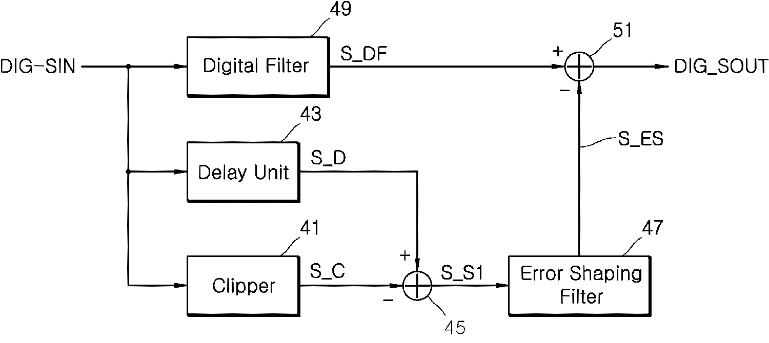
3 is a block diagram of the CFR (Crest Factor Reduction) core shown in FIG.
4 is a flowchart for explaining the operation of the CFR (Crest Factor Reduction) core shown in FIG.
본 발명은 다양한 변경을 가할 수 있고 여러 가지 실시예를 가질 수 있는 바, 특정 실시예들을 도면에 예시하고 이를 상세한 설명을 통해 상세히 설명하고자 한다. 그러나, 이는 본 발명을 특정한 실시 형태에 대해 한정하려는 것이 아니며, 본 발명의 사상 및 기술 범위에 포함되는 모든 변경, 균등물 내지 대체물을 포함하는 것으로 이해되어야 한다.While the present invention has been described in connection with certain exemplary embodiments, it is to be understood that the invention is not limited to the disclosed embodiments, but, on the contrary, is intended to cover various modifications and similarities. It should be understood, however, that the invention is not intended to be limited to the particular embodiments, but includes all modifications, equivalents, and alternatives falling within the spirit and scope of the invention.
본 발명을 설명함에 있어서, 관련된 공지 기술에 대한 구체적인 설명이 본 발명의 요지를 불필요하게 흐릴 수 있다고 판단되는 경우 그 상세한 설명을 생략한다. 또한, 본 명세서의 설명 과정에서 이용되는 숫자(예를 들어, 제1, 제2 등)는 하나의 구성요소를 다른 구성요소와 구분하기 위한 식별기호에 불과하다. 또한, 본 명세서에서, 일 구성요소가 다른 구성요소와 "연결된다" 거나 "접속된다" 등으로 언급된 때에는, 상기 일 구성요소가 상기 다른 구성요소와 직접 연결되거나 또는 직접 접속될 수도 있지만, 특별히 반대되는 기재가 존재하지 않는 이상, 중간에 또 다른 구성요소를 매개하여 연결되거나 또는 접속될 수도 있다고 이해되어야 할 것이다. 또한, 본 명세서에 기재된 "~부(유닛)", "~기", "~자", "~모듈" 등의 용어는 적어도 하나의 기능이나 동작을 처리하는 단위를 의미하며, 이는 하드웨어나 소프트웨어 또는 하드웨어 및 소프트웨어의 결합으로 구현될 수 있다. DETAILED DESCRIPTION OF THE PREFERRED EMBODIMENTS Hereinafter, the present invention will be described in detail with reference to the accompanying drawings. In addition, numerals (e.g., first, second, etc.) used in the description of the present invention are merely an identifier for distinguishing one component from another. Also, in this specification, when an element is referred to as being "connected" or "connected" with another element, the element may be directly connected or directly connected to the other element, It should be understood that, unless an opposite description is present, it may be connected or connected via another element in the middle. It should be noted that the terms such as " unit, "" to, "and" to module ", as used herein, mean units for processing at least one function or operation, Or a combination of hardware and software.
그리고 본 명세서에서의 구성부들에 대한 구분은 각 구성부가 담당하는 주기능 별로 구분한 것에 불과함을 명확히 하고자 한다. 즉, 이하에서 설명할 2개 이상의 구성부가 하나의 구성부로 합쳐지거나 또는 하나의 구성부가 보다 세분화된 기능별로 2개 이상으로 분화되어 구비될 수도 있다. 그리고 이하에서 설명할 구성부 각각은 자신이 담당하는 주기능 이외에도 다른 구성부가 담당하는 기능 중 일부 또는 전부의 기능을 추가적으로 수행할 수도 있으며, 구성부 각각이 담당하는 주기능 중 일부 기능이 다른 구성부에 의해 전담되어 수행될 수도 있음은 물론이다. 이하, 본 발명의 실시예들을 차례로 상세히 설명한다.
It is to be clarified that the division of constituent parts in this specification is merely a division by each main function of each constituent part. That is, two or more constituent parts to be described below may be combined into one constituent part, or one constituent part may be divided into two or more functions according to functions that are more subdivided. In addition, each of the constituent units described below may additionally perform some or all of the functions of other constituent units in addition to the main functions of the constituent units themselves, and that some of the main functions, And may be carried out in a dedicated manner. Hereinafter, embodiments of the present invention will be described in detail.
도 1은 본 발명의 실시 예에 따른 무선 통신 시스템의 블록도를 나타낸다. 1 shows a block diagram of a wireless communication system according to an embodiment of the present invention.
도 1을 참조하면, 무선 통신 시스템(400)은 주파수 분할 듀플렉싱(Frequency Division Duplexing; FDD) 네트워크, 주파수 분할 다중 액세스(Frequency Division Multiple Access; FDMA) 네트워크, 직교 FDMA(Orthogonal FDMA; OFDMA) 네트워크, 코드 분할 다중 액세스(Code Division Multiple Access; CDMA) 네트워크, 시 분할 다중 액세스(Time Division Multiple Access; TDMA) 네트워크, 직접 시퀀스 확산 스펙트럼(Direct Sequence Spread Spectrum; DSSS) 네트워크, 주파수 호핑 확산 스펙트럼(Hopping Spread Spectrum; FHSS) 네트워크, 또는 어떤 다른 무선 통신 네트워크를 포함할 수 있다. 일부 실시예들에서, 무선 통신 시스템(100)은 제2세대(2G) 무선 통신 네트워크, 제3세대(3G) 무선 통신 네트워크, 제4세대(4G) 무선 통신 네트워크, 또는 롱텀 에볼루션(Long Term Evolution; LTE) 무선 통신 네트워크로서 동작하도록 구성될 수 있다. 1, a
무선 통신 시스템(400)은 중계기(100), 기지국(base station; 200), 및 통신 장치(300)를 포함할 수 있다. The
기지국(200)과 통신 장치(300)는 신호를 주고 받을 수 있다. 통신 장치(300)는 휴대폰, 스마트폰, 또는 태블릿 PC와 같이 무선 통신이 가능한 전자 장치이다. 기지국(200)과 통신 장치(300) 사이의 신호가 음성 또는 데이터 통신이 가능할 정도로 충분하지 않을 때, 중계기(100)가 이용될 수 있다. The
중계기(100)는 기지국(200)에서 출력되는 신호를 수신하여 더 높은 레벨 또는 더 높은 전력으로 상기 신호를 통신 장치(300)로 재송신할 수 있다. 실시 예에 따라, 중계기(100)는 무선 중계기(wireless repeater)로써 호칭될 수 있다.
The
도 2는 도 1에 도시된 중계기의 블록도를 나타낸다. 2 shows a block diagram of the repeater shown in Fig.
도 1과 도 2를 참조하면, 중계기(100)는 제1안테나(10), 제1AFE(Analog Front End; 20), ADC(Analog to Digital Converter; 30), CFR(Crest Factor Reduction) 코어(40), DSP(Digital Signal Processor; 50), DAC(Digital to Analog Converter; 60), 제2AFE(70), 및 제2안테나(80)를 포함할 수 있다. 실시 예에 따라 중계기(100)는 다른 구성요소를 이용하여 다양하게 구현될 수 있다. 1 and 2, a
제1안테나(10)는 기지국(200)으로부터 출력되는 신호를 수신한다. 실시 예에 따라 제1안테나(10)는 통신 장치(300)로부터 출력되는 신호를 수신할 수 있다. 제2안테나(80)는 통신 장치(300)로 신호를 출력한다. 실시 예에 따라 제2안테나(80)는 기지국(200)으로 신호를 출력할 수 있다. 실시 예에 따라 중계기(100)는 복수의 안테나들(10,80) 대신에 듀플렉서(duplexer; 미도시)를 이용하여 하나의 안테나만을 이용할 수 있다.The
복수의 AFE(20, 70)는 중계기(100)의 수신 기능과 송신 기능을 수행하기 위한 아날로그 구성요소들(components)의 집합이다. 복수의 AFE(20, 70) 각각은 VGA(Variable Gain Amplifier; 미도시), PA(Power Amplifier; 미도시), 필터(미도시), 믹서(mixer; 미도시), 또는 드라이버(미도시)를 포함할 수 있다. AFE(20)는 수신 기능을 수행하기 위해 제1안테나(10)를 통해 수신된 아날로그 신호를 필터와 같은 구성요소를 이용하여 처리하고, 처리된 아날로그 신호를 출력한다. The plurality of
ADC(30)는 상기 처리된 아날로그 신호를 디지털 신호(DIG_SIN)로 변환한다. 디지털 신호(DIG_SIN)는 높은 PAPR을 가진다. CFR 코어(40)는 PAPR을 감소시키기 위해 이용된다. CFR 코어(40)는 디지털 신호(DIG_SIN)를 수신하여 PAPR이 감소된 디지털 신호(DIG_SOUT)로 출력한다. CFR 코어(40)의 입력 신호(DIG_SIN)는 CFR 코어(40)의 출력 신호(DIG_SOUT)보다 높은 PAPR을 가진다. CFR 코어(40)의 자세한 동작에 대해서는 도 3에서 설명될 것이다. CFR 코어(40)는 하나의 칩으로 구현될 수 있다. 실시 예에 따라 CFR 코어(40)는 DSP(50)의 일부분으로 구현될 수 있다. 또한, 실시 예에 따라 CFR 코어(40)는 CFR 프로세서처럼 다양하게 호칭될 수 있다. The
DSP(50)는 디지털 신호 처리에 필요한 여러 가지 동작들을 수행하기 위해 명령들을 실행한다. 상기 여러 가지 동작들은 신호의 측정, 필터링, 또는 압축과 같은 동작을 의미할 수 있다. The DSP 50 executes instructions to perform various operations required for digital signal processing. The various operations may refer to operations such as measuring, filtering, or compressing a signal.
DAC(60)는 DSP(50)에 의해 처리된 디지털 신호를 아날로그 신호로 변환한다. The
AFE(70)는 상기 아날로그 신호를 PA와 같은 구성요소를 이용하여 처리한다. 제2안테나(80)는 AFE(70)에 의해 처리된 아날로그 신호를 송신한다.
The
도 3은 도 2에 도시된 CFR(Crest Factor Reduction) 코어의 블록도를 나타낸다. FIG. 3 shows a block diagram of the CFR (Crest Factor Reduction) core shown in FIG.
도 1 내지 도 3을 참조하면, CFR(Crest Factor Reduction) 코어(40)는 클리퍼(clipper; 41), 딜레이 유닛(delay unit; 43), 제1감산기(45), 에러 세이핑 필터(error shaping filter; 47), 디지털 필터(digital filter; 49), 및 제2감산기(51)를 포함한다. 1 to 3, a CFR (Crest Factor Reduction)
클리퍼(41)는 ADC(30)로부터 출력되는 디지털 신호(DIG_SIN)를 수신한다. 디지털 신호(DIG_SIN)는 높은 PAPR을 가진다. 클리퍼(41)는 문턱 값을 이용하여 디지털 신호(DIG_SIN)를 클리핑한다. 구체적으로, 상기 클리핑된 디지털 신호(S_C)의 레벨은 문턱 값 이상이다. The
딜레이 유닛(43)은 ADC(30)로부터 출력되는 디지털 신호(DIG_SIN)를 수신한다. 딜레이 유닛(43)은 디지털 신호(DIG_SIN)를 지연시킨다. The
제1감산기(45)는 상기 지연된 디지털 신호(S_D)에서 상기 클리핑된 디지털 신호(S_C)를 감산한다. 제1감산기(45)에 의해 감산된 신호(S_S1)의 레벨은 문턱 값 이하이다. The
에러 세이핑 필터(47)는 클리퍼(41)의 의해 생성되는 에러를 세이프(shape)하기 위해 이용된다. 에러 세이핑 필터(47)는 상기 감산된 신호(S_S1)를 필터링한다. 에러 세이핑 필터(47)는 FIR(Finite Impulse Response) 필터일 수 있다. The error-
디지털 필터(49)는 ADC(30)로부터 출력되는 디지털 신호(DIG_SIN)의 노이즈를 제거하기 위해 디지털 신호(DIG_SIN)를 필터링한다. 디지털 필터(49)에 의해 디지털 신호(DIG_SIN)를 필터링하기 위해 소요되는 시간은 딜레이 유닛(43)에 의해 디지털 신호(DIG_SIN)를 지연시키기 위해 소요되는 시간, 제1감산기(45)에 의해 상기 지연된 디지털 신호(S_D)에서 상기 클리핑된 디지털 신호(S_C)를 감산하기 위해 소요되는 시간, 및 에러 세이핑 필터(47)에 의해 상기 감산된 신호(S_S1)를 필터링하기 위해 소요되는 시간의 합산 시간과 같다. 디지털 필터(49)는 FIR(Finite Impulse Response) 필터일 수 있다. The
제2감산기(51)는 디지털 필터(49)에 의해 필터링된 디지털 신호(S_DF)에서 에러 세이핑 필터(47)에서 출력된 신호(S_ES)를 감산한다. The
제2감산기(51)에 의해 출력되는 디지털 신호(DIG_SOUT)는 DSP(50)가 디지털 신호 처리에 필요한 여러 가지 동작들을 수행하기 위해 DSP(50)로 출력된다.
The digital signal DIG_SOUT output by the
도 4는 도 2에 도시된 CFR(Crest Factor Reduction) 코어의 동작을 설명하기 위한 흐름도를 나타낸다. FIG. 4 shows a flowchart for explaining the operation of the CFR (Crest Factor Reduction) core shown in FIG.
도 1 내지 도 4를 참조하면, 클리퍼(41)는 CFR 코어(40)로 입력되는 입력 신호(DIG_SIN)를 클리핑한다(S10). 1 to 4, the
딜레이 유닛(43)은 CFR 코어(40)로 입력되는 입력 신호(DIG_SIN)를 지연시킨다(S20). The
제1감산기(45)는 딜레이 유닛(43)에서 출력되는 지연된 입력 신호(S_D)에서 클리퍼(41)에서 출력되는 클리핑된 입력 신호(S_C)를 감산한다(S30). The
에러 세이핑 필터(47)는 제1감산기(45)에서 출력되는 감산 신호(S_S1)를 필터링한다(S40). The error-shaping
디지털 필터(49)는 CFR 코어(40)로 입력되는 입력 신호(DIG_SIN)의 노이즈를 제거하기 위해 CFR 코어(40)로 입력되는 입력 신호(DIG_SIN)를 필터링한다(S50). 지연 유닛 대신에 디지털 필터(49)가 이용됨으로써 PAPR을 감소시킴과 동시에 중계기(100)의 지연 시간이 최소화될 수 있다. The
제2감산기(51)는 디지털 필터(49)에서 출력되는 필터링된 입력 신호(S_DF)에서 에러 세이핑 필터(47)에서 출력되는 필터링된 감산 신호(S_ES)를 감산하여 디지털 출력 신호(DIG_SOUT)를 출력한다(S60).
The
이상과 첨부된 도면을 참조하여 본 발명의 실시예를 설명하였지만, 본 발명이 속하는 기술분야에서 통상의 지식을 가진 자는 본 발명이 그 기술적 사상이나 필수적인 특징을 변경하지 않고서 다른 구체적인 형태로 실시될 수 있다는 것을 이해할 수 있을 것이다. 그러므로 이상에서 기술한 실시예들은 모든 면에서 예시적인 것이며 한정적이 아닌 것으로 이해해야만 한다.
While the present invention has been described in connection with what is presently considered to be practical exemplary embodiments, it is to be understood that the invention is not limited to the disclosed embodiments, but, on the contrary, It will be understood. It is therefore to be understood that the above-described embodiments are illustrative in all aspects and not restrictive.
400: 무선 통신 시스템;
60: DAC;
100: 중계기;
70: 제2AFE;
200: 기지국;
80: 제2안테나;
300: 통신 장치;
41: 클리퍼;
10: 제1안테나;
43: 딜레이 유닛;
20: 제1AFE;
45: 제1감산기;
30: ADC;
47: 에러 세이핑 필터;
40: CFR 코어;
49: 디지털 필터;
50: DSP;
51: 제2감산기;400: wireless communication system; 60: DAC;
100: repeater; 70: 2nd AFE;
200: base station; 80: a second antenna;
300: communication device; 41: clipper;
10: a first antenna; 43: delay unit;
20: 1st AFE; 45: first subtractor;
30: ADC; 47: error-shaping filter;
40: CFR core; 49: digital filter;
50: DSP; 51: second subtractor;
Claims (10)
상기 입력 신호를 지연시키는 단계;
상기 지연된 입력 신호에서 상기 클리핑된 입력 신호를 감산하는 단계;
상기 입력 신호의 클리핑에 의해 생성되는 에러(error)를 세이프(shape)하기 위해 상기 감산된 신호를 필터링하는 단계;
상기 입력 신호의 노이즈(noise)를 제거하기 위해 상기 입력 신호를 필터링하는 단계; 및
상기 필터링된 입력 신호에서 상기 필터링된 감산된 신호를 감산하는 단계;
를 포함하는 PAPR을 감소시키기 위한 방법.
Clipping the input signal;
Delaying the input signal;
Subtracting the clipped input signal from the delayed input signal;
Filtering the subtracted signal to shape an error caused by clipping of the input signal;
Filtering the input signal to remove noise of the input signal; And
Subtracting the filtered subtracted signal from the filtered input signal;
/ RTI > wherein the method comprises the steps of:
상기 입력 신호를 필터링하기 위해 소요되는 시간은,
상기 입력 신호를 지연시키기 위해 소요되는 시간, 상기 지연된 입력 신호에서 상기 클리핑된 입력 신호를 감산하기 위해 소요되는 시간, 및 상기 감산된 신호를 필터링하기 위해 소요되는 시간의 합산 시간과 같은, PAPR을 감소시키기 위한 방법.
The method according to claim 1,
The time required to filter the input signal is determined by the time-
Such as the time taken to delay the input signal, the time taken to subtract the clipped input signal from the delayed input signal, and the time taken to filter the subtracted signal, .
상기 클리핑된 입력 신호의 레벨은,
문턱 값 이하인 PAPR을 감소시키기 위한 방법.
The method according to claim 1,
The level of the clipped input signal may be determined by:
A method for reducing PAPR below a threshold value.
상기 입력 신호를 지연시키는 딜레이 유닛(delay unit);
상기 지연된 입력 신호에서 상기 클리핑된 입력 신호를 감산하는 제1감산기;
상기 입력 신호의 클리핑에 의해 생성되는 에러(error)를 세이프(shape)하기 위해 상기 감산된 신호를 필터링하는 에러 세이핑 필터(error shaping filter);
상기 입력 신호의 노이즈(noise)를 제거하기 위해 상기 입력 신호를 필터링하는 디지털 필터; 및
상기 필터링된 입력 신호에서 상기 필터링된 감산된 신호를 감산하는 제2감산기를 포함하는 CFR 코어.
A clipper for clipping the input signal;
A delay unit for delaying the input signal;
A first subtractor for subtracting the clipped input signal from the delayed input signal;
An error shaping filter for filtering the subtracted signal to shape an error caused by clipping of the input signal;
A digital filter for filtering the input signal to remove noise of the input signal; And
And a second subtractor for subtracting the filtered subtracted signal from the filtered input signal.
상기 입력 신호를 필터링하기 위해 소요되는 시간은,
상기 입력 신호를 지연시키기 위해 소요되는 시간, 상기 지연된 입력 신호에서 상기 클리핑된 입력 신호를 감산하기 위해 소요되는 시간, 및 상기 감산된 신호를 필터링하기 위해 소요되는 시간의 합산 시간과 같은 CFR 코어.
5. The method of claim 4,
The time required to filter the input signal is determined by the time-
The sum of the time taken to delay the input signal, the time taken to subtract the clipped input signal from the delayed input signal, and the time taken to filter the subtracted signal.
상기 에러 세이핑 필터(error shaping filter)는,
FIR(Finite Impulse Response) 필터인 CFR 코어.
5. The method of claim 4,
Wherein the error shaping filter comprises:
A CFR core that is a Finite Impulse Response (FIR) filter.
상기 디지털 필터는,
FIR(Finite Impulse Response) 필터인 CFR 코어.
5. The method of claim 4,
The digital filter includes:
A CFR core that is a Finite Impulse Response (FIR) filter.
상기 제1아날로그 신호를 제1디지털 신호로 변환하는 ADC(Analog to Digital Converter);
상기 제1디지털 신호를 수신하여 PAPR이 감소된 제2디지털 신호로 출력하는 CFR 코어;
상기 제2디지털 신호를 제2아날로그 신호로 변환하는 DAC(Digital to Analog Converter); 및
상기 제2아날로그 신호를 송신하는 제2안테나를 포함하며,
상기 CFR 코어는,
상기 제1디지털 신호를 클리핑(clipping)하는 클리퍼;
상기 제1디지털 신호를 지연시키는 딜레이 유닛(delay unit);
상기 지연된 제1디지털 신호에서 상기 클리핑된 제1디지털 신호를 감산하는 제1감산기;
상기 제1디지털 신호의 클리핑에 의해 생성되는 에러(error)를 세이프(shape)하기 위해 상기 감산된 신호를 필터링하는 에러 세이핑 필터(error shaping filter);
상기 제1디지털 신호의 노이즈(noise)를 제거하기 위해 상기 제1디지털 신호를 필터링하는 디지털 필터; 및
상기 필터링된 제1디지털 신호에서 상기 필터링된 감산된 신호를 감산하는 제2감산기를 포함하는 중계기.
A first antenna for receiving a first analog signal;
An ADC (Analog to Digital Converter) for converting the first analog signal into a first digital signal;
A CFR core receiving the first digital signal and outputting the second digital signal with a reduced PAPR;
A DAC (Digital to Analog Converter) for converting the second digital signal into a second analog signal; And
And a second antenna for transmitting the second analog signal,
The CFR core includes:
A clipper for clipping the first digital signal;
A delay unit for delaying the first digital signal;
A first subtracter for subtracting the clipped first digital signal from the delayed first digital signal;
An error shaping filter for filtering the subtracted signal to shape an error produced by clipping of the first digital signal;
A digital filter for filtering the first digital signal to remove noise of the first digital signal; And
And a second subtracter for subtracting the filtered subtracted signal from the filtered first digital signal.
상기 제1디지털 신호를 필터링하기 위해 소요되는 시간은,
상기 제1디지털 신호를 지연시키기 위해 소요되는 시간, 상기 지연된 제1디지털 신호에서 상기 클리핑된 제1디지털 신호를 감산하기 위해 소요되는 시간, 및 상기 감산된 신호를 필터링하기 위해 소요되는 시간의 합산 시간과 같은 중계기.
9. The method of claim 8,
The time required for filtering the first digital signal may be,
A sum of a time required to delay the first digital signal, a time required to subtract the clipped first digital signal from the delayed first digital signal, and a time required to filter the subtracted signal Such as repeater.
상기 에러 세이핑 필터는,
FIR 필터인 중계기.9. The method of claim 8,
Wherein the error-
Repeater which is FIR filter.
Priority Applications (2)
| Application Number | Priority Date | Filing Date | Title |
|---|---|---|---|
| KR1020150187859A KR20170077689A (en) | 2015-12-28 | 2015-12-28 | Method and devices for reducing PAPR |
| US15/391,183 US9954707B2 (en) | 2015-12-28 | 2016-12-27 | Method and devices for reducing peak to average power ratio |
Applications Claiming Priority (1)
| Application Number | Priority Date | Filing Date | Title |
|---|---|---|---|
| KR1020150187859A KR20170077689A (en) | 2015-12-28 | 2015-12-28 | Method and devices for reducing PAPR |
Related Child Applications (1)
| Application Number | Title | Priority Date | Filing Date |
|---|---|---|---|
| KR1020200086313A Division KR20200090658A (en) | 2020-07-13 | 2020-07-13 | Method and devices for reducing PAPR |
Publications (1)
| Publication Number | Publication Date |
|---|---|
| KR20170077689A true KR20170077689A (en) | 2017-07-06 |
Family
ID=59087399
Family Applications (1)
| Application Number | Title | Priority Date | Filing Date |
|---|---|---|---|
| KR1020150187859A Ceased KR20170077689A (en) | 2015-12-28 | 2015-12-28 | Method and devices for reducing PAPR |
Country Status (2)
| Country | Link |
|---|---|
| US (1) | US9954707B2 (en) |
| KR (1) | KR20170077689A (en) |
Families Citing this family (5)
| Publication number | Priority date | Publication date | Assignee | Title |
|---|---|---|---|---|
| KR101621400B1 (en) * | 2013-12-20 | 2016-05-16 | 주식회사 쏠리드 | An optical repeating system and a method of setting up identification information of a remote device therein |
| FR3034935B1 (en) * | 2015-04-10 | 2017-05-05 | Thales Sa | METHOD OF REDUCING THE FACTOR CREATED BY MULTICHANNEL TRANSMISSION BY INTELLIGENT AND ADAPTIVE SCREENING / FILTERING |
| US10615778B2 (en) * | 2018-02-19 | 2020-04-07 | Analog Devices, Inc. | Crest factor reduction |
| CN109787585A (en) * | 2019-01-31 | 2019-05-21 | 电子科技大学 | A FIR Filtering System Based on Nested Residue System |
| US12212441B2 (en) * | 2023-01-24 | 2025-01-28 | Qualcomm Incorporated | Spectrum management for crest factor reduction distortion |
Family Cites Families (3)
| Publication number | Priority date | Publication date | Assignee | Title |
|---|---|---|---|---|
| US7266354B2 (en) * | 2001-06-25 | 2007-09-04 | Telefonaktiebolaget Lm Ericsson (Publ) | Reducing the peak-to-average power ratio of a communication signal |
| US8855231B2 (en) * | 2011-07-22 | 2014-10-07 | Qualcomm Incorporated | Methods and apparatus for signal conditioning for polar transmitters |
| US8937993B2 (en) * | 2013-05-17 | 2015-01-20 | Scintera Networks Llc | Crest factor reduction for brand-limited multi-carrier signals |
-
2015
- 2015-12-28 KR KR1020150187859A patent/KR20170077689A/en not_active Ceased
-
2016
- 2016-12-27 US US15/391,183 patent/US9954707B2/en active Active
Also Published As
| Publication number | Publication date |
|---|---|
| US9954707B2 (en) | 2018-04-24 |
| US20170187561A1 (en) | 2017-06-29 |
Similar Documents
| Publication | Publication Date | Title |
|---|---|---|
| US9521024B2 (en) | Device of crest factor reduction | |
| US20140161159A1 (en) | Method and apparatus for the cancellation of intermodulation and harmonic distortion in a baseband receiver | |
| KR100799406B1 (en) | Digital Sample Rate Converter to Compensate Attenuation of In-band Signals | |
| US9954707B2 (en) | Method and devices for reducing peak to average power ratio | |
| EP2779469B1 (en) | All digital transmitter noise correction | |
| CN101815054B (en) | Digital communication system and method for improving flatness in signal band thereof | |
| KR20170079931A (en) | Repeater and method for attenuating a signal | |
| KR20170077701A (en) | Removing apparatus and removing method for interference signal | |
| EP3360260A1 (en) | Crest factor reduction in a radio transmitter | |
| US20140073258A1 (en) | System and Method of Adaptive Out-of-Band Interference Cancellation for Coexistence | |
| CN111147412B (en) | Predistortion processing device, signal transmission system and predistortion processing method | |
| JP6011251B2 (en) | Wireless communication apparatus and wireless communication method | |
| CN113098535B (en) | Communication device and method | |
| US20160126972A1 (en) | Touch control detection system, delta-sigma modulator and modulating method thereof | |
| KR20200090658A (en) | Method and devices for reducing PAPR | |
| CN103036840A (en) | Communication method and communication system both based on efficient crest factor reduction (CFR) processing | |
| US7123644B2 (en) | Peak cancellation apparatus of base station transmission unit | |
| CN109286407B (en) | Interference signal suppression device and method for suppressing strong interference signal | |
| KR101231739B1 (en) | Apparatus and method for removing an interference signal using selective frequency phase converter | |
| JP7571931B2 (en) | Interference canceling repeater and method of operation thereof | |
| HUP0201819A2 (en) | Method and device for correcting a corrupted useful signal | |
| KR101000044B1 (en) | Interference Signal Reduction Method Improved Performance | |
| Omara | Efficient design of dual digital up converter for WCDMA and CDMA2000 using system generator | |
| CN108667758B (en) | Peak clipping method and device | |
| KR20190071580A (en) | Method for communicating in in-band full duplex communication system |
Legal Events
| Date | Code | Title | Description |
|---|---|---|---|
| PA0109 | Patent application |
Patent event code: PA01091R01D Comment text: Patent Application Patent event date: 20151228 |
|
| PG1501 | Laying open of application | ||
| A201 | Request for examination | ||
| PA0201 | Request for examination |
Patent event code: PA02012R01D Patent event date: 20180530 Comment text: Request for Examination of Application Patent event code: PA02011R01I Patent event date: 20151228 Comment text: Patent Application |
|
| E902 | Notification of reason for refusal | ||
| PE0902 | Notice of grounds for rejection |
Comment text: Notification of reason for refusal Patent event date: 20190820 Patent event code: PE09021S01D |
|
| AMND | Amendment | ||
| E601 | Decision to refuse application | ||
| PE0601 | Decision on rejection of patent |
Patent event date: 20200414 Comment text: Decision to Refuse Application Patent event code: PE06012S01D Patent event date: 20190820 Comment text: Notification of reason for refusal Patent event code: PE06011S01I |
|
| X091 | Application refused [patent] | ||
| AMND | Amendment | ||
| PX0901 | Re-examination |
Patent event code: PX09011S01I Patent event date: 20200414 Comment text: Decision to Refuse Application Patent event code: PX09012R01I Patent event date: 20191213 Comment text: Amendment to Specification, etc. |
|
| PX0601 | Decision of rejection after re-examination |
Comment text: Decision to Refuse Application Patent event code: PX06014S01D Patent event date: 20200612 Comment text: Amendment to Specification, etc. Patent event code: PX06012R01I Patent event date: 20200515 Comment text: Decision to Refuse Application Patent event code: PX06011S01I Patent event date: 20200414 Comment text: Amendment to Specification, etc. Patent event code: PX06012R01I Patent event date: 20191213 Comment text: Notification of reason for refusal Patent event code: PX06013S01I Patent event date: 20190820 |
|
| X601 | Decision of rejection after re-examination | ||
| A107 | Divisional application of patent | ||
| PA0107 | Divisional application |
Comment text: Divisional Application of Patent Patent event date: 20200713 Patent event code: PA01071R01D |