KR20170077784A - 고체 촬상 소자 및 촬상장치 - Google Patents
고체 촬상 소자 및 촬상장치 Download PDFInfo
- Publication number
- KR20170077784A KR20170077784A KR1020160165513A KR20160165513A KR20170077784A KR 20170077784 A KR20170077784 A KR 20170077784A KR 1020160165513 A KR1020160165513 A KR 1020160165513A KR 20160165513 A KR20160165513 A KR 20160165513A KR 20170077784 A KR20170077784 A KR 20170077784A
- Authority
- KR
- South Korea
- Prior art keywords
- image
- signal
- image signal
- unit
- level
- Prior art date
- Legal status (The legal status is an assumption and is not a legal conclusion. Google has not performed a legal analysis and makes no representation as to the accuracy of the status listed.)
- Granted
Links
Images


Classifications
-
- H—ELECTRICITY
- H04—ELECTRIC COMMUNICATION TECHNIQUE
- H04N—PICTORIAL COMMUNICATION, e.g. TELEVISION
- H04N23/00—Cameras or camera modules comprising electronic image sensors; Control thereof
- H04N23/70—Circuitry for compensating brightness variation in the scene
- H04N23/741—Circuitry for compensating brightness variation in the scene by increasing the dynamic range of the image compared to the dynamic range of the electronic image sensors
-
- H—ELECTRICITY
- H04—ELECTRIC COMMUNICATION TECHNIQUE
- H04N—PICTORIAL COMMUNICATION, e.g. TELEVISION
- H04N23/00—Cameras or camera modules comprising electronic image sensors; Control thereof
- H04N23/50—Constructional details
-
- H04N5/2355—
-
- H—ELECTRICITY
- H04—ELECTRIC COMMUNICATION TECHNIQUE
- H04N—PICTORIAL COMMUNICATION, e.g. TELEVISION
- H04N23/00—Cameras or camera modules comprising electronic image sensors; Control thereof
- H04N23/95—Computational photography systems, e.g. light-field imaging systems
- H04N23/951—Computational photography systems, e.g. light-field imaging systems by using two or more images to influence resolution, frame rate or aspect ratio
-
- H—ELECTRICITY
- H04—ELECTRIC COMMUNICATION TECHNIQUE
- H04N—PICTORIAL COMMUNICATION, e.g. TELEVISION
- H04N25/00—Circuitry of solid-state image sensors [SSIS]; Control thereof
- H04N25/50—Control of the SSIS exposure
- H04N25/53—Control of the integration time
- H04N25/533—Control of the integration time by using differing integration times for different sensor regions
- H04N25/534—Control of the integration time by using differing integration times for different sensor regions depending on the spectral component
-
- H—ELECTRICITY
- H04—ELECTRIC COMMUNICATION TECHNIQUE
- H04N—PICTORIAL COMMUNICATION, e.g. TELEVISION
- H04N25/00—Circuitry of solid-state image sensors [SSIS]; Control thereof
- H04N25/50—Control of the SSIS exposure
- H04N25/57—Control of the dynamic range
- H04N25/58—Control of the dynamic range involving two or more exposures
- H04N25/587—Control of the dynamic range involving two or more exposures acquired sequentially, e.g. using the combination of odd and even image fields
-
- H—ELECTRICITY
- H04—ELECTRIC COMMUNICATION TECHNIQUE
- H04N—PICTORIAL COMMUNICATION, e.g. TELEVISION
- H04N25/00—Circuitry of solid-state image sensors [SSIS]; Control thereof
- H04N25/70—SSIS architectures; Circuits associated therewith
-
- H—ELECTRICITY
- H04—ELECTRIC COMMUNICATION TECHNIQUE
- H04N—PICTORIAL COMMUNICATION, e.g. TELEVISION
- H04N25/00—Circuitry of solid-state image sensors [SSIS]; Control thereof
- H04N25/70—SSIS architectures; Circuits associated therewith
- H04N25/76—Addressed sensors, e.g. MOS or CMOS sensors
- H04N25/767—Horizontal readout lines, multiplexers or registers
-
- H—ELECTRICITY
- H04—ELECTRIC COMMUNICATION TECHNIQUE
- H04N—PICTORIAL COMMUNICATION, e.g. TELEVISION
- H04N25/00—Circuitry of solid-state image sensors [SSIS]; Control thereof
- H04N25/70—SSIS architectures; Circuits associated therewith
- H04N25/76—Addressed sensors, e.g. MOS or CMOS sensors
- H04N25/78—Readout circuits for addressed sensors, e.g. output amplifiers or A/D converters
-
- H—ELECTRICITY
- H04—ELECTRIC COMMUNICATION TECHNIQUE
- H04N—PICTORIAL COMMUNICATION, e.g. TELEVISION
- H04N25/00—Circuitry of solid-state image sensors [SSIS]; Control thereof
- H04N25/70—SSIS architectures; Circuits associated therewith
- H04N25/79—Arrangements of circuitry being divided between different or multiple substrates, chips or circuit boards, e.g. stacked image sensors
-
- H04N5/23293—
-
- H—ELECTRICITY
- H04—ELECTRIC COMMUNICATION TECHNIQUE
- H04N—PICTORIAL COMMUNICATION, e.g. TELEVISION
- H04N5/00—Details of television systems
- H04N5/222—Studio circuitry; Studio devices; Studio equipment
- H04N5/262—Studio circuits, e.g. for mixing, switching-over, change of character of image, other special effects ; Cameras specially adapted for the electronic generation of special effects
- H04N5/265—Mixing
-
- H04N5/355—
-
- H04N5/3745—
-
- H04N9/045—
-
- H—ELECTRICITY
- H10—SEMICONDUCTOR DEVICES; ELECTRIC SOLID-STATE DEVICES NOT OTHERWISE PROVIDED FOR
- H10F—INORGANIC SEMICONDUCTOR DEVICES SENSITIVE TO INFRARED RADIATION, LIGHT, ELECTROMAGNETIC RADIATION OF SHORTER WAVELENGTH OR CORPUSCULAR RADIATION
- H10F39/00—Integrated devices, or assemblies of multiple devices, comprising at least one element covered by group H10F30/00, e.g. radiation detectors comprising photodiode arrays
- H10F39/10—Integrated devices
- H10F39/12—Image sensors
- H10F39/18—Complementary metal-oxide-semiconductor [CMOS] image sensors; Photodiode array image sensors
-
- H—ELECTRICITY
- H10—SEMICONDUCTOR DEVICES; ELECTRIC SOLID-STATE DEVICES NOT OTHERWISE PROVIDED FOR
- H10F—INORGANIC SEMICONDUCTOR DEVICES SENSITIVE TO INFRARED RADIATION, LIGHT, ELECTROMAGNETIC RADIATION OF SHORTER WAVELENGTH OR CORPUSCULAR RADIATION
- H10F39/00—Integrated devices, or assemblies of multiple devices, comprising at least one element covered by group H10F30/00, e.g. radiation detectors comprising photodiode arrays
- H10F39/80—Constructional details of image sensors
- H10F39/809—Constructional details of image sensors of hybrid image sensors
Landscapes
- Engineering & Computer Science (AREA)
- Multimedia (AREA)
- Signal Processing (AREA)
- Computing Systems (AREA)
- Theoretical Computer Science (AREA)
- Physics & Mathematics (AREA)
- Spectroscopy & Molecular Physics (AREA)
- Transforming Light Signals Into Electric Signals (AREA)
- Studio Devices (AREA)
- Solid State Image Pick-Up Elements (AREA)
Abstract
Description
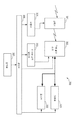
도 2는, 제1 실시형태에 따른 고체 촬상 소자를 나타낸 회로도다.
도 3은, 제1 실시형태에 따른 고체 촬상 소자의 신호 처리부를 나타낸 블록도다.
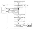
도 4는, 제1 실시형태에 따른 촬상장치를 나타낸 블록도다.
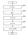
도 5는, 제1 실시형태에 따른 촬상장치에 있어서의 통상 촬영시의 동작을 나타낸 흐름도다.
도 6은, 제1 실시형태에 따른 촬상장치에 있어서의 HDR 촬영시의 동작을 나타낸 흐름도다.
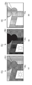
도 7a, 도 7b 및 도 7c는, 제1 실시형태에 따른 촬상장치에 의한 HDR 촬영시에 취득되는 화상의 예를 나타낸 도면이다.
도 8a, 도 8b 및 도 8c는, 제2 실시형태에 따른 촬상장치에 의한 HDR 촬영시에 취득되는 화상의 예를 나타낸 도면이다.
도 9는, 제2 실시형태에 따른 촬상장치에 있어서의 HDR 촬영시의 동작을 나타낸 흐름도다.
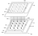
도 10은, 제3 실시형태에 따른 고체 촬상 소자를 도시한 개략도다.
도 11은, 제3 실시형태에 따른 고체 촬상 소자를 나타낸 회로도다.
도 12는, 제3 실시형태에 따른 고체 촬상 소자의 신호 처리부를 나타낸 블록도다.
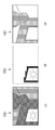
도 13a, 도 13b 및 도 13c는, 제3 실시형태에 따른 촬상장치에 의한 HDR 촬영시에 취득되는 화상의 예를 나타낸 도면이다.
Claims (8)
- 복수의 화소가 배치된 화소부와,
제1 타이밍에서 상기 화소부에서 판독되는 제1 화상신호와, 상기 제1 타이밍과는 다른 제2 타이밍에서 상기 화소부에서 판독되는 제2 화상신호를 합성함으로써, 제3 화상신호를 생성하는 화상신호 합성부와,
상기 제1 화상신호의 신호 레벨을 해석하는 신호 레벨 해석부와,
상기 신호 레벨 해석부에 의한 상기 제1 화상신호의 해석의 결과에 근거하여, 상기 제1 화상신호의 신호 레벨과 상기 제2 화상신호의 신호 레벨을 다르게 하도록 제어하는 제어부를 구비한 고체 촬상 소자.
- 제 1항에 있어서,
상기 화소로부터의 신호에 대해 아날로그-디지털 변환을 행하는 아날로그-디지털 변환부를 더 구비하고,
상기 제1 화상신호 및 상기 제2 화상신호는, 상기 아날로그-디지털 변환부에 의해 아날로그-디지털 변환이 행해진 후의 디지털 화상신호인 고체 촬상 소자.
- 제 1항에 있어서,
상기 제3 화상신호는, 최소의 표현가능한 휘도와 최대의 표현가능한 휘도의 비율이, 상기 제1 화상신호의 비율 및 상기 제2 화상신호의 비율보다 큰 고체 촬상 소자.
- 제 1항에 있어서,
상기 제어부는, 상기 제1 화상신호에 있어서 신호 레벨이 소정의 레벨 이상 및 상기 소정의 레벨 이하 중에서 한개인 상기 화소를 포함하는 영역을, 상기 제2 화상신호를 취득하는 경우에 상기 화소가 판독되는 판독 영역으로서 결정하는 고체 촬상 소자.
- 제 1항에 있어서,
제1 기판과,
상기 제1 기판 위에 배치된 제2 기판을 더 구비하고,
상기 화상신호 합성부는 상기 제1 기판에 배치되고, 상기 화소부는 상기 제2 기판에 배치되어 있는 고체 촬상 소자.
- 제 1항에 있어서,
상기 제어부는, 상기 신호 레벨 해석부에 의한 상기 해석의 결과에 근거하여 상기 제2 화상신호의 신호 레벨을 제어하는 고체 촬상 소자.
- 제 1항에 있어서,
상기 제어부는, 상기 신호 레벨 해석부에 의한 상기 제1 화상신호의 상기 해석의 결과에 근거하여, 상기 제2 화상신호를 취득할 때 판독할 상기 화소를 결정하는 고체 촬상 소자.
- 복수의 화소가 배치된 화소부,
제1 타이밍에서 상기 화소부에서 판독되는 제1 화상신호와, 상기 제1 타이밍과는 다른 제2 타이밍에서 상기 화소부에서 판독되는 제2 화상신호를 합성함으로써, 제3 화상신호를 생성하는 화상신호 합성부,
상기 제1 화상신호의 신호 레벨을 해석하는 신호 레벨 해석부, 및
상기 신호 레벨 해석부에 의한 상기 제1 화상신호의 해석의 결과에 근거하여, 상기 제1 화상신호의 신호 레벨과 상기 제2 화상신호의 신호 레벨을 다르게 하도록 제어하는 제어부를 구비한 고체 촬상 소자와,
복수의 화소가 배치된 화소부와,
상기 고체 촬상 소자에 의해 촬영된 화상을 표시하는 표시부를 구비한 촬상장치.
Applications Claiming Priority (2)
| Application Number | Priority Date | Filing Date | Title |
|---|---|---|---|
| JPJP-P-2015-256094 | 2015-12-28 | ||
| JP2015256094A JP6674255B2 (ja) | 2015-12-28 | 2015-12-28 | 固体撮像素子及び撮像装置 |
Publications (2)
| Publication Number | Publication Date |
|---|---|
| KR20170077784A true KR20170077784A (ko) | 2017-07-06 |
| KR102117858B1 KR102117858B1 (ko) | 2020-06-02 |
Family
ID=59088100
Family Applications (1)
| Application Number | Title | Priority Date | Filing Date |
|---|---|---|---|
| KR1020160165513A Active KR102117858B1 (ko) | 2015-12-28 | 2016-12-07 | 고체 촬상 소자 및 촬상장치 |
Country Status (4)
| Country | Link |
|---|---|
| US (1) | US10122948B2 (ko) |
| JP (1) | JP6674255B2 (ko) |
| KR (1) | KR102117858B1 (ko) |
| CN (1) | CN107071241B (ko) |
Cited By (1)
| Publication number | Priority date | Publication date | Assignee | Title |
|---|---|---|---|---|
| WO2019107769A1 (ko) * | 2017-12-01 | 2019-06-06 | 삼성전자 주식회사 | 이미지 센서의 리드 아웃 속도에 따라 이미지 데이터를 선택적으로 압축하는 전자 장치 및 그의 운용 방법 |
Families Citing this family (2)
| Publication number | Priority date | Publication date | Assignee | Title |
|---|---|---|---|---|
| CN108900789B (zh) * | 2018-08-23 | 2024-07-12 | Oppo广东移动通信有限公司 | 一种图像传感器、摄像头模组及电子设备 |
| JP7374630B2 (ja) | 2019-07-09 | 2023-11-07 | キヤノン株式会社 | 撮像装置及びその駆動方法 |
Citations (5)
| Publication number | Priority date | Publication date | Assignee | Title |
|---|---|---|---|---|
| US20120249728A1 (en) * | 2011-03-31 | 2012-10-04 | Casio Computer Co., Ltd. | Image capturing apparatus for enabling generation of data of panoramic image with wide dynamic range |
| JP2013021660A (ja) * | 2011-07-14 | 2013-01-31 | Sony Corp | 画像処理装置、撮像装置、および画像処理方法、並びにプログラム |
| JP2015144475A (ja) * | 2015-03-11 | 2015-08-06 | キヤノン株式会社 | 撮像装置、撮像装置の制御方法、プログラム及び記憶媒体 |
| US20150244917A1 (en) * | 2014-02-25 | 2015-08-27 | Acer Incorporated | Dynamic exposure adjusting method and electronic apparatus using the same |
| US20150296158A1 (en) * | 2014-04-10 | 2015-10-15 | Forza Silicon Corporation | Reconfigurable CMOS Image Sensor |
Family Cites Families (23)
| Publication number | Priority date | Publication date | Assignee | Title |
|---|---|---|---|---|
| JPH0817455B2 (ja) | 1987-06-09 | 1996-02-21 | キヤノン株式会社 | 撮像装置 |
| JP3166776B2 (ja) * | 1990-11-30 | 2001-05-14 | キヤノン株式会社 | 撮像装置及び撮像方法 |
| JP4996402B2 (ja) * | 2007-09-14 | 2012-08-08 | 株式会社東芝 | 撮像装置 |
| US8115858B2 (en) * | 2008-01-16 | 2012-02-14 | Samsung Electronics Co., Ltd. | System and method for acquiring moving images |
| US7795650B2 (en) * | 2008-12-09 | 2010-09-14 | Teledyne Scientific & Imaging Llc | Method and apparatus for backside illuminated image sensors using capacitively coupled readout integrated circuits |
| US8355059B2 (en) * | 2009-02-06 | 2013-01-15 | Canon Kabushiki Kaisha | Image capturing apparatus and control method thereof |
| KR101614914B1 (ko) * | 2009-07-23 | 2016-04-25 | 삼성전자주식회사 | 모션 적응적 고대비 영상 획득 장치 및 방법 |
| JP5445235B2 (ja) * | 2010-03-09 | 2014-03-19 | ソニー株式会社 | 画像処理装置、画像処理方法およびプログラム |
| US8947555B2 (en) * | 2011-04-18 | 2015-02-03 | Qualcomm Incorporated | White balance optimization with high dynamic range images |
| JP5787648B2 (ja) * | 2011-07-11 | 2015-09-30 | キヤノン株式会社 | 画像処理装置及び画像処理装置の制御方法 |
| US8913153B2 (en) * | 2011-10-06 | 2014-12-16 | Aptina Imaging Corporation | Imaging systems and methods for generating motion-compensated high-dynamic-range images |
| US9185307B2 (en) * | 2012-02-21 | 2015-11-10 | Semiconductor Components Industries, Llc | Detecting transient signals using stacked-chip imaging systems |
| BR112014027066A2 (pt) * | 2012-05-02 | 2017-06-27 | Nikon Corp | dispositivo de formação de imagem |
| JP6137792B2 (ja) * | 2012-07-10 | 2017-05-31 | キヤノン株式会社 | 撮像装置、該撮像装置の制御方法、プログラム、記憶媒体 |
| US20140313316A1 (en) * | 2013-01-30 | 2014-10-23 | SeeScan, Inc. | Adjustable variable resolution inspection systems and methods using multiple image sensors |
| US9686537B2 (en) * | 2013-02-05 | 2017-06-20 | Google Inc. | Noise models for image processing |
| CN104125408B (zh) * | 2013-04-28 | 2018-06-12 | 比亚迪股份有限公司 | 一种高动态范围图像处理方法及装置 |
| KR102106537B1 (ko) * | 2013-09-27 | 2020-05-04 | 삼성전자주식회사 | 하이 다이나믹 레인지 영상 생성 방법 및, 그에 따른 장치, 그에 따른 시스템 |
| US9894287B2 (en) * | 2013-12-06 | 2018-02-13 | Huawei Device (Dongguan) Co., Ltd. | Method and apparatus for acquiring a high dynamic image using multiple cameras |
| US9554506B2 (en) * | 2015-04-27 | 2017-01-31 | Cnh Industrial America Llc | Fluid flow monitoring and control system for an agricultural sprayer |
| CN104869297A (zh) * | 2015-06-15 | 2015-08-26 | 联想(北京)有限公司 | 图像处理方法和电子设备 |
| US9813635B2 (en) * | 2015-08-24 | 2017-11-07 | Motorola Mobility Llc | Method and apparatus for auto exposure value detection for high dynamic range imaging |
| US9544506B1 (en) * | 2015-08-26 | 2017-01-10 | Novatek Microelectronics Corp. | Image processing method for image capturing device |
-
2015
- 2015-12-28 JP JP2015256094A patent/JP6674255B2/ja active Active
-
2016
- 2016-12-07 KR KR1020160165513A patent/KR102117858B1/ko active Active
- 2016-12-16 US US15/381,840 patent/US10122948B2/en active Active
- 2016-12-28 CN CN201611236982.XA patent/CN107071241B/zh active Active
Patent Citations (5)
| Publication number | Priority date | Publication date | Assignee | Title |
|---|---|---|---|---|
| US20120249728A1 (en) * | 2011-03-31 | 2012-10-04 | Casio Computer Co., Ltd. | Image capturing apparatus for enabling generation of data of panoramic image with wide dynamic range |
| JP2013021660A (ja) * | 2011-07-14 | 2013-01-31 | Sony Corp | 画像処理装置、撮像装置、および画像処理方法、並びにプログラム |
| US20150244917A1 (en) * | 2014-02-25 | 2015-08-27 | Acer Incorporated | Dynamic exposure adjusting method and electronic apparatus using the same |
| US20150296158A1 (en) * | 2014-04-10 | 2015-10-15 | Forza Silicon Corporation | Reconfigurable CMOS Image Sensor |
| JP2015144475A (ja) * | 2015-03-11 | 2015-08-06 | キヤノン株式会社 | 撮像装置、撮像装置の制御方法、プログラム及び記憶媒体 |
Cited By (3)
| Publication number | Priority date | Publication date | Assignee | Title |
|---|---|---|---|---|
| WO2019107769A1 (ko) * | 2017-12-01 | 2019-06-06 | 삼성전자 주식회사 | 이미지 센서의 리드 아웃 속도에 따라 이미지 데이터를 선택적으로 압축하는 전자 장치 및 그의 운용 방법 |
| KR20190065096A (ko) * | 2017-12-01 | 2019-06-11 | 삼성전자주식회사 | 이미지 합성 방법 및 장치 |
| US11115605B2 (en) | 2017-12-01 | 2021-09-07 | Samsung Electronics Co., Ltd. | Electronic device for selectively compressing image data according to read out speed of image sensor, and method for operating same |
Also Published As
| Publication number | Publication date |
|---|---|
| US10122948B2 (en) | 2018-11-06 |
| CN107071241A (zh) | 2017-08-18 |
| JP6674255B2 (ja) | 2020-04-01 |
| US20170187971A1 (en) | 2017-06-29 |
| JP2017120971A (ja) | 2017-07-06 |
| KR102117858B1 (ko) | 2020-06-02 |
| CN107071241B (zh) | 2020-06-23 |
Similar Documents
| Publication | Publication Date | Title |
|---|---|---|
| JP6222908B2 (ja) | 画像処理装置、方法およびプログラム、並びに画像処理装置を有する撮像装置 | |
| JP4448888B2 (ja) | 撮像装置及び撮像装置の信号処理方法 | |
| US9571742B2 (en) | Image capture apparatus and control method thereof | |
| CN105282431B (zh) | 摄像装置及摄像装置的控制方法 | |
| JP5946421B2 (ja) | 撮像装置及びその制御方法 | |
| US10638072B2 (en) | Control apparatus, image pickup apparatus, and control method for performing noise correction of imaging signal | |
| US9948850B2 (en) | Image sensor, control method for the same, and image capture apparatus | |
| US20140118587A1 (en) | Image pickup apparatus and driving method therefor | |
| EP3565238A1 (en) | Imaging device, camera and imaging method | |
| US10033951B2 (en) | Image sensor that performs different readout operations and image capturing apparatus including image sensor | |
| JP2010062638A (ja) | 撮像装置 | |
| CN105100601A (zh) | 摄像装置及其控制方法和信号处理装置 | |
| JP2017216647A (ja) | 撮像素子、撮像装置、および撮像信号処理方法 | |
| US10225494B2 (en) | Image capturing apparatus and control method thereof | |
| JP5701942B2 (ja) | 撮像装置、カメラシステム及び画像処理方法 | |
| KR102117858B1 (ko) | 고체 촬상 소자 및 촬상장치 | |
| US10203206B2 (en) | Image capture apparatus having signal readouts using distance measurement region | |
| JP2022111738A (ja) | 撮像装置および画像処理方法 | |
| JP2014107739A (ja) | 撮像装置及びその制御方法 | |
| JP2013145985A (ja) | 撮像装置、その制御方法及び撮像システム | |
| JP6723709B2 (ja) | 撮像装置、画像処理装置及びそれらの制御方法 | |
| JP6167473B2 (ja) | 撮像装置 | |
| JP7020463B2 (ja) | 撮像装置 | |
| JP5408029B2 (ja) | デジタルカメラ | |
| JP6883082B2 (ja) | 撮像装置及びその制御方法 |
Legal Events
| Date | Code | Title | Description |
|---|---|---|---|
| PA0109 | Patent application |
Patent event code: PA01091R01D Comment text: Patent Application Patent event date: 20161207 |
|
| PG1501 | Laying open of application | ||
| A201 | Request for examination | ||
| PA0201 | Request for examination |
Patent event code: PA02012R01D Patent event date: 20180607 Comment text: Request for Examination of Application Patent event code: PA02011R01I Patent event date: 20161207 Comment text: Patent Application |
|
| E902 | Notification of reason for refusal | ||
| PE0902 | Notice of grounds for rejection |
Comment text: Notification of reason for refusal Patent event date: 20190829 Patent event code: PE09021S01D |
|
| E701 | Decision to grant or registration of patent right | ||
| PE0701 | Decision of registration |
Patent event code: PE07011S01D Comment text: Decision to Grant Registration Patent event date: 20200304 |
|
| GRNT | Written decision to grant | ||
| PR0701 | Registration of establishment |
Comment text: Registration of Establishment Patent event date: 20200527 Patent event code: PR07011E01D |
|
| PR1002 | Payment of registration fee |
Payment date: 20200528 End annual number: 3 Start annual number: 1 |
|
| PG1601 | Publication of registration |