KR20170078457A - 와이어 실리콘 고무가 콘택 핀과 반도체 기기 사이에 인터포저 되는 번인 테스트 소켓 - Google Patents
와이어 실리콘 고무가 콘택 핀과 반도체 기기 사이에 인터포저 되는 번인 테스트 소켓 Download PDFInfo
- Publication number
- KR20170078457A KR20170078457A KR1020150188990A KR20150188990A KR20170078457A KR 20170078457 A KR20170078457 A KR 20170078457A KR 1020150188990 A KR1020150188990 A KR 1020150188990A KR 20150188990 A KR20150188990 A KR 20150188990A KR 20170078457 A KR20170078457 A KR 20170078457A
- Authority
- KR
- South Korea
- Prior art keywords
- semiconductor device
- contact
- bump
- pin
- wire
- Prior art date
- Legal status (The legal status is an assumption and is not a legal conclusion. Google has not performed a legal analysis and makes no representation as to the accuracy of the status listed.)
- Granted
Links
- 239000004065 semiconductor Substances 0.000 title claims abstract description 53
- 229920002379 silicone rubber Polymers 0.000 title claims abstract description 37
- 238000012360 testing method Methods 0.000 title claims abstract description 37
- 239000004945 silicone rubber Substances 0.000 claims abstract description 32
- 238000000034 method Methods 0.000 claims description 12
- 238000003825 pressing Methods 0.000 claims description 3
- 238000007689 inspection Methods 0.000 description 7
- PXHVJJICTQNCMI-UHFFFAOYSA-N Nickel Chemical compound [Ni] PXHVJJICTQNCMI-UHFFFAOYSA-N 0.000 description 5
- 229920001971 elastomer Polymers 0.000 description 5
- 239000005060 rubber Substances 0.000 description 5
- 239000010949 copper Substances 0.000 description 4
- 239000002245 particle Substances 0.000 description 3
- 230000003252 repetitive effect Effects 0.000 description 3
- 238000005476 soldering Methods 0.000 description 3
- RYGMFSIKBFXOCR-UHFFFAOYSA-N Copper Chemical compound [Cu] RYGMFSIKBFXOCR-UHFFFAOYSA-N 0.000 description 2
- XEEYBQQBJWHFJM-UHFFFAOYSA-N Iron Chemical compound [Fe] XEEYBQQBJWHFJM-UHFFFAOYSA-N 0.000 description 2
- 239000000853 adhesive Substances 0.000 description 2
- 230000001070 adhesive effect Effects 0.000 description 2
- 229910052802 copper Inorganic materials 0.000 description 2
- 230000007423 decrease Effects 0.000 description 2
- PCHJSUWPFVWCPO-UHFFFAOYSA-N gold Chemical compound [Au] PCHJSUWPFVWCPO-UHFFFAOYSA-N 0.000 description 2
- 239000010931 gold Substances 0.000 description 2
- 229910052737 gold Inorganic materials 0.000 description 2
- 238000004519 manufacturing process Methods 0.000 description 2
- 229910052759 nickel Inorganic materials 0.000 description 2
- 239000004593 Epoxy Substances 0.000 description 1
- 244000043261 Hevea brasiliensis Species 0.000 description 1
- 229920006311 Urethane elastomer Polymers 0.000 description 1
- 229910045601 alloy Inorganic materials 0.000 description 1
- 239000000956 alloy Substances 0.000 description 1
- 229910017052 cobalt Inorganic materials 0.000 description 1
- 239000010941 cobalt Substances 0.000 description 1
- GUTLYIVDDKVIGB-UHFFFAOYSA-N cobalt atom Chemical compound [Co] GUTLYIVDDKVIGB-UHFFFAOYSA-N 0.000 description 1
- 239000004020 conductor Substances 0.000 description 1
- 238000010586 diagram Methods 0.000 description 1
- 230000000694 effects Effects 0.000 description 1
- 239000003822 epoxy resin Substances 0.000 description 1
- 239000000945 filler Substances 0.000 description 1
- 229910052742 iron Inorganic materials 0.000 description 1
- 239000007788 liquid Substances 0.000 description 1
- 239000002184 metal Substances 0.000 description 1
- 229910052751 metal Inorganic materials 0.000 description 1
- 238000012986 modification Methods 0.000 description 1
- 230000004048 modification Effects 0.000 description 1
- 229920003052 natural elastomer Polymers 0.000 description 1
- 229920001194 natural rubber Polymers 0.000 description 1
- 239000005011 phenolic resin Substances 0.000 description 1
- 229920002857 polybutadiene Polymers 0.000 description 1
- 229920001721 polyimide Polymers 0.000 description 1
- 229920001195 polyisoprene Polymers 0.000 description 1
- 239000002861 polymer material Substances 0.000 description 1
- 229920001296 polysiloxane Polymers 0.000 description 1
Images




Classifications
-
- G—PHYSICS
- G01—MEASURING; TESTING
- G01R—MEASURING ELECTRIC VARIABLES; MEASURING MAGNETIC VARIABLES
- G01R1/00—Details of instruments or arrangements of the types included in groups G01R5/00 - G01R13/00 and G01R31/00
- G01R1/02—General constructional details
- G01R1/04—Housings; Supporting members; Arrangements of terminals
- G01R1/0408—Test fixtures or contact fields; Connectors or connecting adaptors; Test clips; Test sockets
- G01R1/0433—Sockets for IC's or transistors
- G01R1/0441—Details
- G01R1/0466—Details concerning contact pieces or mechanical details, e.g. hinges or cams; Shielding
-
- G—PHYSICS
- G01—MEASURING; TESTING
- G01R—MEASURING ELECTRIC VARIABLES; MEASURING MAGNETIC VARIABLES
- G01R1/00—Details of instruments or arrangements of the types included in groups G01R5/00 - G01R13/00 and G01R31/00
- G01R1/02—General constructional details
- G01R1/06—Measuring leads; Measuring probes
- G01R1/067—Measuring probes
- G01R1/073—Multiple probes
- G01R1/07307—Multiple probes with individual probe elements, e.g. needles, cantilever beams or bump contacts, fixed in relation to each other, e.g. bed of nails fixture or probe card
- G01R1/0735—Multiple probes with individual probe elements, e.g. needles, cantilever beams or bump contacts, fixed in relation to each other, e.g. bed of nails fixture or probe card arranged on a flexible frame or film
-
- G—PHYSICS
- G01—MEASURING; TESTING
- G01R—MEASURING ELECTRIC VARIABLES; MEASURING MAGNETIC VARIABLES
- G01R31/00—Arrangements for testing electric properties; Arrangements for locating electric faults; Arrangements for electrical testing characterised by what is being tested not provided for elsewhere
- G01R31/28—Testing of electronic circuits, e.g. by signal tracer
- G01R31/2851—Testing of integrated circuits [IC]
- G01R31/2855—Environmental, reliability or burn-in testing
- G01R31/286—External aspects, e.g. related to chambers, contacting devices or handlers
- G01R31/2863—Contacting devices, e.g. sockets, burn-in boards or mounting fixtures
-
- G—PHYSICS
- G01—MEASURING; TESTING
- G01R—MEASURING ELECTRIC VARIABLES; MEASURING MAGNETIC VARIABLES
- G01R31/00—Arrangements for testing electric properties; Arrangements for locating electric faults; Arrangements for electrical testing characterised by what is being tested not provided for elsewhere
- G01R31/28—Testing of electronic circuits, e.g. by signal tracer
- G01R31/2851—Testing of integrated circuits [IC]
- G01R31/2886—Features relating to contacting the IC under test, e.g. probe heads; chucks
- G01R31/2887—Features relating to contacting the IC under test, e.g. probe heads; chucks involving moving the probe head or the IC under test; docking stations
-
- G—PHYSICS
- G01—MEASURING; TESTING
- G01R—MEASURING ELECTRIC VARIABLES; MEASURING MAGNETIC VARIABLES
- G01R31/00—Arrangements for testing electric properties; Arrangements for locating electric faults; Arrangements for electrical testing characterised by what is being tested not provided for elsewhere
- G01R31/28—Testing of electronic circuits, e.g. by signal tracer
- G01R31/2851—Testing of integrated circuits [IC]
- G01R31/2886—Features relating to contacting the IC under test, e.g. probe heads; chucks
- G01R31/2889—Interfaces, e.g. between probe and tester
Landscapes
- Engineering & Computer Science (AREA)
- Physics & Mathematics (AREA)
- General Physics & Mathematics (AREA)
- Computer Hardware Design (AREA)
- Microelectronics & Electronic Packaging (AREA)
- General Engineering & Computer Science (AREA)
- Environmental & Geological Engineering (AREA)
- Testing Of Individual Semiconductor Devices (AREA)
Abstract
Description
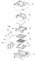
도 2 내지 도 4는 본 발명에 의한 와이어 실리콘 고무가 콘택 핀가 반도체 기기 사이에서 인터포저 되는 번인 테스트 소켓의 구성을 각각 나타내는 사시도, 분해 사시도, 및 부분 절개 사시도.
도 5는 본 발명에 의한 와이어 실리콘 고무가 콘택 핀과 반도체 기기 사이에서 인터포저 되어 번인 테스트 되는 과정을 나타내는 단면도.
120: 핀 플레이트 122: 콘택 핀
130: 슬라이드 140: 와이어 실리콘 고무
150: 가이드 160: 래치
170: 커버
Claims (10)
- 테스트 장치와 결합되는 베이스;
상기 베이스에 탑재되고 한 쌍의 탄성 집게(nipper) 타입의 콘택 핀을 다수 수용하는 핀 플레이트;
하부 범프를 통하여 상기 콘택 핀과 연결되고, 상부 범프를 통하여 반도체 기기의 접속 단자와 연결되는 와이어 실리콘 고무;
하부에서는 상기 와이어 실리콘 고무를 상기 베이스에 고정하면서 상부에서는 상기 반도체 기기를 안내하는 가이드;
상기 베이스에 설치되어 상기 반도체 기기의 유동을 방지하는 한 쌍의 래치; 및
상기 가이드 상부의 상기 베이스에 설치되어, 상기 래치의 구동력을 제공하는 커버를 포함하여 구성됨을 특징으로 하는 번인 테스트 소켓. - 제 1 항에 있어서,
상하 왕복 이동을 통하여 상기 집게를 가압하거나 복원하는 슬라이드를 더 포함하여 구성됨을 특징으로 하는 번인 테스트 소켓. - 제 2 항에 있어서,
상기 집게를 가압하는 경우 상기 슬라이드는 상기 와이어 실리콘 고무의 저면과 접촉한 상태로 유지되고, 상기 집게를 복원하는 경우 상기 슬라이드는 상기 핀 플레이트 상면과 접촉한 상태로 유지되는 것을 특징으로 하는 번인 테스트 소켓. - 제 2 항에 있어서,
상기 콘택 핀은,
상기 테스트 보드의 접속 단자에 체결되고 상기 핀 플레이트에 고정 결합되는 핀 바디;
상기 슬라이드에 의하여 가압 및 복원되는 핀 스프링; 및
상기 반도체 기기의 접속 단자와 체결되는 핀 헤드를 포함하여 구성됨을 특징으로 하는 번인 테스트 소켓. - 제 4 항에 있어서,
상기 핀 헤드는 상기 하부 범프와 접촉 분리되는 한 쌍의 접촉 팁을 포함하고, 일방 접촉 팁에 볼록 요철 처리되고, 타방 접촉 팁에 오목 요철 처리되는 것을 특징으로 하는 번인 테스트 소켓. - 제 5 항에 있어서,
상기 하부 범프 및 상기 상부 범프는 와이어 본딩에 의하여 형성되는 스터드 범프로 구성되고, 상기 하부 범프의 스터드는 상기 상부 범프의 스터드보다 긴 것을 특징으로 하는 번인 테스트 소켓. - 제 6 항에 있어서,
상기 하부 범프는 상기 스터드의 길이가 상기 접촉 팁의 길이보다 길게 연장되는 것을 특징으로 하는 번인 테스트 소켓. - 콘택 핀이 하부에서 테스트 장치의 접속 단자와 결합되고, 상부에서 반도체 기기의 접속 단자와 결합되어 반도체 기기의 전기적 특성을 검사 하는 번인 테스트 소켓에 있어서,
상기 콘택 핀과 상기 반도체 기기 사이에서 인터포저 되는 와이어 실리콘 고무를 더 포함하고,
상기 와이어 실리콘 고무는,
다수 제1패드가 형성되는 제1PCB 필름,
상기 제1패드의 제1표면에 와이어 본딩 되는 도전 와이어;
상기 제1PCB 필름 상에 설치되고 상기 도전 와이어를 지지하는 절연 실리콘 고무; 및
상기 절연 실리콘 고무 상에 설치되고 다수 제2패드의 제1표면에 상기 도전 와이어가 연결되는 제2PCB 필름을 포함하여 구성됨을 특징으로 하는 번인 테스트 소켓. - 제 8 항에 있어서,
상기 제1패드는 제2표면에 하부 스터드 범프를 통하여 상기 콘택 핀과 접속되고,
상기 제2패드는 제2표면에 상부 스터드 범프를 통하여 상기 반도체 기기의 도전 볼과 접속되는 것을 특징으로 하는 번인 테스트 소켓. - 제 9 항에 있어서,
상기 하부 스터드 범프를 형성할 때 본딩 넥을 길게 처리하여 스터드의 길이가 상기 상부 범프보다 긴 것을 특징으로 하는 번인 테스트 소켓.
Priority Applications (1)
| Application Number | Priority Date | Filing Date | Title |
|---|---|---|---|
| KR1020150188990A KR101806472B1 (ko) | 2015-12-29 | 2015-12-29 | 와이어 실리콘 고무가 콘택 핀과 반도체 기기 사이에 인터포저 되는 번인 테스트 소켓 |
Applications Claiming Priority (1)
| Application Number | Priority Date | Filing Date | Title |
|---|---|---|---|
| KR1020150188990A KR101806472B1 (ko) | 2015-12-29 | 2015-12-29 | 와이어 실리콘 고무가 콘택 핀과 반도체 기기 사이에 인터포저 되는 번인 테스트 소켓 |
Publications (2)
| Publication Number | Publication Date |
|---|---|
| KR20170078457A true KR20170078457A (ko) | 2017-07-07 |
| KR101806472B1 KR101806472B1 (ko) | 2017-12-07 |
Family
ID=59353788
Family Applications (1)
| Application Number | Title | Priority Date | Filing Date |
|---|---|---|---|
| KR1020150188990A Active KR101806472B1 (ko) | 2015-12-29 | 2015-12-29 | 와이어 실리콘 고무가 콘택 핀과 반도체 기기 사이에 인터포저 되는 번인 테스트 소켓 |
Country Status (1)
| Country | Link |
|---|---|
| KR (1) | KR101806472B1 (ko) |
Cited By (9)
| Publication number | Priority date | Publication date | Assignee | Title |
|---|---|---|---|---|
| CN109342912A (zh) * | 2018-09-30 | 2019-02-15 | 西安微电子技术研究所 | Smd表贴封装器件老炼的工装夹具 |
| KR102029400B1 (ko) * | 2018-04-27 | 2019-10-07 | 주식회사 마이크로컨텍솔루션 | 반도체 칩 테스트 소켓 |
| KR102036105B1 (ko) * | 2018-11-06 | 2019-10-24 | (주)티에스이 | 신호 전송 커넥터 |
| KR102105874B1 (ko) * | 2019-02-21 | 2020-04-29 | 주식회사 티에프이 | 반도체패키지 테스트용 소켓모듈 및 그를 구비하는 반도체패키지 도킹플레이트 |
| KR102210651B1 (ko) * | 2020-04-16 | 2021-02-02 | 캠아이티(주) | 후크 체결형 반도체 테스트 소켓 |
| KR102213076B1 (ko) * | 2020-01-07 | 2021-02-08 | (주)마이크로컨텍솔루션 | 반도체 칩 패키지 테스트 소켓 |
| KR20220091171A (ko) * | 2020-12-23 | 2022-06-30 | (주)마이크로컨텍솔루션 | 반도체 칩 테스트 소켓 |
| KR20240059117A (ko) * | 2022-10-27 | 2024-05-07 | 주식회사 오킨스전자 | 테스트 소켓의 측면 열방출 장치 |
| KR102746761B1 (ko) * | 2023-07-19 | 2024-12-26 | 모아테크(주) | 반도체 lga 번인 테스트소켓의 부분절연코팅공정 |
Families Citing this family (1)
| Publication number | Priority date | Publication date | Assignee | Title |
|---|---|---|---|---|
| KR102726429B1 (ko) * | 2021-12-08 | 2024-11-05 | (주)마이크로컨텍솔루션 | 테스트 소켓 |
Family Cites Families (3)
| Publication number | Priority date | Publication date | Assignee | Title |
|---|---|---|---|---|
| KR200299600Y1 (ko) * | 2002-10-07 | 2002-12-31 | 주식회사 오킨스전자 | 비지에이형 집적회로 패키지용 소켓 |
| US7118389B2 (en) * | 2004-06-18 | 2006-10-10 | Palo Alto Research Center Incorporated | Stud bump socket |
| KR200446269Y1 (ko) * | 2008-02-25 | 2009-10-29 | 주식회사 아이에스시테크놀러지 | 갭부재를 가진 테스트소켓 |
-
2015
- 2015-12-29 KR KR1020150188990A patent/KR101806472B1/ko active Active
Cited By (9)
| Publication number | Priority date | Publication date | Assignee | Title |
|---|---|---|---|---|
| KR102029400B1 (ko) * | 2018-04-27 | 2019-10-07 | 주식회사 마이크로컨텍솔루션 | 반도체 칩 테스트 소켓 |
| CN109342912A (zh) * | 2018-09-30 | 2019-02-15 | 西安微电子技术研究所 | Smd表贴封装器件老炼的工装夹具 |
| KR102036105B1 (ko) * | 2018-11-06 | 2019-10-24 | (주)티에스이 | 신호 전송 커넥터 |
| KR102105874B1 (ko) * | 2019-02-21 | 2020-04-29 | 주식회사 티에프이 | 반도체패키지 테스트용 소켓모듈 및 그를 구비하는 반도체패키지 도킹플레이트 |
| KR102213076B1 (ko) * | 2020-01-07 | 2021-02-08 | (주)마이크로컨텍솔루션 | 반도체 칩 패키지 테스트 소켓 |
| KR102210651B1 (ko) * | 2020-04-16 | 2021-02-02 | 캠아이티(주) | 후크 체결형 반도체 테스트 소켓 |
| KR20220091171A (ko) * | 2020-12-23 | 2022-06-30 | (주)마이크로컨텍솔루션 | 반도체 칩 테스트 소켓 |
| KR20240059117A (ko) * | 2022-10-27 | 2024-05-07 | 주식회사 오킨스전자 | 테스트 소켓의 측면 열방출 장치 |
| KR102746761B1 (ko) * | 2023-07-19 | 2024-12-26 | 모아테크(주) | 반도체 lga 번인 테스트소켓의 부분절연코팅공정 |
Also Published As
| Publication number | Publication date |
|---|---|
| KR101806472B1 (ko) | 2017-12-07 |
Similar Documents
| Publication | Publication Date | Title |
|---|---|---|
| KR101806472B1 (ko) | 와이어 실리콘 고무가 콘택 핀과 반도체 기기 사이에 인터포저 되는 번인 테스트 소켓 | |
| KR101482911B1 (ko) | 탄성체 에스 컨택터를 가지는 반도체 디바이스 테스트용 소켓 | |
| KR101493898B1 (ko) | 반도체 테스트 장치의 컨택터 | |
| KR101833009B1 (ko) | 도전성 파티클이 자화된 도전 와이어에 의하여 자성 배열되는 테스트 소켓 및 그 제조 방법 | |
| KR101353481B1 (ko) | 고밀도 도전부를 가지는 테스트용 소켓 | |
| KR101366171B1 (ko) | 고밀도 도전부를 가지는 테스트용 소켓 | |
| KR101737047B1 (ko) | 메탈 코어 솔더 볼을 이용하는 도전 와이어 본딩 구조체 및 그 제조방법, 그리고 이를 포함하는 테스트 소켓 | |
| KR101471116B1 (ko) | 고밀도 도전부를 가지는 테스트용 소켓 | |
| KR102271503B1 (ko) | 신호 전송 커넥터 | |
| US9653833B2 (en) | Contact pin and electrical component socket | |
| KR102410156B1 (ko) | 반도체 패키지의 테스트 장치 | |
| TWI900344B (zh) | 用於測試半導體封裝的測試插座和設備 | |
| KR20190052726A (ko) | 양방향 도전성 모듈 | |
| KR102887593B1 (ko) | 포고 핀 및 이를 포함하는 테스트 소켓 | |
| KR101683018B1 (ko) | 러버 콘택의 테스트 보드, 및 이를 포함하는 번인 테스트 소켓 | |
| KR101173191B1 (ko) | 테스트 소켓 | |
| KR101694507B1 (ko) | 와이어마다 개별 도전 실리콘 고무에 의하여 가압 전도되는 테스트 소켓 | |
| KR101708487B1 (ko) | 도전 실리콘 고무 안에 더블 도전 와이어를 포함하는 테스트 소켓, 및 그 제조 방법 | |
| KR102728126B1 (ko) | 스트로크 조절수단을 구비한 테스트 소켓 | |
| KR101800812B1 (ko) | 실리콘 고무에 관통 홀을 포함하는 테스트 소켓, 및 그 제조 방법 | |
| KR20190033842A (ko) | 강자성체 및 메탈 파우더의 하이브리드 콘택 테스트 소켓 | |
| KR101678366B1 (ko) | 컨택터 제조방법 | |
| KR101802426B1 (ko) | 와이어 실리콘 보드에 의하여 mems 필름의 콘택 특성이 개선되는 하이브리드 테스트 소켓 | |
| KR102270275B1 (ko) | 테스트 소켓 | |
| KR102714657B1 (ko) | 테스트 소켓 |
Legal Events
| Date | Code | Title | Description |
|---|---|---|---|
| A201 | Request for examination | ||
| PA0109 | Patent application |
Patent event code: PA01091R01D Comment text: Patent Application Patent event date: 20151229 |
|
| PA0201 | Request for examination | ||
| E902 | Notification of reason for refusal | ||
| PE0902 | Notice of grounds for rejection |
Comment text: Notification of reason for refusal Patent event date: 20170403 Patent event code: PE09021S01D |
|
| PG1501 | Laying open of application | ||
| E90F | Notification of reason for final refusal | ||
| PE0902 | Notice of grounds for rejection |
Comment text: Final Notice of Reason for Refusal Patent event date: 20170818 Patent event code: PE09021S02D |
|
| E701 | Decision to grant or registration of patent right | ||
| PE0701 | Decision of registration |
Patent event code: PE07011S01D Comment text: Decision to Grant Registration Patent event date: 20170901 |
|
| GRNT | Written decision to grant | ||
| PR0701 | Registration of establishment |
Comment text: Registration of Establishment Patent event date: 20171201 Patent event code: PR07011E01D |
|
| PR1002 | Payment of registration fee |
Payment date: 20171204 End annual number: 3 Start annual number: 1 |
|
| PG1601 | Publication of registration | ||
| PR1001 | Payment of annual fee |
Payment date: 20211201 Start annual number: 5 End annual number: 5 |
|
| PR1001 | Payment of annual fee |
Payment date: 20231130 Start annual number: 7 End annual number: 7 |
|
| PR1001 | Payment of annual fee |
Payment date: 20241202 Start annual number: 8 End annual number: 8 |