KR20170083384A - 반도체 웨이퍼, 반도체 구조체 및 이를 제조하는 방법 - Google Patents
반도체 웨이퍼, 반도체 구조체 및 이를 제조하는 방법 Download PDFInfo
- Publication number
- KR20170083384A KR20170083384A KR1020160002779A KR20160002779A KR20170083384A KR 20170083384 A KR20170083384 A KR 20170083384A KR 1020160002779 A KR1020160002779 A KR 1020160002779A KR 20160002779 A KR20160002779 A KR 20160002779A KR 20170083384 A KR20170083384 A KR 20170083384A
- Authority
- KR
- South Korea
- Prior art keywords
- semiconductor wafer
- height
- inclined surface
- wafer
- point
- Prior art date
- Legal status (The legal status is an assumption and is not a legal conclusion. Google has not performed a legal analysis and makes no representation as to the accuracy of the status listed.)
- Granted
Links
Images


Classifications
-
- H01L23/544—
-
- H—ELECTRICITY
- H10—SEMICONDUCTOR DEVICES; ELECTRIC SOLID-STATE DEVICES NOT OTHERWISE PROVIDED FOR
- H10W—GENERIC PACKAGES, INTERCONNECTIONS, CONNECTORS OR OTHER CONSTRUCTIONAL DETAILS OF DEVICES COVERED BY CLASS H10
- H10W42/00—Arrangements for protection of devices
- H10W42/121—Arrangements for protection of devices protecting against mechanical damage
-
- H01L21/324—
-
- H01L21/682—
-
- H01L22/12—
-
- H—ELECTRICITY
- H10—SEMICONDUCTOR DEVICES; ELECTRIC SOLID-STATE DEVICES NOT OTHERWISE PROVIDED FOR
- H10P—GENERIC PROCESSES OR APPARATUS FOR THE MANUFACTURE OR TREATMENT OF DEVICES COVERED BY CLASS H10
- H10P14/00—Formation of materials, e.g. in the shape of layers or pillars
- H10P14/20—Formation of materials, e.g. in the shape of layers or pillars of semiconductor materials
- H10P14/24—Formation of materials, e.g. in the shape of layers or pillars of semiconductor materials using chemical vapour deposition [CVD]
-
- H—ELECTRICITY
- H10—SEMICONDUCTOR DEVICES; ELECTRIC SOLID-STATE DEVICES NOT OTHERWISE PROVIDED FOR
- H10P—GENERIC PROCESSES OR APPARATUS FOR THE MANUFACTURE OR TREATMENT OF DEVICES COVERED BY CLASS H10
- H10P74/00—Testing or measuring during manufacture or treatment of wafers, substrates or devices
- H10P74/20—Testing or measuring during manufacture or treatment of wafers, substrates or devices characterised by the properties tested or measured, e.g. structural or electrical properties
- H10P74/203—Structural properties, e.g. testing or measuring thicknesses, line widths, warpage, bond strengths or physical defects
-
- H—ELECTRICITY
- H10—SEMICONDUCTOR DEVICES; ELECTRIC SOLID-STATE DEVICES NOT OTHERWISE PROVIDED FOR
- H10P—GENERIC PROCESSES OR APPARATUS FOR THE MANUFACTURE OR TREATMENT OF DEVICES COVERED BY CLASS H10
- H10P90/00—Preparation of wafers not covered by a single main group of this subclass, e.g. wafer reinforcement
- H10P90/12—Preparing bulk and homogeneous wafers
- H10P90/123—Preparing bulk and homogeneous wafers by grinding or lapping
-
- H—ELECTRICITY
- H10—SEMICONDUCTOR DEVICES; ELECTRIC SOLID-STATE DEVICES NOT OTHERWISE PROVIDED FOR
- H10P—GENERIC PROCESSES OR APPARATUS FOR THE MANUFACTURE OR TREATMENT OF DEVICES COVERED BY CLASS H10
- H10P90/00—Preparation of wafers not covered by a single main group of this subclass, e.g. wafer reinforcement
- H10P90/12—Preparing bulk and homogeneous wafers
- H10P90/128—Preparing bulk and homogeneous wafers by edge treatment, e.g. chamfering
-
- H—ELECTRICITY
- H10—SEMICONDUCTOR DEVICES; ELECTRIC SOLID-STATE DEVICES NOT OTHERWISE PROVIDED FOR
- H10P—GENERIC PROCESSES OR APPARATUS FOR THE MANUFACTURE OR TREATMENT OF DEVICES COVERED BY CLASS H10
- H10P90/00—Preparation of wafers not covered by a single main group of this subclass, e.g. wafer reinforcement
- H10P90/12—Preparing bulk and homogeneous wafers
- H10P90/18—Preparing bulk and homogeneous wafers by shaping
-
- H—ELECTRICITY
- H10—SEMICONDUCTOR DEVICES; ELECTRIC SOLID-STATE DEVICES NOT OTHERWISE PROVIDED FOR
- H10P—GENERIC PROCESSES OR APPARATUS FOR THE MANUFACTURE OR TREATMENT OF DEVICES COVERED BY CLASS H10
- H10P95/00—Generic processes or apparatus for manufacture or treatments not covered by the other groups of this subclass
- H10P95/90—Thermal treatments, e.g. annealing or sintering
-
- H—ELECTRICITY
- H10—SEMICONDUCTOR DEVICES; ELECTRIC SOLID-STATE DEVICES NOT OTHERWISE PROVIDED FOR
- H10W—GENERIC PACKAGES, INTERCONNECTIONS, CONNECTORS OR OTHER CONSTRUCTIONAL DETAILS OF DEVICES COVERED BY CLASS H10
- H10W46/00—Marks applied to devices, e.g. for alignment or identification
-
- H01L2223/54493—
-
- H—ELECTRICITY
- H10—SEMICONDUCTOR DEVICES; ELECTRIC SOLID-STATE DEVICES NOT OTHERWISE PROVIDED FOR
- H10W—GENERIC PACKAGES, INTERCONNECTIONS, CONNECTORS OR OTHER CONSTRUCTIONAL DETAILS OF DEVICES COVERED BY CLASS H10
- H10W46/00—Marks applied to devices, e.g. for alignment or identification
- H10W46/201—Marks applied to devices, e.g. for alignment or identification located on the periphery of wafers, e.g. orientation notches or lot numbers
-
- H—ELECTRICITY
- H10—SEMICONDUCTOR DEVICES; ELECTRIC SOLID-STATE DEVICES NOT OTHERWISE PROVIDED FOR
- H10W—GENERIC PACKAGES, INTERCONNECTIONS, CONNECTORS OR OTHER CONSTRUCTIONAL DETAILS OF DEVICES COVERED BY CLASS H10
- H10W46/00—Marks applied to devices, e.g. for alignment or identification
- H10W46/301—Marks applied to devices, e.g. for alignment or identification for alignment
Landscapes
- Mechanical Treatment Of Semiconductor (AREA)
- Grinding And Polishing Of Tertiary Curved Surfaces And Surfaces With Complex Shapes (AREA)
- Container, Conveyance, Adherence, Positioning, Of Wafer (AREA)
Abstract
Description
도 2는 도 1의 Ⅱ-Ⅱ′선에 따른 반도체 웨이퍼를 절단하여 나타내는 단면도이다.
도 3은 도 1의 Ⅲ-Ⅲ′선에 따른 반도체 웨이퍼를 절단하여 나타내는 단면도이다.
도 4는 본 발명의 기술적 사상의 일 실시예에 따른 반도체 구조체의 평면도이다.
도 5는 본 발명의 기술적 사상의 일 실시예에 따른 반도체 웨이퍼의 제조 방법을 나타내는 흐름도이다.
도 6은 본 발명의 기술적 사상의 일 실시예에 따른 반도체 웨이퍼의 제조 방법을 나타내는 흐름도이다.
도 7은 본 발명의 기술적 사상의 일 실시예에 따른 반도체 웨이퍼의 제조 방법을 나타내는 흐름도이다.
도 8은 본 발명의 기술적 사상의 일 실시예에 따른 반도체 소자를 제조하는 방법을 나타내는 흐름도이다.
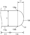
111: 칩 형성 영역 113: 가장자리 영역
120: 노치부 121: 개구
130: 제1 베벨부 131: 제1 경사면
140: 제2 베벨부 141: 제2 경사면
200: 반도체 구조체 210: 반도체 칩들
Claims (10)
- 서로 반대되는 제1 면과 제2 면을 가지고, 그 외주로부터 중심부를 향하여 형성된 개구를 구비한 노치부를 포함하는 반도체 웨이퍼를 준비하는 단계;
상기 반도체 웨이퍼의 외주를 가공하여, 상기 제1 면과 제2 면을 연결하는 제1 경사면을 포함하고, 상기 제1 면과 상기 제1 경사면이 만나는 제1 지점으로부터 상기 제2 면과 상기 제1 경사면이 만나는 제2 지점까지 연장된 직선에 대하여 제1 높이를 가지는 제1 베벨부를 형성하는 단계; 및
상기 노치부를 가공하여, 상기 개구와 접하도록 배치되고, 상기 제1 면과 제2 면을 연결하는 제2 경사면을 포함하고, 상기 제1 면과 상기 제2 경사면이 만나는 제3 지점으로부터 상기 제2 면과 상기 제2 경사면이 만나는 제4 지점까지 연장된 직선에 대하여 상기 제1 높이와 상이한 제2 높이를 가지는 제2 베벨부를 형성하는 단계;를 포함하는 반도체 웨이퍼의 제조 방법. - 제 1 항에 있어서,
상기 제2 높이는 상기 제1 높이보다 작은 것을 특징으로 하는 반도체 웨이퍼의 제조 방법. - 제 1 항에 있어서,
상기 웨이퍼 몸체의 두께는 상기 제2 높이보다 3배 이상 큰 것을 특징으로 하는 반도체 웨이퍼의 제조 방법. - 제 1 항에 있어서,
상기 제2 베벨부를 형성하는 단계 후에,
상기 반도체 웨이퍼를 열처리하여 상기 반도체 웨이퍼의 결함을 검사하는 단계를 더 포함하며,
상기 검사하는 단계는,
제1 온도로 상기 반도체 웨이퍼를 열처리하는 단계; 및
상기 제1 온도보다 높은 제2 온도로 상기 반도체 웨이퍼를 열처리하는 단계;를 포함하는 것을 특징으로 하는 반도체 웨이퍼의 제조 방법. - 제 4 항에 있어서,
상기 제1 온도는 1000℃ 이상 1150℃ 미만인 것을 특징으로 하는 반도체 웨이퍼의 제조 방법. - 서로 반대되는 제1 면과 제2 면을 가지는 웨이퍼 몸체;
상기 웨이퍼 몸체의 외주로부터 상기 웨이퍼 몸체의 중심부를 향하여 형성된 개구를 구비한 노치부;
상기 웨이퍼 몸체의 외주를 따라 형성되며, 상기 제1 면과 제2 면을 연결하는 제1 경사면을 포함하고, 상기 제1 면과 상기 제1 경사면이 만나는 제1 지점으로부터 상기 제2 면과 상기 제1 경사면이 만나는 제2 지점까지 연장된 직선에 대하여 제1 높이를 가지는 제1 베벨부; 및
상기 개구와 접하도록 배치되고, 상기 제1 면과 제2 면을 연결하는 제2 경사면을 포함하고, 상기 제1 면과 상기 제2 경사면이 만나는 제3 지점으로부터 상기 제2 면과 상기 제2 경사면이 만나는 제4 지점까지 연장된 직선에 대하여 상기 제1 높이와 상이한 제2 높이를 가지는 제2 베벨부;를 포함하는 반도체 웨이퍼. - 제 6 항에 있어서,
상기 제2 높이는 상기 제1 높이보다 작은 것을 특징으로 하는 반도체 웨이퍼. - 제 6 항에 있어서,
상기 웨이퍼 몸체의 두께는 상기 제2 높이보다 3배 이상 큰 것을 특징으로 하는 반도체 웨이퍼. - 제 6 항에 있어서,
상기 개구는 0.4mm 내지 1.0mm 사이의 깊이로 형성되는 것을 특징으로 하는 반도체 웨이퍼. - 제 6 항에 있어서,
상기 노치부는, 상기 웨이퍼 몸체의 제1 면에 대하여 수직한 방향에서 보았을 때, 곡선 형태의 단부를 가지는 것을 특징으로 하는 반도체 웨이퍼.
Priority Applications (4)
| Application Number | Priority Date | Filing Date | Title |
|---|---|---|---|
| KR1020160002779A KR102468793B1 (ko) | 2016-01-08 | 2016-01-08 | 반도체 웨이퍼, 반도체 구조체 및 이를 제조하는 방법 |
| US15/354,320 US9806036B2 (en) | 2016-01-08 | 2016-11-17 | Semiconductor wafer, semiconductor structure and method of manufacturing the semiconductor wafer |
| JP2016229899A JP6899648B2 (ja) | 2016-01-08 | 2016-11-28 | 半導体ウェーハ、半導体構造体、及びそれを製造する方法 |
| CN201710009776.3A CN106992113B (zh) | 2016-01-08 | 2017-01-06 | 半导体晶片、半导体结构及制造半导体晶片的方法 |
Applications Claiming Priority (1)
| Application Number | Priority Date | Filing Date | Title |
|---|---|---|---|
| KR1020160002779A KR102468793B1 (ko) | 2016-01-08 | 2016-01-08 | 반도체 웨이퍼, 반도체 구조체 및 이를 제조하는 방법 |
Publications (2)
| Publication Number | Publication Date |
|---|---|
| KR20170083384A true KR20170083384A (ko) | 2017-07-18 |
| KR102468793B1 KR102468793B1 (ko) | 2022-11-18 |
Family
ID=59274963
Family Applications (1)
| Application Number | Title | Priority Date | Filing Date |
|---|---|---|---|
| KR1020160002779A Active KR102468793B1 (ko) | 2016-01-08 | 2016-01-08 | 반도체 웨이퍼, 반도체 구조체 및 이를 제조하는 방법 |
Country Status (4)
| Country | Link |
|---|---|
| US (1) | US9806036B2 (ko) |
| JP (1) | JP6899648B2 (ko) |
| KR (1) | KR102468793B1 (ko) |
| CN (1) | CN106992113B (ko) |
Families Citing this family (8)
| Publication number | Priority date | Publication date | Assignee | Title |
|---|---|---|---|---|
| JP6493253B2 (ja) * | 2016-03-04 | 2019-04-03 | 株式会社Sumco | シリコンウェーハの製造方法およびシリコンウェーハ |
| KR101992778B1 (ko) * | 2017-11-01 | 2019-06-25 | 에스케이실트론 주식회사 | 웨이퍼 및 그 형상 분석 방법 |
| KR102483923B1 (ko) * | 2017-12-27 | 2023-01-02 | 삼성전자 주식회사 | 베벨부를 갖는 반도체 웨이퍼 |
| US10978331B2 (en) * | 2018-03-30 | 2021-04-13 | Taiwan Semiconductor Manufacturing Co., Ltd. | Systems and methods for orientator based wafer defect sensing |
| CN109926911A (zh) * | 2019-03-04 | 2019-06-25 | 天通日进精密技术有限公司 | 晶圆凹口抛光装置及晶圆凹口抛光方法 |
| CN110842754A (zh) * | 2019-11-14 | 2020-02-28 | 西安奕斯伟硅片技术有限公司 | 一种边缘抛光系统、边缘抛光方法及晶圆 |
| JP7578403B2 (ja) * | 2020-03-02 | 2024-11-06 | 株式会社東京精密 | シリコンウエハの表面改質方法 |
| KR102457699B1 (ko) * | 2020-07-16 | 2022-10-24 | 에스케이실트론 주식회사 | 웨이퍼 및 그 형상 분석 방법 |
Citations (2)
| Publication number | Priority date | Publication date | Assignee | Title |
|---|---|---|---|---|
| JPH08316112A (ja) * | 1995-05-16 | 1996-11-29 | Komatsu Electron Metals Co Ltd | ノッチ付き半導体ウェーハ |
| JP2002001636A (ja) * | 2000-06-23 | 2002-01-08 | Memc Japan Ltd | ウエハの面取り加工方法 |
Family Cites Families (27)
| Publication number | Priority date | Publication date | Assignee | Title |
|---|---|---|---|---|
| JP2742710B2 (ja) * | 1989-06-26 | 1998-04-22 | 三菱電機株式会社 | 半導体ウェハ |
| JP2798112B2 (ja) | 1994-03-25 | 1998-09-17 | 信越半導体株式会社 | ウェーハノッチ寸法測定装置及び方法 |
| JP3580600B2 (ja) * | 1995-06-09 | 2004-10-27 | 株式会社ルネサステクノロジ | 半導体装置の製造方法およびそれに使用される半導体ウエハ並びにその製造方法 |
| JP3213563B2 (ja) | 1997-03-11 | 2001-10-02 | 株式会社スーパーシリコン研究所 | ノッチレスウェーハの製造方法 |
| JPH11297799A (ja) | 1998-04-10 | 1999-10-29 | Hitachi Cable Ltd | ノッチ付き半導体基板 |
| JP2952826B1 (ja) * | 1998-06-05 | 1999-09-27 | 株式会社エンヤシステム | ウエ−ハのノッチエッチング方法及び装置 |
| JP2000254845A (ja) | 1999-03-10 | 2000-09-19 | Nippei Toyama Corp | ウエーハのノッチ溝の面取り方法及びウエーハ |
| JP2001250799A (ja) | 2000-03-03 | 2001-09-14 | Mitsubishi Electric Corp | 半導体ウェハおよび半導体装置 |
| JP2001291649A (ja) * | 2000-04-06 | 2001-10-19 | Toshiba Corp | 基板と半導体装置の製造方法 |
| JP2002093692A (ja) * | 2000-09-20 | 2002-03-29 | Komatsu Ltd | 半導体ウェハのノッチ面取部平面部分の光学的処理装置とその処理方法。 |
| JP2003045788A (ja) * | 2001-08-02 | 2003-02-14 | Tokyo Electron Ltd | 基板処理方法及び基板処理装置 |
| JP4034682B2 (ja) * | 2002-10-21 | 2008-01-16 | 株式会社東芝 | 半導体ウェーハ及び半導体ウェーハ製造方法 |
| JP2004207606A (ja) * | 2002-12-26 | 2004-07-22 | Disco Abrasive Syst Ltd | ウェーハサポートプレート |
| US7102206B2 (en) | 2003-01-20 | 2006-09-05 | Matsushita Electric Industrial Co., Ltd. | Semiconductor substrate, method for fabricating the same, and method for fabricating semiconductor device |
| JP2005101290A (ja) * | 2003-09-25 | 2005-04-14 | Disco Abrasive Syst Ltd | 半導体ウエーハの分割方法 |
| JP2005109155A (ja) * | 2003-09-30 | 2005-04-21 | Disco Abrasive Syst Ltd | 半導体ウェーハの加工方法 |
| JP2005254343A (ja) | 2004-03-09 | 2005-09-22 | Noritake Super Abrasive:Kk | ノッチホイール |
| JP2006108532A (ja) * | 2004-10-08 | 2006-04-20 | Disco Abrasive Syst Ltd | ウエーハの研削方法 |
| KR20060074742A (ko) | 2004-12-28 | 2006-07-03 | 주식회사 하이닉스반도체 | 반도체용 웨이퍼 및 웨이퍼 제조 방법 |
| WO2007010645A1 (ja) * | 2005-07-21 | 2007-01-25 | Sumitomo Electric Industries, Ltd. | 窒化ガリウムウエハ |
| JP4780142B2 (ja) | 2008-05-22 | 2011-09-28 | 信越半導体株式会社 | ウェーハの製造方法 |
| JP2011086732A (ja) * | 2009-10-14 | 2011-04-28 | Renesas Electronics Corp | ノッチ研磨装置、ベベル研磨装置及び半導体装置の製造方法 |
| JP5548173B2 (ja) * | 2011-08-31 | 2014-07-16 | 株式会社東芝 | 半導体基板及びその製造方法 |
| US20140007901A1 (en) | 2012-07-06 | 2014-01-09 | Jack Chen | Methods and apparatus for bevel edge cleaning in a plasma processing system |
| JP6048654B2 (ja) * | 2012-12-04 | 2016-12-21 | 不二越機械工業株式会社 | 半導体ウェーハの製造方法 |
| JP6214192B2 (ja) * | 2013-04-11 | 2017-10-18 | 株式会社ディスコ | 加工方法 |
| JP5979081B2 (ja) | 2013-05-28 | 2016-08-24 | 信越半導体株式会社 | 単結晶ウェーハの製造方法 |
-
2016
- 2016-01-08 KR KR1020160002779A patent/KR102468793B1/ko active Active
- 2016-11-17 US US15/354,320 patent/US9806036B2/en active Active
- 2016-11-28 JP JP2016229899A patent/JP6899648B2/ja active Active
-
2017
- 2017-01-06 CN CN201710009776.3A patent/CN106992113B/zh active Active
Patent Citations (2)
| Publication number | Priority date | Publication date | Assignee | Title |
|---|---|---|---|---|
| JPH08316112A (ja) * | 1995-05-16 | 1996-11-29 | Komatsu Electron Metals Co Ltd | ノッチ付き半導体ウェーハ |
| JP2002001636A (ja) * | 2000-06-23 | 2002-01-08 | Memc Japan Ltd | ウエハの面取り加工方法 |
Also Published As
| Publication number | Publication date |
|---|---|
| CN106992113B (zh) | 2020-03-03 |
| KR102468793B1 (ko) | 2022-11-18 |
| US20170200683A1 (en) | 2017-07-13 |
| JP6899648B2 (ja) | 2021-07-07 |
| CN106992113A (zh) | 2017-07-28 |
| US9806036B2 (en) | 2017-10-31 |
| JP2017123458A (ja) | 2017-07-13 |
Similar Documents
| Publication | Publication Date | Title |
|---|---|---|
| KR102468793B1 (ko) | 반도체 웨이퍼, 반도체 구조체 및 이를 제조하는 방법 | |
| US11456169B2 (en) | Wafer structure and trimming method thereof | |
| US9099547B2 (en) | Testing process for semiconductor devices | |
| KR102427967B1 (ko) | 웨이퍼 스택 프로세싱을 위한 기법들 | |
| US9490180B2 (en) | Method for processing wafer | |
| US6933606B2 (en) | Semiconductor device whose semiconductor chip has chamfered backside surface edges and method of manufacturing the same | |
| US8562390B2 (en) | Double-disc grinding apparatus and method for producing wafer | |
| KR20120116444A (ko) | 접합 웨이퍼의 제조 방법 | |
| JP2010040549A (ja) | 半導体ウェーハ及びその製造方法 | |
| US12176202B2 (en) | Manufacture method of a high-resistivity silicon handle wafer for a hybrid substrate structure | |
| JP5343400B2 (ja) | 半導体ウェーハの製造方法 | |
| US12488979B2 (en) | Lamination wafers and method of producing bonded wafers using the same | |
| CN115579377A (zh) | 半导体衬底以及半导体装置的制造方法 | |
| US20090286047A1 (en) | Semiconductor wafer | |
| US9337037B2 (en) | Method for obtaining a heterogeneous substrate for the production of semiconductors | |
| US20090311460A1 (en) | Semiconductor wafer | |
| TWI818416B (zh) | 晶圓 | |
| CN117885031A (zh) | 监控化学机械平坦化研磨端点检测异常的装置及方法 | |
| JPH0714756A (ja) | ウェハ | |
| Liu et al. | Experimental Investigations of Silicon Wafer Grinding | |
| KR20170009258A (ko) | 웨이퍼의 노치 연삭 장치 | |
| JP2009289875A (ja) | 半導体ウェーハ | |
| Zhao et al. | Demonstration of Ultra-Thin SI Grinding Process Controlled by in-Situ Non-Contact Gauge for 3D Stacked IC (3D-SIC) | |
| JP2009283720A (ja) | 半導体ウェーハ |
Legal Events
| Date | Code | Title | Description |
|---|---|---|---|
| PA0109 | Patent application |
St.27 status event code: A-0-1-A10-A12-nap-PA0109 |
|
| PG1501 | Laying open of application |
St.27 status event code: A-1-1-Q10-Q12-nap-PG1501 |
|
| A201 | Request for examination | ||
| PA0201 | Request for examination |
St.27 status event code: A-1-2-D10-D11-exm-PA0201 |
|
| E902 | Notification of reason for refusal | ||
| PE0902 | Notice of grounds for rejection |
St.27 status event code: A-1-2-D10-D21-exm-PE0902 |
|
| E13-X000 | Pre-grant limitation requested |
St.27 status event code: A-2-3-E10-E13-lim-X000 |
|
| P11-X000 | Amendment of application requested |
St.27 status event code: A-2-2-P10-P11-nap-X000 |
|
| P13-X000 | Application amended |
St.27 status event code: A-2-2-P10-P13-nap-X000 |
|
| E701 | Decision to grant or registration of patent right | ||
| PE0701 | Decision of registration |
St.27 status event code: A-1-2-D10-D22-exm-PE0701 |
|
| GRNT | Written decision to grant | ||
| PR0701 | Registration of establishment |
St.27 status event code: A-2-4-F10-F11-exm-PR0701 |
|
| PR1002 | Payment of registration fee |
St.27 status event code: A-2-2-U10-U11-oth-PR1002 Fee payment year number: 1 |
|
| PG1601 | Publication of registration |
St.27 status event code: A-4-4-Q10-Q13-nap-PG1601 |
|
| PR1001 | Payment of annual fee |
St.27 status event code: A-4-4-U10-U11-oth-PR1001 Fee payment year number: 4 |
|
| U11 | Full renewal or maintenance fee paid |
Free format text: ST27 STATUS EVENT CODE: A-4-4-U10-U11-OTH-PR1001 (AS PROVIDED BY THE NATIONAL OFFICE) Year of fee payment: 4 |
|
| P22-X000 | Classification modified |
St.27 status event code: A-4-4-P10-P22-nap-X000 |
|
| P22-X000 | Classification modified |
St.27 status event code: A-4-4-P10-P22-nap-X000 |