KR20170087635A - 전자 장치의 센서 배치 구조 - Google Patents
전자 장치의 센서 배치 구조 Download PDFInfo
- Publication number
- KR20170087635A KR20170087635A KR1020160007451A KR20160007451A KR20170087635A KR 20170087635 A KR20170087635 A KR 20170087635A KR 1020160007451 A KR1020160007451 A KR 1020160007451A KR 20160007451 A KR20160007451 A KR 20160007451A KR 20170087635 A KR20170087635 A KR 20170087635A
- Authority
- KR
- South Korea
- Prior art keywords
- display
- sensor
- electronic device
- disposed
- electrode
- Prior art date
- Legal status (The legal status is an assumption and is not a legal conclusion. Google has not performed a legal analysis and makes no representation as to the accuracy of the status listed.)
- Granted
Links
Images












Classifications
-
- G—PHYSICS
- G06—COMPUTING OR CALCULATING; COUNTING
- G06F—ELECTRIC DIGITAL DATA PROCESSING
- G06F3/00—Input arrangements for transferring data to be processed into a form capable of being handled by the computer; Output arrangements for transferring data from processing unit to output unit, e.g. interface arrangements
- G06F3/01—Input arrangements or combined input and output arrangements for interaction between user and computer
- G06F3/03—Arrangements for converting the position or the displacement of a member into a coded form
- G06F3/041—Digitisers, e.g. for touch screens or touch pads, characterised by the transducing means
-
- H—ELECTRICITY
- H04—ELECTRIC COMMUNICATION TECHNIQUE
- H04M—TELEPHONIC COMMUNICATION
- H04M1/00—Substation equipment, e.g. for use by subscribers
- H04M1/02—Constructional features of telephone sets
- H04M1/0202—Portable telephone sets, e.g. cordless phones, mobile phones or bar type handsets
- H04M1/026—Details of the structure or mounting of specific components
-
- G—PHYSICS
- G06—COMPUTING OR CALCULATING; COUNTING
- G06F—ELECTRIC DIGITAL DATA PROCESSING
- G06F1/00—Details not covered by groups G06F3/00 - G06F13/00 and G06F21/00
- G06F1/16—Constructional details or arrangements
- G06F1/1613—Constructional details or arrangements for portable computers
- G06F1/1626—Constructional details or arrangements for portable computers with a single-body enclosure integrating a flat display, e.g. Personal Digital Assistants [PDAs]
-
- G—PHYSICS
- G06—COMPUTING OR CALCULATING; COUNTING
- G06F—ELECTRIC DIGITAL DATA PROCESSING
- G06F1/00—Details not covered by groups G06F3/00 - G06F13/00 and G06F21/00
- G06F1/16—Constructional details or arrangements
- G06F1/1613—Constructional details or arrangements for portable computers
- G06F1/1633—Constructional details or arrangements of portable computers not specific to the type of enclosures covered by groups G06F1/1615 - G06F1/1626
- G06F1/1637—Details related to the display arrangement, including those related to the mounting of the display in the housing
- G06F1/1643—Details related to the display arrangement, including those related to the mounting of the display in the housing the display being associated to a digitizer, e.g. laptops that can be used as penpads
-
- G—PHYSICS
- G06—COMPUTING OR CALCULATING; COUNTING
- G06F—ELECTRIC DIGITAL DATA PROCESSING
- G06F1/00—Details not covered by groups G06F3/00 - G06F13/00 and G06F21/00
- G06F1/16—Constructional details or arrangements
- G06F1/1613—Constructional details or arrangements for portable computers
- G06F1/1633—Constructional details or arrangements of portable computers not specific to the type of enclosures covered by groups G06F1/1615 - G06F1/1626
- G06F1/1684—Constructional details or arrangements related to integrated I/O peripherals not covered by groups G06F1/1635 - G06F1/1675
-
- G—PHYSICS
- G06—COMPUTING OR CALCULATING; COUNTING
- G06F—ELECTRIC DIGITAL DATA PROCESSING
- G06F1/00—Details not covered by groups G06F3/00 - G06F13/00 and G06F21/00
- G06F1/16—Constructional details or arrangements
- G06F1/1613—Constructional details or arrangements for portable computers
- G06F1/1633—Constructional details or arrangements of portable computers not specific to the type of enclosures covered by groups G06F1/1615 - G06F1/1626
- G06F1/1684—Constructional details or arrangements related to integrated I/O peripherals not covered by groups G06F1/1635 - G06F1/1675
- G06F1/1686—Constructional details or arrangements related to integrated I/O peripherals not covered by groups G06F1/1635 - G06F1/1675 the I/O peripheral being an integrated camera
-
- G—PHYSICS
- G06—COMPUTING OR CALCULATING; COUNTING
- G06F—ELECTRIC DIGITAL DATA PROCESSING
- G06F3/00—Input arrangements for transferring data to be processed into a form capable of being handled by the computer; Output arrangements for transferring data from processing unit to output unit, e.g. interface arrangements
- G06F3/01—Input arrangements or combined input and output arrangements for interaction between user and computer
-
- G—PHYSICS
- G06—COMPUTING OR CALCULATING; COUNTING
- G06F—ELECTRIC DIGITAL DATA PROCESSING
- G06F3/00—Input arrangements for transferring data to be processed into a form capable of being handled by the computer; Output arrangements for transferring data from processing unit to output unit, e.g. interface arrangements
- G06F3/01—Input arrangements or combined input and output arrangements for interaction between user and computer
- G06F3/03—Arrangements for converting the position or the displacement of a member into a coded form
- G06F3/041—Digitisers, e.g. for touch screens or touch pads, characterised by the transducing means
- G06F3/044—Digitisers, e.g. for touch screens or touch pads, characterised by the transducing means by capacitive means
-
- G—PHYSICS
- G06—COMPUTING OR CALCULATING; COUNTING
- G06F—ELECTRIC DIGITAL DATA PROCESSING
- G06F3/00—Input arrangements for transferring data to be processed into a form capable of being handled by the computer; Output arrangements for transferring data from processing unit to output unit, e.g. interface arrangements
- G06F3/01—Input arrangements or combined input and output arrangements for interaction between user and computer
- G06F3/048—Interaction techniques based on graphical user interfaces [GUI]
- G06F3/0481—Interaction techniques based on graphical user interfaces [GUI] based on specific properties of the displayed interaction object or a metaphor-based environment, e.g. interaction with desktop elements like windows or icons, or assisted by a cursor's changing behaviour or appearance
- G06F3/04817—Interaction techniques based on graphical user interfaces [GUI] based on specific properties of the displayed interaction object or a metaphor-based environment, e.g. interaction with desktop elements like windows or icons, or assisted by a cursor's changing behaviour or appearance using icons
-
- G06K9/0002—
-
- H01L27/323—
-
- H04M1/72522—
-
- H—ELECTRICITY
- H04—ELECTRIC COMMUNICATION TECHNIQUE
- H04M—TELEPHONIC COMMUNICATION
- H04M2201/00—Electronic components, circuits, software, systems or apparatus used in telephone systems
- H04M2201/42—Graphical user interfaces
-
- H—ELECTRICITY
- H04—ELECTRIC COMMUNICATION TECHNIQUE
- H04M—TELEPHONIC COMMUNICATION
- H04M2250/00—Details of telephonic subscriber devices
- H04M2250/12—Details of telephonic subscriber devices including a sensor for measuring a physical value, e.g. temperature or motion
-
- H—ELECTRICITY
- H04—ELECTRIC COMMUNICATION TECHNIQUE
- H04M—TELEPHONIC COMMUNICATION
- H04M2250/00—Details of telephonic subscriber devices
- H04M2250/22—Details of telephonic subscriber devices including a touch pad, a touch sensor or a touch detector
-
- H—ELECTRICITY
- H04—ELECTRIC COMMUNICATION TECHNIQUE
- H04M—TELEPHONIC COMMUNICATION
- H04M2250/00—Details of telephonic subscriber devices
- H04M2250/52—Details of telephonic subscriber devices including functional features of a camera
Landscapes
- Engineering & Computer Science (AREA)
- Theoretical Computer Science (AREA)
- Computer Hardware Design (AREA)
- General Engineering & Computer Science (AREA)
- Human Computer Interaction (AREA)
- Physics & Mathematics (AREA)
- General Physics & Mathematics (AREA)
- User Interface Of Digital Computer (AREA)
- Signal Processing (AREA)
- Telephone Function (AREA)
- Multimedia (AREA)
- Computer Networks & Wireless Communication (AREA)
- Telephone Set Structure (AREA)
Abstract
Description
도 2는 다양한 실시예에 따른 전자 장치의 블록도이다.
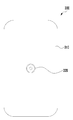
도 3은 본 발명의 다양한 실시예에 따른 전자 장치의 전면을 간략히 도시한 것이다.
도 4는 본 발명의 다양한 실시예에 따른 전자 장치의 블록도이다.
도 5는 본 발명의 다양한 실시예에 따른 전자 장치를 측면에서 바라본 적층 구조를 도시한 것이다.
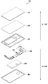
도 6은 본 발명의 다양한 실시예에 따른 전자 장치를 구성하는 각 층을 분리하여 도시한 것이다.
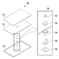
도 7은 본 발명의 다양한 실시예에 따른 전자 장치의 센서의 구조를 도시한 것이다.
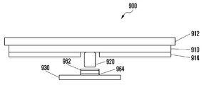
도 8a 및 8b는 본 발명의 다양한 실시예에 따라 전자 장치에 마련되는 카메라의 구조를 도시한 것이다.
도 9a 및 9e는 본 발명의 다양한 실시예에 따른 전기적 구조를 예시한 것이다.
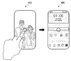
도 10은 본 발명의 다양한 실시예에 따라 사용자의 터치 입력에 의한 화면 변화를 도시한 것이다.
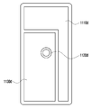
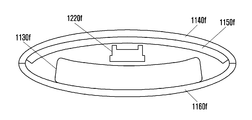
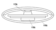
도 11a 내지 11g는 본 발명의 다양한 실시예에 따라 전자 장치의 내부에서 PCB, 센서 및 배터리의 배치 구조를 도시한 것이다.
도 12a 내지 12c는 본 발명의 다양한 실시예에 따른 디스플레이의 배선 형태를 도시한 것이다.
도 13a 및 13b는 본 발명의 다양한 실시예에 따른 디스플레이의 구조를 측면에서 도시한 것이다.
410: 디스플레이
420: 센서
430: 제어 회로
440: 프로세서
450: 메모리
Claims (20)
- 전자 장치에 있어서,
제1방향으로 향하는 제1면, 및 상기 제1방향의 반대인 제2방향으로 향하는 제2면을 포함하는 하우징으로서, 상기 하우징의 제1면의 적어도 일부를 형성하는 투명 기판(transparent substrate)을 포함하는 하우징;
상기 투명 기판 및 상기 하우징의 제2면 사이에 배치되고, 상기 제1방향으로 향하는 제1면, 및 상기 제2방향으로 향하는 제2면을 포함하는 디스플레이;
상기 디스플레이의 제2면의 적어도 일부 및 상기 하우징의 제2면의 적어도 일부 사이에 배치된 적어도 하나의 센서;
상기 적어도 하나의 센서 및 상기 하우징의 제2면의 적어도 일부 사이에 배치된 전기적 구조; 및
상기 전기적 구조와 전기적으로 연결된 제어 회로를 포함하고,
상기 제어 회로는,
상기 전기적 구조를 이용하여, 상기 투명 기판의 적어도 일부에 대한 상기 제2방향의 압력에 의해 상기 전기적 구조 내부에서 발생되거나 변화하는 전기적 신호를 감지하도록 구성된 전자 장치.
- 제 1항에 있어서,
상기 적어도 하나의 센서는,
카메라, 근접 센서, 조도 센서, 지문 인식 센서, 또는 생체 센서 중 적어도 하나를 포함하는 전자 장치.
- 제 1항에 있어서,
상기 전기적 구조는,
상기 적어도 하나의 센서로부터 상기 제2방향으로 이격된 도전성 부재; 및
상기 적어도 하나의 센서의 적어도 일부 및 상기 도전성 부재의 적어도 일부 사이에 배치된 도전성 돔 구조를 포함하고,
상기 제어 회로는, 상기 압력에 의해 상기 도전성 돔 구조의 적어도 일부 및 상기 도전성 부재의 접촉에 의해 발생된 전기적 신호를 감지하도록 구성된 전자 장치.
- 제 1항에 있어서,
상기 전기적 구조는,
상기 적어도 하나의 센서와 적어도 일부 접촉한 제1전극; 및
상기 제1전극과 적어도 일부 접촉한 제2전극을 포함하고,
상기 제어 회로는,
상기 제1전극 또는 상기 제2전극을 이용하여, 상기 제1전극 또는 상기 제2전극의 적어도 일부에서의 전류의 양, 저항, 또는 전압의 변화를 상기 전기적 신호의 변화로서 감지하도록 구성된 전자 장치.
- 제 1항에 있어서,
상기 전기적 구조는,
빛을 방출시키는 발광 구조; 및
상기 발광 구조로부터 방출된 빛을 적어도 일부 수신하는 수광 구조를 포함하고,
상기 제어 회로는,
상기 발광 구조로부터 빛이 방출되어 상기 수광 구조에 도달하는 시간 또는 상기 수광 구조에서 수신된 빛의 양 중 적어도 하나를 상기 전기적 신호의 변화로서 감지하도록 구성된 전자 장치.
- 제 1항에 있어서,
상기 전기적 구조는, 제1전극 및 상기 제1전극으로부터 이격되어 배치된 제2전극을 포함하고,
상기 제어 회로는, 상기 제1전극 및 상기 제2전극 사이에 형성된 정전 용량의 변화를 상기 전기적 신호의 변화로서 감지하도록 구성된 전자 장치.
- 제 1항에 있어서,
상기 전자 장치는,
상기 제어 회로 및 상기 디스플레이와 전기적으로 연결된 프로세서 및 상기 프로세서와 전기적으로 연결된 메모리를 더 포함하고,
상기 메모리는, 실행시에, 상기 프로세서가,
상기 디스플레이에 제1화면을 표시하고,
상기 감지에 응답하여, 상기 제1화면을 복수의 어플리케이션들에 대응하는 복수의 아이콘들이 배치된 제2화면으로 전환하도록 하는 인스트럭션을 저장하는 전자 장치.
- 제 1항에 있어서,
상기 디스플레이는,
상기 투명 기판의 위에서 볼 때, 상기 적어도 하나의 센서와 적어도 일부 중첩하지 않는 제1영역; 및
상기 투명 기판의 위에서 볼 때, 상기 적어도 하나의 센서와 적어도 일부 중첩하는 제2영역을 포함하는 전자 장치.
- 제 8항에 있어서,
상기 디스플레이의 제1영역은, 제1구조를 갖는 제1화소를 포함하고,
상기 디스플레이의 제2영역은, 제2구조를 갖는 제2화소를 포함하는 전자 장치.
- 제 8항에 있어서,
상기 디스플레이의 제2영역의 투과율은,
상기 디스플레이의 제1영역의 투과율보다 높은 전자 장치.
- 제 8항에 있어서,
상기 디스플레이의 제2영역의 단위 면적 당 픽셀 수(pixel per inch; ppi)는,
상기 디스플레이의 제1영역 의 단위 면적 당 픽셀 수보다 낮은 전자 장치.
- 제 8항에 있어서,
상기 디스플레이는,
상기 제1화소 또는 상기 제2화소 중 적어도 하나에 제1신호를 전달하도록 구성된 게이트 배선 및 상기 제1화소 또는 상기 제2화소 중 적어도 하나에 제2신호를 전달하도록 구성된 데이터 배선을 포함하고,
상기 디스플레이의 제1영역을 가로지르는 제1게이트 배선의 형태 또는 제1데이터 배선의 형태 중 적어도 하나는, 상기 디스플레이의 제2영역을 가로지르는 제2게이트 배선의 형태 또는 제2데이터 배선의 형태 중 적어도 하나와 다른 전자 장치.
- 제 8항에 있어서,
상기 전자 장치는, 상기 투명 기판 및 상기 디스플레이 사이에 배치되거나, 상기 디스플레이 내부에 배치된 터치 스크린을 더 포함하고,
상기 터치 스크린은,
상기 투명 기판 및 상기 디스플레이의 제1영역 사이에 배치된 제1터치 전극 패턴; 및
상기 투명 기판 및 상기 디스플레이의 제2영역 사이에 배치된 제2터치 전극 패턴을 포함하는 전자 장치.
- 제 13항에 있어서,
상기 제2터치 전극 패턴은, 상기 제1터치 전극 패턴의 적어도 일부가 제거된 형태인 전자 장치.
- 제 1항에 있어서,
상기 디스플레이는 유기 발광 다이오드를 포함하는 활성(active) 영역, 및 유기 발광 다이오드를 포함하지 않는 비활성(inactive) 영역을 포함하고,
상기 디스플레이의 비활성 영역 중 적어도 일부는 상기 제2방향으로 폴딩된(folded) 전자 장치.
- 제 15항에 있어서,
상기 전자 장치는, 상기 디스플레이와 전기적으로 연결된 디스플레이 구동 집적 회로(Display Driver Integrated Circuit)을 더 포함하고,
상기 디스플레이 구동 집적 회로는, 상기 제2방향으로 폴딩된 적어도 일부에 배치된 전자 장치.
- 제 15항에 있어서,
상기 디스플레이는, 제1폴리머 층, 및 상기 제1폴리머 층의 상기 제2방향으로 향하는 면에 부착된 제2폴리머 층을 포함하고,
상기 제2폴리머 층은, 상기 제2방향으로 폴딩된 적어도 일부에서 적어도 일부 제거된 전자 장치.
- 제 1항에 있어서,
상기 전자 장치는, 상기 디스플레이의 제2면 및 상기 하우징의 제2면 사이에 배치된 압력 센서; 및
상기 압력 센서와 전기적으로 연결된 다른 제어 회로를 더 포함하고,
상기 다른 제어 회로는, 상기 압력 센서를 이용하여, 상기 제2방향의 압력의 정도를 감지하도록 구성된 전자 장치.
- 제 1항에 있어서,
상기 전자 장치는, 지문 센서 또는 안테나 중 적어도 하나를 더 포함하고,
상기 지문 센서 또는 안테나 중 적어도 하나는, 상기 투명 기판 및 상기 디스플레이 사이에 배치되거나, 상기 디스플레이 내부에 배치된 전자 장치.
- 전자 장치에 있어서,
제1방향으로 향하는 제1면, 및 상기 제1방향의 반대인 제2방향으로 향하는 제2면을 포함하는 하우징으로서, 상기 하우징의 제1면의 적어도 일부를 형성하는 투명 기판(transparent substrate)을 포함하는 하우징;
상기 투명 기판 및 상기 하우징의 제2면 사이에 배치되고, 상기 제1방향으로 향하는 제1면, 및 상기 제2방향으로 향하는 제2면을 포함하는 디스플레이;
상기 디스플레이의 제2면의 적어도 일부 및 상기 하우징의 제2면의 적어도 일부 사이에 배치된 카메라 장치;
상기 카메라 장치로부터 상기 제2방향으로 이격되어 배치된 부재;
상기 카메라 장치 및 상기 부재 사이에 배치된 전기적 구조; 및
상기 전기적 구조와 전기적으로 연결된 제어 회로를 포함하고,
상기 제어 회로는,
상기 전기적 구조를 이용하여, 상기 카메라 장치의 상기 제2방향으로의 움직임에 따른 상기 카메라 장치 및 상기 부재 사이의 거리의 변화에 의해 상기 전기적 구조 내부에서 발생되거나 변화하는 전기적 신호를 감지하도록 구성된 전자 장치.
Priority Applications (3)
| Application Number | Priority Date | Filing Date | Title |
|---|---|---|---|
| KR1020160007451A KR102419624B1 (ko) | 2016-01-21 | 2016-01-21 | 전자 장치의 센서 배치 구조 |
| US15/268,474 US10754455B2 (en) | 2016-01-21 | 2016-09-16 | Disposition structure of sensor of electronic device |
| US16/947,924 US11740716B2 (en) | 2016-01-21 | 2020-08-24 | Disposition structure of sensor of electronic device |
Applications Claiming Priority (1)
| Application Number | Priority Date | Filing Date | Title |
|---|---|---|---|
| KR1020160007451A KR102419624B1 (ko) | 2016-01-21 | 2016-01-21 | 전자 장치의 센서 배치 구조 |
Publications (2)
| Publication Number | Publication Date |
|---|---|
| KR20170087635A true KR20170087635A (ko) | 2017-07-31 |
| KR102419624B1 KR102419624B1 (ko) | 2022-07-11 |
Family
ID=59359029
Family Applications (1)
| Application Number | Title | Priority Date | Filing Date |
|---|---|---|---|
| KR1020160007451A Active KR102419624B1 (ko) | 2016-01-21 | 2016-01-21 | 전자 장치의 센서 배치 구조 |
Country Status (2)
| Country | Link |
|---|---|
| US (2) | US10754455B2 (ko) |
| KR (1) | KR102419624B1 (ko) |
Cited By (28)
| Publication number | Priority date | Publication date | Assignee | Title |
|---|---|---|---|---|
| WO2019112314A1 (ko) * | 2017-12-06 | 2019-06-13 | 삼성전자 주식회사 | 디스플레이에서 발생된 노이즈를 차단하기 위한 도전성 부재가 디스플레이와 초음파 센서 사이에 배치된 전자 장치 |
| KR20190080640A (ko) * | 2017-12-28 | 2019-07-08 | 엘지디스플레이 주식회사 | 지문 인식이 가능한 표시 장치 |
| KR20190091711A (ko) * | 2018-01-29 | 2019-08-07 | 삼성전자주식회사 | 플렉서블 디스플레이를 포함하는 전자 장치 |
| KR20190098537A (ko) * | 2018-02-14 | 2019-08-22 | 삼성전자주식회사 | 생체 센서를 포함하는 전자 장치 |
| WO2019172701A1 (en) * | 2018-03-09 | 2019-09-12 | Samsung Electronics Co., Ltd. | Electronic device including antenna |
| WO2020036279A1 (ko) * | 2018-08-17 | 2020-02-20 | 삼성디스플레이 주식회사 | 전자 장치 |
| WO2020067611A1 (ko) * | 2018-09-28 | 2020-04-02 | 삼성디스플레이 주식회사 | 유기 발광 표시 장치 |
| WO2020171585A1 (ko) * | 2019-02-19 | 2020-08-27 | 삼성전자 주식회사 | 센서와 상이한 형상의 개구를 구비하는 디스플레이를 포함하는 전자 장치 |
| KR20200131488A (ko) * | 2019-05-14 | 2020-11-24 | 삼성전자주식회사 | 디스플레이의 광을 이용하여 생체 정보를 획득하기 위한 전자 장치 및 방법 |
| WO2020256496A1 (ko) * | 2019-06-19 | 2020-12-24 | 삼성전자 주식회사 | 불규칙한 패턴이 형성된 디스플레이를 포함하는 전자 장치 |
| KR20210016217A (ko) * | 2019-08-02 | 2021-02-15 | 삼성디스플레이 주식회사 | 전자 패널 및 이를 포함하는 전자 장치 |
| US10923541B2 (en) | 2018-01-30 | 2021-02-16 | Samsung Display Co., Ltd. | Display device |
| US11017733B2 (en) | 2018-03-07 | 2021-05-25 | Samsung Electronics Co., Ltd. | Electronic device for compensating color of display |
| US11087110B2 (en) | 2018-03-05 | 2021-08-10 | Samsung Display Co., Ltd. | Display device including an optical fingerprint sensor |
| KR20210101987A (ko) * | 2020-02-11 | 2021-08-19 | 주식회사 선익시스템 | Oled 디스플레이 소자, 전자 장치 및 oled 디스플레이 소자 제조 방법 |
| KR20210124609A (ko) * | 2020-04-06 | 2021-10-15 | 삼성디스플레이 주식회사 | 생체 센서를 포함하는 표시 장치 및 그것의 동작 방법 |
| US11307685B2 (en) | 2018-04-24 | 2022-04-19 | Samsung Display Co., Ltd. | Display device including a sensor and a protective layer |
| WO2023282660A1 (ko) * | 2021-07-09 | 2023-01-12 | 삼성전자주식회사 | 전자 장치 및 전자 장치의 동작 방법 |
| US20230083578A1 (en) | 2021-09-15 | 2023-03-16 | Lg Display Co., Ltd. | Substrate, display panel and display device comprising the same |
| KR20230066304A (ko) * | 2017-12-27 | 2023-05-15 | 엘지디스플레이 주식회사 | 지문 인식이 가능한 표시 장치 |
| KR20230085123A (ko) * | 2017-12-29 | 2023-06-13 | 엘지디스플레이 주식회사 | 지문 인식이 가능한 표시 장치 |
| US11765928B2 (en) | 2019-12-31 | 2023-09-19 | Samsung Display Co., Ltd. | Display device including transmission area with grooved substrate or lower metal patterns |
| US11824053B2 (en) | 2019-11-18 | 2023-11-21 | Samsung Electronics Co., Ltd. | Electronic device including display and camera device |
| KR20240005627A (ko) * | 2016-09-23 | 2024-01-12 | 삼성디스플레이 주식회사 | 표시 장치 |
| JP2024037788A (ja) * | 2018-10-11 | 2024-03-19 | 京東方科技集團股▲ふん▼有限公司 | アレイ基板、表示パネル及び表示装置 |
| WO2024242450A1 (ko) * | 2023-05-22 | 2024-11-28 | 삼성전자 주식회사 | 레이더 신호를 송수신하는 안테나를 포함하는 전자 장치 |
| US12176357B2 (en) | 2020-12-30 | 2024-12-24 | Lg Display Co., Ltd. | Organic light emitting display device and manufacturing method thereof |
| WO2025216373A1 (ko) * | 2024-04-09 | 2025-10-16 | 삼성전자 주식회사 | 안테나를 포함하는 전자 장치 |
Families Citing this family (33)
| Publication number | Priority date | Publication date | Assignee | Title |
|---|---|---|---|---|
| KR102419624B1 (ko) * | 2016-01-21 | 2022-07-11 | 삼성전자 주식회사 | 전자 장치의 센서 배치 구조 |
| US20190095004A1 (en) * | 2016-06-21 | 2019-03-28 | Crucialtec Co., Ltd. | Fingerprint sensor module and method of manufacturing same |
| CN107562269B (zh) * | 2017-08-28 | 2020-04-17 | 京东方科技集团股份有限公司 | 压力触控结构和显示装置 |
| CN108008765A (zh) * | 2017-11-22 | 2018-05-08 | 广东欧珀移动通信有限公司 | 电子设备 |
| EP3757885B1 (en) * | 2018-02-06 | 2022-06-29 | Shenzhen Goodix Technology Co., Ltd. | Under-screen biometric identification apparatus, biometric identification assembly, and terminal device |
| CN108885696B (zh) * | 2018-02-06 | 2021-03-19 | 深圳市汇顶科技股份有限公司 | 屏下生物特征识别装置和电子设备 |
| KR102415468B1 (ko) | 2018-02-14 | 2022-07-01 | 삼성전자주식회사 | 디스플레이의 아래에 배치된 생체 센서와 디스플레이 사이의 공간을 채우기 위한 충진재를 포함하는 전자 장치 |
| KR102277928B1 (ko) * | 2018-04-25 | 2021-07-16 | 삼성전자주식회사 | 플렉서블 디스플레이 및 이를 구비하는 전자 장치 |
| JP6365962B1 (ja) * | 2018-04-26 | 2018-08-01 | パナソニックIpマネジメント株式会社 | 携帯端末 |
| WO2020024220A1 (zh) * | 2018-08-02 | 2020-02-06 | 深圳市汇顶科技股份有限公司 | 屏下生物特征识别装置和电子设备 |
| CN109446908A (zh) * | 2018-09-27 | 2019-03-08 | 维沃移动通信有限公司 | 一种移动终端 |
| WO2020082369A1 (zh) * | 2018-10-26 | 2020-04-30 | 深圳市汇顶科技股份有限公司 | 屏下生物特征识别装置和电子设备 |
| CN111435185B (zh) * | 2019-01-11 | 2025-12-30 | 北京小米移动软件有限公司 | 偏光片、显示屏、终端及偏光片的制造方法 |
| CN111585375A (zh) * | 2019-02-19 | 2020-08-25 | 三赢科技(深圳)有限公司 | 音圈马达及应用其的摄像头模组和电子装置 |
| KR102774091B1 (ko) * | 2019-04-03 | 2025-02-27 | 삼성전자주식회사 | 디스플레이를 포함하는 전자 장치 |
| CN112055101A (zh) * | 2019-06-05 | 2020-12-08 | 北京小米移动软件有限公司 | 电子设备 |
| CN110491905B (zh) * | 2019-07-16 | 2021-12-03 | 武汉华星光电半导体显示技术有限公司 | 显示面板、显示装置及显示面板的制造方法 |
| US11575865B2 (en) | 2019-07-26 | 2023-02-07 | Samsung Electronics Co., Ltd. | Processing images captured by a camera behind a display |
| CN112670315B (zh) * | 2019-10-15 | 2026-01-13 | 华为技术有限公司 | 一种柔性显示模组和柔性显示装置 |
| KR102928961B1 (ko) | 2020-02-17 | 2026-02-20 | 삼성디스플레이 주식회사 | 표시 장치 및 이를 구비한 전자 기기 |
| CN111308770A (zh) * | 2020-02-26 | 2020-06-19 | 武汉华星光电技术有限公司 | 显示装置 |
| KR20220016342A (ko) * | 2020-07-30 | 2022-02-09 | 삼성디스플레이 주식회사 | 표시 장치 |
| CN112086492B (zh) * | 2020-09-10 | 2022-09-27 | 武汉华星光电半导体显示技术有限公司 | 一种显示面板及显示装置 |
| KR102965006B1 (ko) * | 2021-01-20 | 2026-05-14 | 삼성디스플레이 주식회사 | 표시 장치 |
| US11721001B2 (en) | 2021-02-16 | 2023-08-08 | Samsung Electronics Co., Ltd. | Multiple point spread function based image reconstruction for a camera behind a display |
| US11722796B2 (en) | 2021-02-26 | 2023-08-08 | Samsung Electronics Co., Ltd. | Self-regularizing inverse filter for image deblurring |
| WO2022203364A1 (ko) * | 2021-03-26 | 2022-09-29 | 삼성전자 주식회사 | 피듀셜 마크를 포함하는 하우징을 포함하는 전자 장치 및 그 제조 방법 |
| CN115273653B (zh) | 2021-04-29 | 2024-10-01 | 群创光电股份有限公司 | 显示装置 |
| US12393765B2 (en) | 2021-08-06 | 2025-08-19 | Samsung Electronics Co., Ltd. | Automating search for improved display structure for under-display camera systems |
| US12216277B2 (en) | 2021-10-14 | 2025-02-04 | Samsung Electronics Co., Ltd. | Optical element for deconvolution |
| KR20230081212A (ko) * | 2021-11-30 | 2023-06-07 | 삼성전자주식회사 | 터치 센서 일체형 디스플레이를 포함하는 전자 장치 |
| US12482075B2 (en) | 2022-06-08 | 2025-11-25 | Samsung Electronics Co., Ltd. | Restoring images using deconvolution |
| US12651320B2 (en) | 2022-11-23 | 2026-06-09 | Samsung Electronics Co., Ltd. | Airy-disk correction for deblurring an image |
Citations (6)
| Publication number | Priority date | Publication date | Assignee | Title |
|---|---|---|---|---|
| KR20080075804A (ko) * | 2007-02-13 | 2008-08-19 | 큐알쥐 리미티드 | 경사 터치 제어패널 |
| KR20110056315A (ko) * | 2008-10-08 | 2011-05-26 | 리서치 인 모션 리미티드 | 휴대용 터치 감응성 디스플레이에서 이미지를 팬 및 줌하는 방법 |
| KR20110083394A (ko) * | 2010-01-14 | 2011-07-20 | 엘지전자 주식회사 | 입력 장치 및 이를 구비하는 이동 단말기 |
| US20130135328A1 (en) * | 2011-11-30 | 2013-05-30 | Apple Inc. | Devices and methods for providing access to internal component |
| KR20130083153A (ko) * | 2012-01-12 | 2013-07-22 | 삼성전자주식회사 | 이미지 촬영 및 화상 통화 장치와 방법 |
| KR20150036443A (ko) * | 2012-08-07 | 2015-04-07 | 애플 인크. | 가요성 디스플레이 |
Family Cites Families (14)
| Publication number | Priority date | Publication date | Assignee | Title |
|---|---|---|---|---|
| US20040212555A1 (en) | 2003-04-23 | 2004-10-28 | Falco Mark A. | Portable electronic device with integrated display and camera and method therefore |
| US7808540B2 (en) * | 2007-01-09 | 2010-10-05 | Eastman Kodak Company | Image capture and integrated display apparatus |
| US9131135B2 (en) | 2009-06-09 | 2015-09-08 | Apple Inc. | Electronic device flash shutter |
| US9389721B2 (en) * | 2011-02-09 | 2016-07-12 | Apple Inc. | Snap domes as sensor protection |
| US20120257004A1 (en) * | 2011-04-05 | 2012-10-11 | Polycom, Inc. | Direct Eye-Contact Enhancing Videoconferencing Unit |
| US8965449B2 (en) | 2011-04-07 | 2015-02-24 | Apple Inc. | Devices and methods for providing access to internal component |
| US8947627B2 (en) * | 2011-10-14 | 2015-02-03 | Apple Inc. | Electronic devices having displays with openings |
| US20140129843A1 (en) * | 2012-11-02 | 2014-05-08 | Weidong Shi | Methods and Apparatus for Managing Service Access Using a Touch-Display Device Integrated with Fingerprint Imager |
| US20140133715A1 (en) * | 2012-11-15 | 2014-05-15 | Identity Validation Products, Llc | Display screen with integrated user biometric sensing and verification system |
| KR20150059470A (ko) | 2013-11-22 | 2015-06-01 | 엘지전자 주식회사 | 이동 단말기 |
| US20150296607A1 (en) * | 2014-04-11 | 2015-10-15 | Apple Inc. | Electronic Device With Flexible Printed Circuit Strain Gauge Sensor |
| CN104182727B (zh) * | 2014-05-16 | 2021-07-30 | 深圳印象认知技术有限公司 | 超薄型指纹、掌纹采集装置及指纹、掌纹图像采集方法 |
| US10438046B2 (en) * | 2015-11-02 | 2019-10-08 | Shenzhen GOODIX Technology Co., Ltd. | Multifunction fingerprint sensor having optical sensing against fingerprint spoofing |
| KR102419624B1 (ko) * | 2016-01-21 | 2022-07-11 | 삼성전자 주식회사 | 전자 장치의 센서 배치 구조 |
-
2016
- 2016-01-21 KR KR1020160007451A patent/KR102419624B1/ko active Active
- 2016-09-16 US US15/268,474 patent/US10754455B2/en active Active
-
2020
- 2020-08-24 US US16/947,924 patent/US11740716B2/en active Active
Patent Citations (6)
| Publication number | Priority date | Publication date | Assignee | Title |
|---|---|---|---|---|
| KR20080075804A (ko) * | 2007-02-13 | 2008-08-19 | 큐알쥐 리미티드 | 경사 터치 제어패널 |
| KR20110056315A (ko) * | 2008-10-08 | 2011-05-26 | 리서치 인 모션 리미티드 | 휴대용 터치 감응성 디스플레이에서 이미지를 팬 및 줌하는 방법 |
| KR20110083394A (ko) * | 2010-01-14 | 2011-07-20 | 엘지전자 주식회사 | 입력 장치 및 이를 구비하는 이동 단말기 |
| US20130135328A1 (en) * | 2011-11-30 | 2013-05-30 | Apple Inc. | Devices and methods for providing access to internal component |
| KR20130083153A (ko) * | 2012-01-12 | 2013-07-22 | 삼성전자주식회사 | 이미지 촬영 및 화상 통화 장치와 방법 |
| KR20150036443A (ko) * | 2012-08-07 | 2015-04-07 | 애플 인크. | 가요성 디스플레이 |
Cited By (46)
| Publication number | Priority date | Publication date | Assignee | Title |
|---|---|---|---|---|
| KR20240005627A (ko) * | 2016-09-23 | 2024-01-12 | 삼성디스플레이 주식회사 | 표시 장치 |
| US12266207B2 (en) | 2016-09-23 | 2025-04-01 | Samsung Display Co., Ltd. | Display device |
| US11321959B2 (en) | 2017-12-06 | 2022-05-03 | Samsung Electronics Co., Ltd. | Electronic apparatus in which conductive member for blocking noise generated by display is disposed between display and ultrasonic sensor |
| WO2019112314A1 (ko) * | 2017-12-06 | 2019-06-13 | 삼성전자 주식회사 | 디스플레이에서 발생된 노이즈를 차단하기 위한 도전성 부재가 디스플레이와 초음파 센서 사이에 배치된 전자 장치 |
| KR20230066304A (ko) * | 2017-12-27 | 2023-05-15 | 엘지디스플레이 주식회사 | 지문 인식이 가능한 표시 장치 |
| KR20190080640A (ko) * | 2017-12-28 | 2019-07-08 | 엘지디스플레이 주식회사 | 지문 인식이 가능한 표시 장치 |
| KR20230174205A (ko) * | 2017-12-28 | 2023-12-27 | 엘지디스플레이 주식회사 | 지문 인식이 가능한 표시 장치 |
| KR20230085123A (ko) * | 2017-12-29 | 2023-06-13 | 엘지디스플레이 주식회사 | 지문 인식이 가능한 표시 장치 |
| KR20190091711A (ko) * | 2018-01-29 | 2019-08-07 | 삼성전자주식회사 | 플렉서블 디스플레이를 포함하는 전자 장치 |
| US11329247B2 (en) | 2018-01-29 | 2022-05-10 | Samsung Electronics Co., Ltd. | Electronic device comprising flexible display |
| US10923541B2 (en) | 2018-01-30 | 2021-02-16 | Samsung Display Co., Ltd. | Display device |
| US11469279B2 (en) | 2018-01-30 | 2022-10-11 | Samsung Display Co., Ltd. | Display device |
| US12080094B2 (en) | 2018-02-14 | 2024-09-03 | Samsung Electronics Co., Ltd. | Electronic device including biometric sensor |
| KR20230058369A (ko) * | 2018-02-14 | 2023-05-03 | 삼성전자주식회사 | 생체 센서를 포함하는 전자 장치 |
| KR20190098537A (ko) * | 2018-02-14 | 2019-08-22 | 삼성전자주식회사 | 생체 센서를 포함하는 전자 장치 |
| US11657639B2 (en) | 2018-02-14 | 2023-05-23 | Samsung Electronics Co., Ltd. | Electronic device including biometric sensor |
| US11087110B2 (en) | 2018-03-05 | 2021-08-10 | Samsung Display Co., Ltd. | Display device including an optical fingerprint sensor |
| US12354399B2 (en) | 2018-03-05 | 2025-07-08 | Samsune Bisassigns, Ltd. | Display device |
| US11017733B2 (en) | 2018-03-07 | 2021-05-25 | Samsung Electronics Co., Ltd. | Electronic device for compensating color of display |
| KR20190106555A (ko) * | 2018-03-09 | 2019-09-18 | 삼성전자주식회사 | 안테나를 포함하는 전자 장치 |
| WO2019172701A1 (en) * | 2018-03-09 | 2019-09-12 | Samsung Electronics Co., Ltd. | Electronic device including antenna |
| US11196847B2 (en) | 2018-03-09 | 2021-12-07 | Samsung Electronics Co., Ltd. | Electronic device including antenna |
| US11558496B2 (en) | 2018-03-09 | 2023-01-17 | Samsung Electronics Co., Ltd. | Electronic device including antenna |
| US11307685B2 (en) | 2018-04-24 | 2022-04-19 | Samsung Display Co., Ltd. | Display device including a sensor and a protective layer |
| US11508175B2 (en) | 2018-08-17 | 2022-11-22 | Samsung Display Co., Ltd. | Electronic device |
| WO2020036279A1 (ko) * | 2018-08-17 | 2020-02-20 | 삼성디스플레이 주식회사 | 전자 장치 |
| US12245465B2 (en) | 2018-09-28 | 2025-03-04 | Samsung Display Co., Ltd. | Organic light emitting display device |
| WO2020067611A1 (ko) * | 2018-09-28 | 2020-04-02 | 삼성디스플레이 주식회사 | 유기 발광 표시 장치 |
| KR20200037029A (ko) * | 2018-09-28 | 2020-04-08 | 삼성디스플레이 주식회사 | 유기 발광 표시 장치 |
| JP2024037788A (ja) * | 2018-10-11 | 2024-03-19 | 京東方科技集團股▲ふん▼有限公司 | アレイ基板、表示パネル及び表示装置 |
| WO2020171585A1 (ko) * | 2019-02-19 | 2020-08-27 | 삼성전자 주식회사 | 센서와 상이한 형상의 개구를 구비하는 디스플레이를 포함하는 전자 장치 |
| US11789501B2 (en) | 2019-02-19 | 2023-10-17 | Samsung Electronics Co., Ltd. | Electronic device including display with opening having shape different from that of sensor |
| KR20200131488A (ko) * | 2019-05-14 | 2020-11-24 | 삼성전자주식회사 | 디스플레이의 광을 이용하여 생체 정보를 획득하기 위한 전자 장치 및 방법 |
| WO2020256496A1 (ko) * | 2019-06-19 | 2020-12-24 | 삼성전자 주식회사 | 불규칙한 패턴이 형성된 디스플레이를 포함하는 전자 장치 |
| KR20210016217A (ko) * | 2019-08-02 | 2021-02-15 | 삼성디스플레이 주식회사 | 전자 패널 및 이를 포함하는 전자 장치 |
| US11824053B2 (en) | 2019-11-18 | 2023-11-21 | Samsung Electronics Co., Ltd. | Electronic device including display and camera device |
| US11765928B2 (en) | 2019-12-31 | 2023-09-19 | Samsung Display Co., Ltd. | Display device including transmission area with grooved substrate or lower metal patterns |
| US12302697B2 (en) | 2019-12-31 | 2025-05-13 | Samsung Display Co., Ltd. | Display device including transmission area overlapping component area |
| KR20210101987A (ko) * | 2020-02-11 | 2021-08-19 | 주식회사 선익시스템 | Oled 디스플레이 소자, 전자 장치 및 oled 디스플레이 소자 제조 방법 |
| KR20210124609A (ko) * | 2020-04-06 | 2021-10-15 | 삼성디스플레이 주식회사 | 생체 센서를 포함하는 표시 장치 및 그것의 동작 방법 |
| US12176357B2 (en) | 2020-12-30 | 2024-12-24 | Lg Display Co., Ltd. | Organic light emitting display device and manufacturing method thereof |
| WO2023282660A1 (ko) * | 2021-07-09 | 2023-01-12 | 삼성전자주식회사 | 전자 장치 및 전자 장치의 동작 방법 |
| US20230083578A1 (en) | 2021-09-15 | 2023-03-16 | Lg Display Co., Ltd. | Substrate, display panel and display device comprising the same |
| US12660494B2 (en) | 2021-09-15 | 2026-06-16 | Lg Display Co., Ltd | Substrate, display panel and display device comprising the same |
| WO2024242450A1 (ko) * | 2023-05-22 | 2024-11-28 | 삼성전자 주식회사 | 레이더 신호를 송수신하는 안테나를 포함하는 전자 장치 |
| WO2025216373A1 (ko) * | 2024-04-09 | 2025-10-16 | 삼성전자 주식회사 | 안테나를 포함하는 전자 장치 |
Also Published As
| Publication number | Publication date |
|---|---|
| US11740716B2 (en) | 2023-08-29 |
| US20170212613A1 (en) | 2017-07-27 |
| US20200379588A1 (en) | 2020-12-03 |
| US10754455B2 (en) | 2020-08-25 |
| KR102419624B1 (ko) | 2022-07-11 |
Similar Documents
| Publication | Publication Date | Title |
|---|---|---|
| KR102419624B1 (ko) | 전자 장치의 센서 배치 구조 | |
| KR102446849B1 (ko) | 생체 정보의 위조를 식별하기 위한 전자 장치 및 방법 | |
| KR102735206B1 (ko) | 지문 센서에 입력되는 노이즈를 감소시키는 장치 | |
| CN108153446B (zh) | 包含显示器的电子装置以及制造显示器的方法 | |
| KR102499120B1 (ko) | 안테나를 포함하는 전자 장치 | |
| KR102570000B1 (ko) | 디스플레이를 제어하는 전자 장치 및 이의 동작 방법 | |
| KR101796660B1 (ko) | 지문 인식 기능을 지원하는 전자 장치 및 이의 운용 방법 | |
| KR102401285B1 (ko) | 디스플레이를 포함하는 전자 장치 | |
| CN107688407B (zh) | 具有指纹传感器的电子设备 | |
| KR102737612B1 (ko) | 터치 정확도 향상을 위한 터치 센서의 배치 방법 및 상기 방법을 이용한 전자 장치 | |
| KR102353770B1 (ko) | 디스플레이에 통합된 압력 센서를 포함하는 전자장치 | |
| US11228091B2 (en) | Electronic device including antenna using structure of display panel | |
| KR102752942B1 (ko) | 디스플레이에 통합된 생체 센서를 포함하는 전자장치 | |
| EP3358455A1 (en) | Apparatus and method for controlling fingerprint sensor | |
| EP3226101A1 (en) | Electronic device including display and camera | |
| KR102496410B1 (ko) | 전자 장치 및 전자 장치의 소리 출력 방법 | |
| KR20170113066A (ko) | 디스플레이를 가진 전자 장치 및 그의 이미지 표시 방법 | |
| US20190102016A1 (en) | Display comprising sensing function, and electronic device comprising same | |
| KR20180098466A (ko) | 코너가 둥근 디스플레이를 구비한 전자 장치 | |
| KR102330999B1 (ko) | 전자 장치 및 이의 제어 방법 | |
| KR20190098537A (ko) | 생체 센서를 포함하는 전자 장치 | |
| KR102706129B1 (ko) | 전자 장치 및 전자 장치의 터치 좌표 판단 방법 | |
| KR20170112494A (ko) | 안테나 장치를 포함하는 전자 장치 | |
| KR20170096565A (ko) | 전자 장치 | |
| KR102890456B1 (ko) | 디스플레이에 포함된 픽셀을 이용하여 센서의 위치를 확인하는 방법 및 전자 장치 |
Legal Events
| Date | Code | Title | Description |
|---|---|---|---|
| PA0109 | Patent application |
St.27 status event code: A-0-1-A10-A12-nap-PA0109 |
|
| PG1501 | Laying open of application |
St.27 status event code: A-1-1-Q10-Q12-nap-PG1501 |
|
| P22-X000 | Classification modified |
St.27 status event code: A-2-2-P10-P22-nap-X000 |
|
| A201 | Request for examination | ||
| PA0201 | Request for examination |
St.27 status event code: A-1-2-D10-D11-exm-PA0201 |
|
| D13-X000 | Search requested |
St.27 status event code: A-1-2-D10-D13-srh-X000 |
|
| D14-X000 | Search report completed |
St.27 status event code: A-1-2-D10-D14-srh-X000 |
|
| P22-X000 | Classification modified |
St.27 status event code: A-2-2-P10-P22-nap-X000 |
|
| E902 | Notification of reason for refusal | ||
| PE0902 | Notice of grounds for rejection |
St.27 status event code: A-1-2-D10-D21-exm-PE0902 |
|
| P22-X000 | Classification modified |
St.27 status event code: A-2-2-P10-P22-nap-X000 |
|
| P11-X000 | Amendment of application requested |
St.27 status event code: A-2-2-P10-P11-nap-X000 |
|
| P13-X000 | Application amended |
St.27 status event code: A-2-2-P10-P13-nap-X000 |
|
| E701 | Decision to grant or registration of patent right | ||
| PE0701 | Decision of registration |
St.27 status event code: A-1-2-D10-D22-exm-PE0701 |
|
| GRNT | Written decision to grant | ||
| PR0701 | Registration of establishment |
St.27 status event code: A-2-4-F10-F11-exm-PR0701 |
|
| PR1002 | Payment of registration fee |
St.27 status event code: A-2-2-U10-U11-oth-PR1002 Fee payment year number: 1 |
|
| PG1601 | Publication of registration |
St.27 status event code: A-4-4-Q10-Q13-nap-PG1601 |
|
| P22-X000 | Classification modified |
St.27 status event code: A-4-4-P10-P22-nap-X000 |
|
| P22-X000 | Classification modified |
St.27 status event code: A-4-4-P10-P22-nap-X000 |
|
| PR1001 | Payment of annual fee |
St.27 status event code: A-4-4-U10-U11-oth-PR1001 Fee payment year number: 4 |
|
| U11 | Full renewal or maintenance fee paid |
Free format text: ST27 STATUS EVENT CODE: A-4-4-U10-U11-OTH-PR1001 (AS PROVIDED BY THE NATIONAL OFFICE) Year of fee payment: 4 |
|
| R18 | Changes to party contact information recorded |
Free format text: ST27 STATUS EVENT CODE: A-5-5-R10-R18-OTH-X000 (AS PROVIDED BY THE NATIONAL OFFICE) |
|
| R18-X000 | Changes to party contact information recorded |
St.27 status event code: A-5-5-R10-R18-oth-X000 |
|
| R18 | Changes to party contact information recorded |
Free format text: ST27 STATUS EVENT CODE: A-5-5-R10-R18-OTH-X000 (AS PROVIDED BY THE NATIONAL OFFICE) |
|
| R18-X000 | Changes to party contact information recorded |
St.27 status event code: A-5-5-R10-R18-oth-X000 |
|
| R18 | Changes to party contact information recorded |
Free format text: ST27 STATUS EVENT CODE: A-5-5-R10-R18-OTH-X000 (AS PROVIDED BY THE NATIONAL OFFICE) |
|
| R18-X000 | Changes to party contact information recorded |
St.27 status event code: A-5-5-R10-R18-oth-X000 |