KR20170090184A - 디스차아지 회로를 갖는 퓨즈 메모리 - Google Patents
디스차아지 회로를 갖는 퓨즈 메모리 Download PDFInfo
- Publication number
- KR20170090184A KR20170090184A KR1020160010730A KR20160010730A KR20170090184A KR 20170090184 A KR20170090184 A KR 20170090184A KR 1020160010730 A KR1020160010730 A KR 1020160010730A KR 20160010730 A KR20160010730 A KR 20160010730A KR 20170090184 A KR20170090184 A KR 20170090184A
- Authority
- KR
- South Korea
- Prior art keywords
- fuse
- word line
- program
- read
- circuit
- Prior art date
- Legal status (The legal status is an assumption and is not a legal conclusion. Google has not performed a legal analysis and makes no representation as to the accuracy of the status listed.)
- Granted
Links
Images



Classifications
-
- G—PHYSICS
- G11—INFORMATION STORAGE
- G11C—STATIC STORES
- G11C17/00—Read-only memories programmable only once; Semi-permanent stores, e.g. manually-replaceable information cards
- G11C17/14—Read-only memories programmable only once; Semi-permanent stores, e.g. manually-replaceable information cards in which contents are determined by selectively establishing, breaking or modifying connecting links by permanently altering the state of coupling elements, e.g. PROM
- G11C17/18—Auxiliary circuits, e.g. for writing into memory
-
- G—PHYSICS
- G11—INFORMATION STORAGE
- G11C—STATIC STORES
- G11C17/00—Read-only memories programmable only once; Semi-permanent stores, e.g. manually-replaceable information cards
- G11C17/14—Read-only memories programmable only once; Semi-permanent stores, e.g. manually-replaceable information cards in which contents are determined by selectively establishing, breaking or modifying connecting links by permanently altering the state of coupling elements, e.g. PROM
- G11C17/16—Read-only memories programmable only once; Semi-permanent stores, e.g. manually-replaceable information cards in which contents are determined by selectively establishing, breaking or modifying connecting links by permanently altering the state of coupling elements, e.g. PROM using electrically-fusible links
-
- G—PHYSICS
- G11—INFORMATION STORAGE
- G11C—STATIC STORES
- G11C29/00—Checking stores for correct operation ; Subsequent repair; Testing stores during standby or offline operation
- G11C29/02—Detection or location of defective auxiliary circuits, e.g. defective refresh counters
- G11C29/027—Detection or location of defective auxiliary circuits, e.g. defective refresh counters in fuses
-
- G—PHYSICS
- G11—INFORMATION STORAGE
- G11C—STATIC STORES
- G11C29/00—Checking stores for correct operation ; Subsequent repair; Testing stores during standby or offline operation
- G11C29/70—Masking faults in memories by using spares or by reconfiguring
- G11C29/78—Masking faults in memories by using spares or by reconfiguring using programmable devices
- G11C29/785—Masking faults in memories by using spares or by reconfiguring using programmable devices with redundancy programming schemes
- G11C29/787—Masking faults in memories by using spares or by reconfiguring using programmable devices with redundancy programming schemes using a fuse hierarchy
-
- H—ELECTRICITY
- H10—SEMICONDUCTOR DEVICES; ELECTRIC SOLID-STATE DEVICES NOT OTHERWISE PROVIDED FOR
- H10B—ELECTRONIC MEMORY DEVICES
- H10B20/00—Read-only memory [ROM] devices
- H10B20/20—Programmable ROM [PROM] devices comprising field-effect components
- H10B20/25—One-time programmable ROM [OTPROM] devices, e.g. using electrically-fusible links
-
- H—ELECTRICITY
- H10—SEMICONDUCTOR DEVICES; ELECTRIC SOLID-STATE DEVICES NOT OTHERWISE PROVIDED FOR
- H10D—INORGANIC ELECTRIC SEMICONDUCTOR DEVICES
- H10D1/00—Resistors, capacitors or inductors
-
- H—ELECTRICITY
- H10—SEMICONDUCTOR DEVICES; ELECTRIC SOLID-STATE DEVICES NOT OTHERWISE PROVIDED FOR
- H10W—GENERIC PACKAGES, INTERCONNECTIONS, CONNECTORS OR OTHER CONSTRUCTIONAL DETAILS OF DEVICES COVERED BY CLASS H10
- H10W20/00—Interconnections in chips, wafers or substrates
- H10W20/40—Interconnections external to wafers or substrates, e.g. back-end-of-line [BEOL] metallisations or vias connecting to gate electrodes
- H10W20/49—Adaptable interconnections, e.g. fuses or antifuses
- H10W20/493—Fuses, i.e. interconnections changeable from conductive to non-conductive
Landscapes
- Read Only Memory (AREA)
Abstract
Description
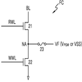
도 2는 도 1의 퓨즈 셀 어레이 내 퓨즈 셀을 설명하는 회로 다이어그램이다.
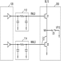
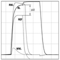
도 3a 및 도 3b는 도 1의 퓨즈 셀 어레이 내 퓨즈 셀의 읽기 마진 감소를 설명하는 도면들이다.
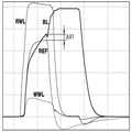
도 4a 및 도 4b는 도 1의 퓨즈 셀 어레이 내 퓨즈 셀의 읽기 마진 증가를 설명하는 도면들이다.
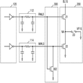
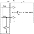
도 5는 본 발명의 실시예에 따른 디스차아지 회로에 연결되는 퓨즈 셀을 설명하는 도면이다.
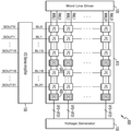
도 6은 본 발명의 실시예에 따른 디스차아지 회로를 갖는 퓨즈 메모리를 설명하는 블락 다이어그램이다.
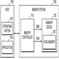
도 7은 본 발명의 실시예들에 따른 디스차아지 회로를 갖는 퓨즈 메모리를 포함하는 메모리 시스템을 설명하는 도면이다.
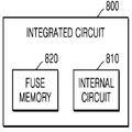
도 8은 본 발명의 실시예들에 따른 디스차아지 회로를 갖는 퓨즈 메모리를 포함하는 집적 회로를 나타내는 블락 다이어그램이다.
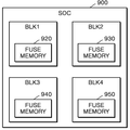
도 9는 본 발명의 실시예들에 따른 디스차아지 회로를 갖는 퓨즈 메모리를 포함하는 시스템 온 칩을 나타내는 블락 다이어그램이다.
도 10은 본 발명의 실시예들에 따른 디스차아지 회로를 갖는 퓨즈 메모리를 포함하는 메모리 시스템을 나타내는 블락 다이어그램이다.
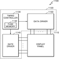
도 11은 본 발명의 실시예들에 따른 디스차아지 회로를 갖는 퓨즈 메모리를 포함하는 디스플레이 시스템을 나타내는 블락 다이어그램이다.
도 12는 본 발명의 실시예들에 따른 디스차아지 회로를 갖는 퓨즈 메모리를 이미지 센서를 나타내는 블락 다이어그램이다.
Claims (10)
- 행들 및 열들로 배열되는 퓨즈 셀들을 구비하는 퓨즈 셀 어레이;
상기 퓨즈 셀 어레이의 상기 행들 마다 적어도 하나 배치되는 디스차아지 회로를 포함하고,
상기 퓨즈 셀들 각각은,
프로그램 전압에 의해 프로그램되고, 상기 프로그램 전압이 인가되는 제1 단이 연결되는 퓨즈 소자;
상기 퓨즈 소자의 제2 단과 비트라인 사이에 연결되고, 독출 워드라인이 그 게이트에 연결되는 독출 트랜지스터; 및
상기 퓨즈 소자의 제2 단과 접지 전압 사이에 연결되고, 프로그램 워드라인이 그 게이트에 연결되는 프로그램 트랜지스터를 포함하고,
상기 디스차아지 회로는 독출되는 상기 퓨즈 셀들의 상기 프로그램 트랜지스터를 턴오프시키는 것을 특징으로 하는 퓨즈 메모리. - 제1항에 있어서,
상기 퓨즈 소자는 상기 제1 단과 상기 제2 단 사이에 연결되는 전기적 퓨즈(e-fuse) 또는 안티퓨즈(Ant-fuse)인 것을 특징으로 하는 퓨즈 메모리. - 제1항에 있어서,
상기 디스차아지 회로는 상기 프로그램 워드라인과 상기 접지 전압 사이에 연결되고, 상기 독출 워드라인이 게이트에 연결되는 엔모스 트랜지스터인 것을 특징으로 하는 퓨즈 메모리. - 제1항에 있어서,
상기 디스차아지 회로는 상기 퓨즈 셀 어레이의 상기 행들의 중앙에 배치되는 것을 특징으로 하는 퓨즈 메모리. - 제1항에 있어서,
상기 디스차아지 회로는 상기 퓨즈 셀 어레이의 상기 행들의 에지에 배치되는 것을 특징으로 하는 퓨즈 메모리. - 독출 워드라인들과 프로그램 워드라인들, 그리고 비트라인들에 연결되는 퓨즈 셀들이 행들 및 열들로 배열되는 퓨즈 셀 어레이;
동작 모드에 따라 상기 행들 중 선택되는 행의 독출 워드라인과 프로그램 워드라인을 선택적으로 구동하는 워드라인 드라이버; 및
상기 비트라인들로 출력되는 상기 퓨즈 셀들의 데이터를 감지 증폭하여 센싱 출력 신호를 출력하는 센스앰프부를 포함하고,
상기 퓨즈 셀 어레이는 상기 행들 마다의 상기 독출 워드라인과 상기 프로그램 워드라인에 연결되는 디스차아지 회로를 포함하고,
상기 디스차아지 회로는 독출 모드에서 선택되는 상기 퓨즈 셀들의 상기 프로그램 워드라인의 전압 레벨을 접지 전압으로 디스차아지시키는 것을 특징으로 하는 퓨즈 메모리. - 제6항에 있어서, 상기 퓨즈 셀들 각각은,
프로그램 전압에 의해 프로그램되고, 상기 프로그램 전압이 인가되는 제1 단이 연결되는 퓨즈 소자;
상기 퓨즈 소자의 제2 단과 비트라인 사이에 연결되고, 상기 독출 워드라인이 그 게이트에 연결되는 독출 트랜지스터; 및
상기 퓨즈 소자의 제2 단과 접지 전압 사이에 연결되고, 상기 프로그램 워드라인이 그 게이트에 연결되는 프로그램 트랜지스터를 포함하는 것을 특징으로 하는 퓨즈 메모리. - 제7항에 있어서,
상기 퓨즈 소자는 상기 제1 단과 상기 제2 단 사이에 연결되는 전기적 퓨즈(e-fuse) 또는 안티퓨즈인 것을 특징으로 하는 퓨즈 메모리. - 제6항에 있어서,
상기 디스차아지 회로는 상기 프로그램 워드라인과 상기 접지 전압 사이에 연결되고, 상기 독출 워드라인이 게이트에 연결되는 엔모스 트랜지스터인 것을 특징으로 하는 퓨즈 메모리. - 제6항에 있어서,
상기 디스차아지 회로는 상기 퓨즈 셀 어레이의 상기 행들의 중앙 또는 에지들 중 상기 워드라인 드라이버에서 가장 먼 거리의 에지에 배치되는 것을 특징으로 하는 퓨즈 메모리.
Priority Applications (2)
| Application Number | Priority Date | Filing Date | Title |
|---|---|---|---|
| KR1020160010730A KR102389817B1 (ko) | 2016-01-28 | 2016-01-28 | 디스차아지 회로를 갖는 퓨즈 메모리 |
| US15/354,304 US9805818B2 (en) | 2016-01-28 | 2016-11-17 | Fuse memory having discharge circuit |
Applications Claiming Priority (1)
| Application Number | Priority Date | Filing Date | Title |
|---|---|---|---|
| KR1020160010730A KR102389817B1 (ko) | 2016-01-28 | 2016-01-28 | 디스차아지 회로를 갖는 퓨즈 메모리 |
Publications (2)
| Publication Number | Publication Date |
|---|---|
| KR20170090184A true KR20170090184A (ko) | 2017-08-07 |
| KR102389817B1 KR102389817B1 (ko) | 2022-04-22 |
Family
ID=59385650
Family Applications (1)
| Application Number | Title | Priority Date | Filing Date |
|---|---|---|---|
| KR1020160010730A Active KR102389817B1 (ko) | 2016-01-28 | 2016-01-28 | 디스차아지 회로를 갖는 퓨즈 메모리 |
Country Status (2)
| Country | Link |
|---|---|
| US (1) | US9805818B2 (ko) |
| KR (1) | KR102389817B1 (ko) |
Families Citing this family (4)
| Publication number | Priority date | Publication date | Assignee | Title |
|---|---|---|---|---|
| US11145379B2 (en) | 2019-10-29 | 2021-10-12 | Key Foundry Co., Ltd. | Electronic fuse cell array structure |
| KR102284263B1 (ko) | 2019-10-29 | 2021-07-30 | 주식회사 키 파운드리 | 이-퓨즈 셀 및 이를 포함하는 비휘발성 메모리 장치 |
| CN111881640B (zh) * | 2020-07-31 | 2024-11-08 | 上海华力微电子有限公司 | 电可编程熔丝系统及其编程方法、读取方法 |
| JP7631047B2 (ja) * | 2021-03-15 | 2025-02-18 | キヤノン株式会社 | 制御装置および素子基板の制御方法 |
Citations (2)
| Publication number | Priority date | Publication date | Assignee | Title |
|---|---|---|---|---|
| US5257230A (en) * | 1989-08-11 | 1993-10-26 | Kabushiki Kaisha Toshiba | Memory device including redundancy cells with programmable fuel elements and process of manufacturing the same |
| KR100845407B1 (ko) * | 2007-02-16 | 2008-07-10 | 매그나칩 반도체 유한회사 | 원-타임-프로그래머블 셀 및 이를 구비하는 otp 메모리 |
Family Cites Families (15)
| Publication number | Priority date | Publication date | Assignee | Title |
|---|---|---|---|---|
| US8767433B2 (en) * | 2004-05-06 | 2014-07-01 | Sidense Corp. | Methods for testing unprogrammed OTP memory |
| US7271988B2 (en) | 2004-08-04 | 2007-09-18 | Taiwan Semiconductor Manufacturing Company | Method and system to protect electrical fuses |
| US7372764B2 (en) | 2004-08-11 | 2008-05-13 | Stmicroelectronics Pvt. Ltd. | Logic device with reduced leakage current |
| KR100610014B1 (ko) | 2004-09-06 | 2006-08-09 | 삼성전자주식회사 | 리키지 전류 보상 가능한 반도체 메모리 장치 |
| US7200064B1 (en) | 2005-10-07 | 2007-04-03 | International Business Machines Corporation | Apparatus and method for providing a reprogrammable electrically programmable fuse |
| US7586787B2 (en) | 2007-09-20 | 2009-09-08 | Kilopass Technology Inc. | Reducing bit line leakage current in non-volatile memories |
| US8400860B2 (en) | 2010-07-20 | 2013-03-19 | Taiwan Semiconductor Manufacturing Company, Ltd. | Electrical fuse memory |
| US8542549B2 (en) | 2011-08-08 | 2013-09-24 | Taiwan Semiconductor Manufacturing Company, Ltd. | Electrical fuse bit cell |
| JP2013051016A (ja) * | 2011-08-31 | 2013-03-14 | Elpida Memory Inc | 半導体装置 |
| US8780604B2 (en) | 2012-06-28 | 2014-07-15 | International Business Machines Corporation | State sensing system for eFuse memory |
| US8643168B1 (en) | 2012-10-16 | 2014-02-04 | Lattice Semiconductor Corporation | Integrated circuit package with input capacitance compensation |
| KR102247562B1 (ko) * | 2014-12-15 | 2021-05-03 | 삼성전자 주식회사 | 멀티 프로그램을 수행하는 오티피 메모리, 및 이를 포함하는 반도체 메모리 장치 |
| KR20160074925A (ko) * | 2014-12-19 | 2016-06-29 | 에스케이하이닉스 주식회사 | 퓨즈 셀 회로, 퓨즈 셀 어레이 및 이를 포함하는 메모리 장치 |
| KR102227124B1 (ko) * | 2014-12-26 | 2021-03-12 | 삼성전자주식회사 | 반도체 장치 |
| KR102248308B1 (ko) * | 2015-04-06 | 2021-05-04 | 에스케이하이닉스 주식회사 | 안티-퓨즈 메모리셀 및 안티-퓨즈 메모리 셀어레이 |
-
2016
- 2016-01-28 KR KR1020160010730A patent/KR102389817B1/ko active Active
- 2016-11-17 US US15/354,304 patent/US9805818B2/en active Active
Patent Citations (2)
| Publication number | Priority date | Publication date | Assignee | Title |
|---|---|---|---|---|
| US5257230A (en) * | 1989-08-11 | 1993-10-26 | Kabushiki Kaisha Toshiba | Memory device including redundancy cells with programmable fuel elements and process of manufacturing the same |
| KR100845407B1 (ko) * | 2007-02-16 | 2008-07-10 | 매그나칩 반도체 유한회사 | 원-타임-프로그래머블 셀 및 이를 구비하는 otp 메모리 |
Also Published As
| Publication number | Publication date |
|---|---|
| US20170221574A1 (en) | 2017-08-03 |
| KR102389817B1 (ko) | 2022-04-22 |
| US9805818B2 (en) | 2017-10-31 |
Similar Documents
| Publication | Publication Date | Title |
|---|---|---|
| US10199118B2 (en) | One-time programmable (OTP) memory device for reading multiple fuse bits | |
| KR101718458B1 (ko) | 퓨즈 어레이를 갖는 반도체 장치 및 그 동작방법 | |
| KR100560243B1 (ko) | Dram 자체 수리를 수행하는 방법, 집적 회로 및 온 칩시스템 | |
| US7184333B2 (en) | Semiconductor memory having a dummy signal line connected to dummy memory cell | |
| US9343175B2 (en) | Fuse data reading circuit having multiple reading modes and related devices, systems and methods | |
| US20010022750A1 (en) | Semiconductor memory device capable of recovering defective bit and a system having the same semiconductor memory device | |
| US20130262740A1 (en) | Semiconductor memory device, systems and methods improving refresh quality for weak cell | |
| US7489576B2 (en) | Semiconductor storage device | |
| KR20160062857A (ko) | 멀티 비트 프로그램을 위한 오티피 메모리 셀 및 오티피 메모리 장치 | |
| US8958258B2 (en) | Semiconductor device and test method thereof | |
| US6351425B1 (en) | Method and circuit for high voltage programming of antifuses, and memory device and computer system using same | |
| CN102110476A (zh) | 具有用于修复缺陷单位单元的冗余电路的半导体存储装置 | |
| US20140063894A1 (en) | E-fuse array circuit and programming method of the same | |
| US9093177B2 (en) | Semiconductor memory device | |
| US9991003B2 (en) | Methods for reading and operating memory device including efuse | |
| KR20190021545A (ko) | 메모리 장치 및 메모리 장치의 동작 방법 | |
| KR102389817B1 (ko) | 디스차아지 회로를 갖는 퓨즈 메모리 | |
| US20240386979A1 (en) | Bit Selection for Power Reduction in Stacking Structure During Memory Programming | |
| US20140241085A1 (en) | Semiconductor memory device for performing disable operation using anti-fuse and method thereof | |
| US8918683B2 (en) | One-time program cell array circuit and memory device including the same | |
| JP2010244615A (ja) | 半導体装置及び半導体装置の書き込み制御方法 | |
| KR100824798B1 (ko) | 에지 서브 어레이에 전체 데이터 패턴을 기입할 수 있는 오픈 비트 라인 구조를 가지는 메모리 코어, 이를 구비한 반도체 메모리 장치, 및 에지 서브 어레이 테스트 방법 | |
| US20080056041A1 (en) | Memory circuit | |
| US9007802B2 (en) | E-fuse array circuit | |
| US20250087293A1 (en) | Memory module, operating method of memory module, and memory system including memory module |
Legal Events
| Date | Code | Title | Description |
|---|---|---|---|
| PA0109 | Patent application |
Patent event code: PA01091R01D Comment text: Patent Application Patent event date: 20160128 |
|
| PG1501 | Laying open of application | ||
| A201 | Request for examination | ||
| PA0201 | Request for examination |
Patent event code: PA02012R01D Patent event date: 20201209 Comment text: Request for Examination of Application Patent event code: PA02011R01I Patent event date: 20160128 Comment text: Patent Application |
|
| E902 | Notification of reason for refusal | ||
| PE0902 | Notice of grounds for rejection |
Comment text: Notification of reason for refusal Patent event date: 20220107 Patent event code: PE09021S01D |
|
| E701 | Decision to grant or registration of patent right | ||
| PE0701 | Decision of registration |
Patent event code: PE07011S01D Comment text: Decision to Grant Registration Patent event date: 20220310 |
|
| GRNT | Written decision to grant | ||
| PR0701 | Registration of establishment |
Comment text: Registration of Establishment Patent event date: 20220419 Patent event code: PR07011E01D |
|
| PR1002 | Payment of registration fee |
Payment date: 20220420 End annual number: 3 Start annual number: 1 |
|
| PG1601 | Publication of registration | ||
| PR1001 | Payment of annual fee |
Payment date: 20250325 Start annual number: 4 End annual number: 4 |