KR20170091627A - 무선 주파수 애플리케이션들을 위한 구조체 - Google Patents
무선 주파수 애플리케이션들을 위한 구조체 Download PDFInfo
- Publication number
- KR20170091627A KR20170091627A KR1020177015538A KR20177015538A KR20170091627A KR 20170091627 A KR20170091627 A KR 20170091627A KR 1020177015538 A KR1020177015538 A KR 1020177015538A KR 20177015538 A KR20177015538 A KR 20177015538A KR 20170091627 A KR20170091627 A KR 20170091627A
- Authority
- KR
- South Korea
- Prior art keywords
- radio frequency
- frequency applications
- layer
- trapping layer
- active layer
- Prior art date
- Legal status (The legal status is an assumption and is not a legal conclusion. Google has not performed a legal analysis and makes no representation as to the accuracy of the status listed.)
- Granted
Links
Images


Classifications
-
- H01L21/02378—
-
- H—ELECTRICITY
- H04—ELECTRIC COMMUNICATION TECHNIQUE
- H04B—TRANSMISSION
- H04B1/00—Details of transmission systems, not covered by a single one of groups H04B3/00 - H04B13/00; Details of transmission systems not characterised by the medium used for transmission
- H04B1/02—Transmitters
- H04B1/03—Constructional details, e.g. casings, housings
-
- H01L21/02381—
-
- H01L21/02529—
-
- H01L21/02532—
-
- H01L21/0262—
-
- H01L21/76254—
-
- H—ELECTRICITY
- H01—ELECTRIC ELEMENTS
- H01M—PROCESSES OR MEANS, e.g. BATTERIES, FOR THE DIRECT CONVERSION OF CHEMICAL ENERGY INTO ELECTRICAL ENERGY
- H01M4/00—Electrodes
- H01M4/02—Electrodes composed of, or comprising, active material
- H01M4/64—Carriers or collectors
- H01M4/66—Selection of materials
- H01M4/663—Selection of materials containing carbon or carbonaceous materials as conductive part, e.g. graphite, carbon fibres
-
- H—ELECTRICITY
- H10—SEMICONDUCTOR DEVICES; ELECTRIC SOLID-STATE DEVICES NOT OTHERWISE PROVIDED FOR
- H10P—GENERIC PROCESSES OR APPARATUS FOR THE MANUFACTURE OR TREATMENT OF DEVICES COVERED BY CLASS H10
- H10P14/00—Formation of materials, e.g. in the shape of layers or pillars
- H10P14/20—Formation of materials, e.g. in the shape of layers or pillars of semiconductor materials
- H10P14/24—Formation of materials, e.g. in the shape of layers or pillars of semiconductor materials using chemical vapour deposition [CVD]
-
- H—ELECTRICITY
- H10—SEMICONDUCTOR DEVICES; ELECTRIC SOLID-STATE DEVICES NOT OTHERWISE PROVIDED FOR
- H10P—GENERIC PROCESSES OR APPARATUS FOR THE MANUFACTURE OR TREATMENT OF DEVICES COVERED BY CLASS H10
- H10P14/00—Formation of materials, e.g. in the shape of layers or pillars
- H10P14/20—Formation of materials, e.g. in the shape of layers or pillars of semiconductor materials
- H10P14/29—Formation of materials, e.g. in the shape of layers or pillars of semiconductor materials characterised by the substrates
- H10P14/2901—Materials
- H10P14/2902—Materials being Group IVA materials
- H10P14/2904—Silicon carbide
-
- H—ELECTRICITY
- H10—SEMICONDUCTOR DEVICES; ELECTRIC SOLID-STATE DEVICES NOT OTHERWISE PROVIDED FOR
- H10P—GENERIC PROCESSES OR APPARATUS FOR THE MANUFACTURE OR TREATMENT OF DEVICES COVERED BY CLASS H10
- H10P14/00—Formation of materials, e.g. in the shape of layers or pillars
- H10P14/20—Formation of materials, e.g. in the shape of layers or pillars of semiconductor materials
- H10P14/29—Formation of materials, e.g. in the shape of layers or pillars of semiconductor materials characterised by the substrates
- H10P14/2901—Materials
- H10P14/2902—Materials being Group IVA materials
- H10P14/2905—Silicon, silicon germanium or germanium
-
- H—ELECTRICITY
- H10—SEMICONDUCTOR DEVICES; ELECTRIC SOLID-STATE DEVICES NOT OTHERWISE PROVIDED FOR
- H10P—GENERIC PROCESSES OR APPARATUS FOR THE MANUFACTURE OR TREATMENT OF DEVICES COVERED BY CLASS H10
- H10P14/00—Formation of materials, e.g. in the shape of layers or pillars
- H10P14/20—Formation of materials, e.g. in the shape of layers or pillars of semiconductor materials
- H10P14/34—Deposited materials, e.g. layers
- H10P14/3402—Deposited materials, e.g. layers characterised by the chemical composition
- H10P14/3404—Deposited materials, e.g. layers characterised by the chemical composition being Group IVA materials
- H10P14/3408—Silicon carbide
-
- H—ELECTRICITY
- H10—SEMICONDUCTOR DEVICES; ELECTRIC SOLID-STATE DEVICES NOT OTHERWISE PROVIDED FOR
- H10P—GENERIC PROCESSES OR APPARATUS FOR THE MANUFACTURE OR TREATMENT OF DEVICES COVERED BY CLASS H10
- H10P14/00—Formation of materials, e.g. in the shape of layers or pillars
- H10P14/20—Formation of materials, e.g. in the shape of layers or pillars of semiconductor materials
- H10P14/34—Deposited materials, e.g. layers
- H10P14/3402—Deposited materials, e.g. layers characterised by the chemical composition
- H10P14/3404—Deposited materials, e.g. layers characterised by the chemical composition being Group IVA materials
- H10P14/3411—Silicon, silicon germanium or germanium
-
- H—ELECTRICITY
- H10—SEMICONDUCTOR DEVICES; ELECTRIC SOLID-STATE DEVICES NOT OTHERWISE PROVIDED FOR
- H10P—GENERIC PROCESSES OR APPARATUS FOR THE MANUFACTURE OR TREATMENT OF DEVICES COVERED BY CLASS H10
- H10P36/00—Gettering within semiconductor bodies
- H10P36/03—Gettering within semiconductor bodies within silicon bodies
- H10P36/07—Gettering within semiconductor bodies within silicon bodies of silicon-on-insulator structures
-
- H—ELECTRICITY
- H10—SEMICONDUCTOR DEVICES; ELECTRIC SOLID-STATE DEVICES NOT OTHERWISE PROVIDED FOR
- H10P—GENERIC PROCESSES OR APPARATUS FOR THE MANUFACTURE OR TREATMENT OF DEVICES COVERED BY CLASS H10
- H10P90/00—Preparation of wafers not covered by a single main group of this subclass, e.g. wafer reinforcement
- H10P90/19—Preparing inhomogeneous wafers
- H10P90/1904—Preparing vertically inhomogeneous wafers
- H10P90/1906—Preparing SOI wafers
- H10P90/1914—Preparing SOI wafers using bonding
- H10P90/1916—Preparing SOI wafers using bonding with separation or delamination along an ion implanted layer, e.g. Smart-cut
-
- H—ELECTRICITY
- H10—SEMICONDUCTOR DEVICES; ELECTRIC SOLID-STATE DEVICES NOT OTHERWISE PROVIDED FOR
- H10P—GENERIC PROCESSES OR APPARATUS FOR THE MANUFACTURE OR TREATMENT OF DEVICES COVERED BY CLASS H10
- H10P90/00—Preparation of wafers not covered by a single main group of this subclass, e.g. wafer reinforcement
- H10P90/19—Preparing inhomogeneous wafers
- H10P90/1904—Preparing vertically inhomogeneous wafers
- H10P90/1906—Preparing SOI wafers
- H10P90/1914—Preparing SOI wafers using bonding
- H10P90/1918—Preparing SOI wafers using bonding including charge trapping layers, e.g. polycrystalline materials
-
- H—ELECTRICITY
- H10—SEMICONDUCTOR DEVICES; ELECTRIC SOLID-STATE DEVICES NOT OTHERWISE PROVIDED FOR
- H10W—GENERIC PACKAGES, INTERCONNECTIONS, CONNECTORS OR OTHER CONSTRUCTIONAL DETAILS OF DEVICES COVERED BY CLASS H10
- H10W10/00—Isolation regions in semiconductor bodies between components of integrated devices
- H10W10/10—Isolation regions comprising dielectric materials
- H10W10/181—Semiconductor-on-insulator [SOI] isolation regions, e.g. buried oxide regions of SOI wafers
-
- H—ELECTRICITY
- H10—SEMICONDUCTOR DEVICES; ELECTRIC SOLID-STATE DEVICES NOT OTHERWISE PROVIDED FOR
- H10D—INORGANIC ELECTRIC SEMICONDUCTOR DEVICES
- H10D64/00—Electrodes of devices having potential barriers
- H10D64/01—Manufacture or treatment
- H10D64/031—Manufacture or treatment of data-storage electrodes
- H10D64/037—Manufacture or treatment of data-storage electrodes comprising charge-trapping insulators
-
- H—ELECTRICITY
- H10—SEMICONDUCTOR DEVICES; ELECTRIC SOLID-STATE DEVICES NOT OTHERWISE PROVIDED FOR
- H10N—ELECTRIC SOLID-STATE DEVICES NOT OTHERWISE PROVIDED FOR
- H10N30/00—Piezoelectric or electrostrictive devices
- H10N30/80—Constructional details
- H10N30/87—Electrodes or interconnections, e.g. leads or terminals
- H10N30/877—Conductive materials
-
- H—ELECTRICITY
- H10—SEMICONDUCTOR DEVICES; ELECTRIC SOLID-STATE DEVICES NOT OTHERWISE PROVIDED FOR
- H10P—GENERIC PROCESSES OR APPARATUS FOR THE MANUFACTURE OR TREATMENT OF DEVICES COVERED BY CLASS H10
- H10P14/00—Formation of materials, e.g. in the shape of layers or pillars
- H10P14/60—Formation of materials, e.g. in the shape of layers or pillars of insulating materials
- H10P14/69—Inorganic materials
- H10P14/6903—Inorganic materials containing silicon
- H10P14/6905—Inorganic materials containing silicon being a silicon carbide or silicon carbonitride and not containing oxygen, e.g. SiC or SiC:H
-
- H—ELECTRICITY
- H10—SEMICONDUCTOR DEVICES; ELECTRIC SOLID-STATE DEVICES NOT OTHERWISE PROVIDED FOR
- H10W—GENERIC PACKAGES, INTERCONNECTIONS, CONNECTORS OR OTHER CONSTRUCTIONAL DETAILS OF DEVICES COVERED BY CLASS H10
- H10W10/00—Isolation regions in semiconductor bodies between components of integrated devices
- H10W10/01—Manufacture or treatment
- H10W10/011—Manufacture or treatment of isolation regions comprising dielectric materials
- H10W10/019—Manufacture or treatment of isolation regions comprising dielectric materials using epitaxial passivated integrated circuit [EPIC] processes
-
- H—ELECTRICITY
- H10—SEMICONDUCTOR DEVICES; ELECTRIC SOLID-STATE DEVICES NOT OTHERWISE PROVIDED FOR
- H10W—GENERIC PACKAGES, INTERCONNECTIONS, CONNECTORS OR OTHER CONSTRUCTIONAL DETAILS OF DEVICES COVERED BY CLASS H10
- H10W10/00—Isolation regions in semiconductor bodies between components of integrated devices
- H10W10/10—Isolation regions comprising dielectric materials
-
- Y—GENERAL TAGGING OF NEW TECHNOLOGICAL DEVELOPMENTS; GENERAL TAGGING OF CROSS-SECTIONAL TECHNOLOGIES SPANNING OVER SEVERAL SECTIONS OF THE IPC; TECHNICAL SUBJECTS COVERED BY FORMER USPC CROSS-REFERENCE ART COLLECTIONS [XRACs] AND DIGESTS
- Y02—TECHNOLOGIES OR APPLICATIONS FOR MITIGATION OR ADAPTATION AGAINST CLIMATE CHANGE
- Y02E—REDUCTION OF GREENHOUSE GAS [GHG] EMISSIONS, RELATED TO ENERGY GENERATION, TRANSMISSION OR DISTRIBUTION
- Y02E60/00—Enabling technologies; Technologies with a potential or indirect contribution to GHG emissions mitigation
- Y02E60/10—Energy storage using batteries
Landscapes
- Chemical & Material Sciences (AREA)
- Engineering & Computer Science (AREA)
- Materials Engineering (AREA)
- Chemical Kinetics & Catalysis (AREA)
- Electrochemistry (AREA)
- General Chemical & Material Sciences (AREA)
- Computer Networks & Wireless Communication (AREA)
- Signal Processing (AREA)
- Semiconductor Integrated Circuits (AREA)
- Crystals, And After-Treatments Of Crystals (AREA)
- Recrystallisation Techniques (AREA)
- Micromachines (AREA)
Abstract
Description
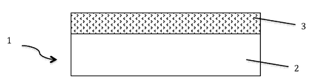
도 1은 기판 및 트래핑 층을 포함하는, 본 발명에 따른 무선 주파수 애플리케이션들을 위한 구조체를 표현한다.
도 2는 최신 기술에 따른 구조체들 및 본 발명에 따른 구조체의 저항률의 비교 곡선들을 도시한다.
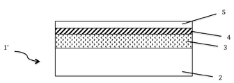
도 3a 및 도 3b는 활성층을 더 포함하는 본 발명에 따른 무선 주파수 애플리케이션들을 위한 구조체를 각각 표현한다.
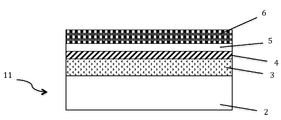
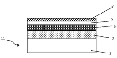
도 4a 및 도 4b는 마이크로전자 디바이스를 더 포함하는 본 발명에 따른 무선 주파수 애플리케이션들을 위한 구조체를 각각 표현한다.

Claims (19)
- 무선 주파수 애플리케이션들을 위한 구조체(1, 1', 11)로서,
반도체 지지 기판(2);
상기 지지 기판(2) 상에 배열되는 트래핑 층(3);을 포함하고,
상기 트래핑 층(3)은 미리 결정된 결함 밀도보다 큰 결함 밀도를 포함하고, 상기 미리 결정된 결함 밀도는, 상기 트래핑 층(3)의 전기 저항률이 온도 범위 [-20 ℃; +120 ℃]에 걸쳐 10 kohm.cm 이상인 결함 밀도인,
무선 주파수 애플리케이션들을 위한 구조체(1, 1', 11). - 제 1 항에 있어서,
상기 트래핑 층(3)은 20 ℃에서, 10 kOhm.cm 초과, 바람직하게는 50 kOhm.cm 초과의 저항률을 갖는,
무선 주파수 애플리케이션들을 위한 구조체(1, 1', 11). - 제 1 항 또는 제 2 항에 있어서,
상기 트래핑 층(3)과 상기 지지 기판(2) 사이의 열 팽창 계수에서의 차이는 100 ℃ 내지 1200 ℃에서 5 ppm/K 미만인,
무선 주파수 애플리케이션들을 위한 구조체(1, 1', 11). - 제 1 항 내지 제 3 항 중 어느 한 항에 있어서,
상기 트래핑 층(3)은 20 nm 미만, 바람직하게는 10 nm 미만인 크기의 마이크로구조체들을 포함하는,
무선 주파수 애플리케이션들을 위한 구조체(1, 1', 11). - 제 1 항 내지 제 4 항 중 어느 한 항에 있어서,
상기 트래핑 층(3)은 다공성 또는 다결정 재료를 포함하는,
무선 주파수 애플리케이션들을 위한 구조체(1, 1', 11). - 제 1 항 내지 제 5 항 중 어느 한 항에 있어서,
상기 트래핑 층(3)은 1 내지 20%의 탄소를 포함하는 다결정 실리콘을 포함하는,
무선 주파수 애플리케이션들을 위한 구조체(1, 1', 11). - 제 1 항 내지 제 6 항 중 어느 한 항에 있어서,
상기 트래핑 층(3)의 두께는 10 내지 50 μm, 바람직하게는 20 내지 30 μm인,
무선 주파수 애플리케이션들을 위한 구조체(1, 1', 11). - 제 1 항 내지 제 7 항 중 어느 한 항에 있어서,
상기 지지 기판(2)은 실리콘, 실리콘 게르마늄 및 실리콘 카바이드로부터 선택되는 재료들 중 적어도 하나를 포함하는,
무선 주파수 애플리케이션들을 위한 구조체(1, 1', 11). - 제 1 항 내지 제 8 항 중 어느 한 항에 있어서,
상기 지지 기판(2)의 저항률은 10 내지 2000 Ohm.cm인,
무선 주파수 애플리케이션들을 위한 구조체(1, 1', 11). - 제 1 항 내지 제 9 항 중 어느 한 항에 있어서,
상기 트래핑 층(3) 상에 활성층(5)이 배열되는,
무선 주파수 애플리케이션들을 위한 구조체(1, 1', 11). - 제 10 항에 있어서,
상기 활성층(5)은 반도체 재료로 형성되는,
무선 주파수 애플리케이션들을 위한 구조체(1, 1', 11). - 제 10 항에 있어서,
상기 활성층(5)은 압전 재료(piezoelectric material)로 형성되는,
무선 주파수 애플리케이션들을 위한 구조체(1, 1', 11). - 제 10 항 내지 제 12 항 중 어느 한 항에 있어서,
상기 활성층(5)의 두께는 10 내지 50 μm인,
무선 주파수 애플리케이션들을 위한 구조체(1, 1', 11). - 제 10 항 내지 제 13 항 중 어느 한 항에 있어서,
상기 트래핑 층(3)과 상기 활성층(5) 사이에 유전체층(4)이 배열되는,
무선 주파수 애플리케이션들을 위한 구조체(1, 1', 11). - 제 14 항에 있어서,
상기 유전체층(4)은 10 nm 내지 6 μm인,
무선 주파수 애플리케이션들을 위한 구조체(1, 1', 11). - 제 10 항 내지 제 15 항 중 어느 한 항에 있어서,
상기 활성층(5)에 또는 상기 활성층(5) 상에 적어도 하나의 마이크로전자 디바이스가 존재하고, 상기 마이크로전자 디바이스는 스위칭 회로 또는 안테나 적응 회로(antenna adaptation circuit) 또는 무선 주파수 전력 증폭 회로(radiofrequency power amplification circuit)인,
무선 주파수 애플리케이션들을 위한 구조체(1, 1', 11). - 제 10 항 내지 제 16 항 중 어느 한 항에 있어서,
상기 활성층(5)에 또는 상기 활성층(5) 상에 적어도 하나의 마이크로전자 디바이스가 존재하고, 상기 마이크로전자 디바이스는 복수의 능동 컴포넌트들(active components) 및 복수의 수동 컴포넌트들(passive components)을 포함하는,
무선 주파수 애플리케이션들을 위한 구조체(1, 1', 11). - 제 10 항 내지 제 16 항 중 어느 한 항에 있어서,
상기 활성층(5)에 또는 상기 활성층(5) 상에 적어도 하나의 마이크로전자 디바이스가 존재하고, 상기 마이크로전자 디바이스는 옴-접촉 마이크로스위치(ohmic-contact microswitch) 또는 용량성 마이크로스위치로 이루어진 하나의 MEMS 스위칭 엘리먼트 및 적어도 하나의 제어 엘리먼트를 포함하는,
무선 주파수 애플리케이션들을 위한 구조체(1, 1', 11). - 제 10 항 내지 제 15 항 중 어느 한 항에 있어서,
상기 활성층(5)에 또는 상기 활성층(5) 상에 적어도 하나의 마이크로전자 디바이스가 존재하고, 상기 마이크로전자 디바이스는 체적 또는 표면 음파 전파( surface sound wave propagation)에 의해 동작하는 무선 주파수 필터인,
무선 주파수 애플리케이션들을 위한 구조체(1, 1', 11).
Applications Claiming Priority (3)
| Application Number | Priority Date | Filing Date | Title |
|---|---|---|---|
| FR1402801A FR3029682B1 (fr) | 2014-12-04 | 2014-12-04 | Substrat semi-conducteur haute resistivite et son procede de fabrication |
| FR1402801 | 2014-12-04 | ||
| PCT/FR2015/052494 WO2016087728A1 (fr) | 2014-12-04 | 2015-09-17 | Structure pour applications radiofréquences |
Publications (2)
| Publication Number | Publication Date |
|---|---|
| KR20170091627A true KR20170091627A (ko) | 2017-08-09 |
| KR102395398B1 KR102395398B1 (ko) | 2022-05-10 |
Family
ID=53039463
Family Applications (1)
| Application Number | Title | Priority Date | Filing Date |
|---|---|---|---|
| KR1020177015538A Active KR102395398B1 (ko) | 2014-12-04 | 2015-09-17 | 무선 주파수 애플리케이션들을 위한 구조체 |
Country Status (8)
| Country | Link |
|---|---|
| US (1) | US10250282B2 (ko) |
| EP (2) | EP3872839A1 (ko) |
| JP (1) | JP6612872B2 (ko) |
| KR (1) | KR102395398B1 (ko) |
| CN (1) | CN107004572B (ko) |
| FR (1) | FR3029682B1 (ko) |
| SG (1) | SG11201704516QA (ko) |
| WO (1) | WO2016087728A1 (ko) |
Cited By (2)
| Publication number | Priority date | Publication date | Assignee | Title |
|---|---|---|---|---|
| KR20210020024A (ko) * | 2018-06-14 | 2021-02-23 | 신에쯔 한도타이 가부시키가이샤 | 첩합soi웨이퍼의 제조방법 및 첩합soi웨이퍼 |
| KR20210027261A (ko) * | 2018-07-05 | 2021-03-10 | 소이텍 | 집적 무선 주파수 디바이스를 위한 기판 및 이를 제조하기 위한 방법 |
Families Citing this family (26)
| Publication number | Priority date | Publication date | Assignee | Title |
|---|---|---|---|---|
| FR3037438B1 (fr) | 2015-06-09 | 2017-06-16 | Soitec Silicon On Insulator | Procede de fabrication d'un element semi-conducteur comprenant une couche de piegeage de charges |
| US10523178B2 (en) | 2015-08-25 | 2019-12-31 | Avago Technologies International Sales Pte. Limited | Surface acoustic wave (SAW) resonator |
| US10530327B2 (en) * | 2015-08-25 | 2020-01-07 | Avago Technologies International Sales Pte. Limited | Surface acoustic wave (SAW) resonator |
| US10541667B2 (en) * | 2015-08-25 | 2020-01-21 | Avago Technologies International Sales Pte. Limited | Surface acoustic wave (SAW) resonator having trap-rich region |
| US10181428B2 (en) * | 2015-08-28 | 2019-01-15 | Skyworks Solutions, Inc. | Silicon on porous silicon |
| EP3144958B1 (en) | 2015-09-17 | 2021-03-17 | Soitec | Structure for radiofrequency applications and process for manufacturing such a structure |
| JP6947158B2 (ja) * | 2016-02-25 | 2021-10-13 | 日本ゼオン株式会社 | 熱伝導シートおよびその製造方法、ならびに放熱装置 |
| FR3053532B1 (fr) * | 2016-06-30 | 2018-11-16 | Soitec | Structure hybride pour dispositif a ondes acoustiques de surface |
| FR3058561B1 (fr) | 2016-11-04 | 2018-11-02 | Soitec | Procede de fabrication d'un element semi-conducteur comprenant un substrat hautement resistif |
| FR3062238A1 (fr) | 2017-01-26 | 2018-07-27 | Soitec | Support pour une structure semi-conductrice |
| FR3062517B1 (fr) | 2017-02-02 | 2019-03-15 | Soitec | Structure pour application radiofrequence |
| US10784348B2 (en) | 2017-03-23 | 2020-09-22 | Qualcomm Incorporated | Porous semiconductor handle substrate |
| US11063117B2 (en) * | 2017-04-20 | 2021-07-13 | Taiwan Semiconductor Manufacturing Co., Ltd. | Semiconductor device structure having carrier-trapping layers with different grain sizes |
| FR3067517B1 (fr) | 2017-06-13 | 2019-07-12 | Commissariat A L'energie Atomique Et Aux Energies Alternatives | Substrat soi compatible avec les technologies rfsoi et fdsoi |
| FR3079662B1 (fr) * | 2018-03-30 | 2020-02-28 | Soitec | Substrat pour applications radiofrequences et procede de fabrication associe |
| FR3098642B1 (fr) * | 2019-07-12 | 2021-06-11 | Soitec Silicon On Insulator | procédé de fabrication d'une structure comprenant une couche mince reportée sur un support muni d’une couche de piégeage de charges |
| WO2021015816A1 (en) * | 2019-07-19 | 2021-01-28 | Iqe Plc | Semiconductor material having tunable permittivity and tunable thermal conductivity |
| CN113629182A (zh) * | 2020-05-08 | 2021-11-09 | 济南晶正电子科技有限公司 | 一种tc-saw复合衬底及其制备方法 |
| CN111884616B (zh) * | 2020-07-23 | 2021-04-13 | 中国科学院上海微系统与信息技术研究所 | 一种衬底基板/压电材料薄膜结构及其制备方法和应用 |
| US20220116014A1 (en) * | 2020-10-13 | 2022-04-14 | RF360 Europe GmbH | Surface acoustic wave (saw) device with high permittivity dielectric for intermodulation distortion improvement |
| CN112260660B (zh) * | 2020-10-21 | 2023-03-03 | 济南晶正电子科技有限公司 | 一种复合基底、复合薄膜及其制备方法 |
| FR3117668B1 (fr) * | 2020-12-16 | 2022-12-23 | Commissariat Energie Atomique | Structure amelioree de substrat rf et procede de realisation |
| CN112750686B (zh) * | 2020-12-30 | 2021-12-07 | 济南晶正电子科技有限公司 | 一种多层衬底、电子元器件及多层衬底制备方法 |
| JP2023054965A (ja) * | 2021-10-05 | 2023-04-17 | 信越半導体株式会社 | シリコンウエーハ及びsoiウエーハ並びにそれらの製造方法 |
| FR3136325B1 (fr) * | 2022-06-02 | 2025-10-03 | Soitec Silicon On Insulator | Dispositif a ondes elastiques de surface |
| EP4533661A1 (fr) * | 2022-06-02 | 2025-04-09 | Soitec | Procédé de fabrication d'un dispositif à ondes élastiques de surface |
Citations (4)
| Publication number | Priority date | Publication date | Assignee | Title |
|---|---|---|---|---|
| US5637883A (en) * | 1995-02-27 | 1997-06-10 | The United States Of America As Represented By The Secretary Of The Navy | Optically addressed spatial light modulator using an intrinsic semiconductor active material and high resistivity cladding layers |
| KR20060118437A (ko) * | 2003-09-26 | 2006-11-23 | 위니베르시트카솔리끄드루뱅 | 저항손을 감소시키는 다층 반도체 구조의 제조 방법 |
| KR20130137013A (ko) * | 2010-12-24 | 2013-12-13 | 아이오 세미컨덕터, 인코포레이티드 | 반도체 소자들을 위한 트랩 리치 층 |
| KR20140027153A (ko) * | 2011-03-22 | 2014-03-06 | 소이텍 | 무선 주파수 응용들을 위한 절연체 위 반도체형 기판의 제조 방법 |
Family Cites Families (4)
| Publication number | Priority date | Publication date | Assignee | Title |
|---|---|---|---|---|
| JP4983010B2 (ja) * | 2005-11-30 | 2012-07-25 | 富士通株式会社 | 圧電素子及びその製造方法 |
| JP2009231376A (ja) * | 2008-03-19 | 2009-10-08 | Shin Etsu Handotai Co Ltd | Soiウェーハ及び半導体デバイスならびにsoiウェーハの製造方法 |
| US8536021B2 (en) * | 2010-12-24 | 2013-09-17 | Io Semiconductor, Inc. | Trap rich layer formation techniques for semiconductor devices |
| KR101876579B1 (ko) * | 2012-09-13 | 2018-07-10 | 매그나칩 반도체 유한회사 | 전력용 반도체 소자 및 그 소자의 제조 방법 |
-
2014
- 2014-12-04 FR FR1402801A patent/FR3029682B1/fr active Active
-
2015
- 2015-09-17 KR KR1020177015538A patent/KR102395398B1/ko active Active
- 2015-09-17 EP EP21170134.7A patent/EP3872839A1/fr active Pending
- 2015-09-17 CN CN201580065277.5A patent/CN107004572B/zh active Active
- 2015-09-17 WO PCT/FR2015/052494 patent/WO2016087728A1/fr not_active Ceased
- 2015-09-17 JP JP2017529767A patent/JP6612872B2/ja active Active
- 2015-09-17 US US15/531,976 patent/US10250282B2/en active Active
- 2015-09-17 SG SG11201704516QA patent/SG11201704516QA/en unknown
- 2015-09-17 EP EP15788467.7A patent/EP3227905B1/fr active Active
Patent Citations (4)
| Publication number | Priority date | Publication date | Assignee | Title |
|---|---|---|---|---|
| US5637883A (en) * | 1995-02-27 | 1997-06-10 | The United States Of America As Represented By The Secretary Of The Navy | Optically addressed spatial light modulator using an intrinsic semiconductor active material and high resistivity cladding layers |
| KR20060118437A (ko) * | 2003-09-26 | 2006-11-23 | 위니베르시트카솔리끄드루뱅 | 저항손을 감소시키는 다층 반도체 구조의 제조 방법 |
| KR20130137013A (ko) * | 2010-12-24 | 2013-12-13 | 아이오 세미컨덕터, 인코포레이티드 | 반도체 소자들을 위한 트랩 리치 층 |
| KR20140027153A (ko) * | 2011-03-22 | 2014-03-06 | 소이텍 | 무선 주파수 응용들을 위한 절연체 위 반도체형 기판의 제조 방법 |
Cited By (2)
| Publication number | Priority date | Publication date | Assignee | Title |
|---|---|---|---|---|
| KR20210020024A (ko) * | 2018-06-14 | 2021-02-23 | 신에쯔 한도타이 가부시키가이샤 | 첩합soi웨이퍼의 제조방법 및 첩합soi웨이퍼 |
| KR20210027261A (ko) * | 2018-07-05 | 2021-03-10 | 소이텍 | 집적 무선 주파수 디바이스를 위한 기판 및 이를 제조하기 위한 방법 |
Also Published As
| Publication number | Publication date |
|---|---|
| EP3227905B1 (fr) | 2021-08-18 |
| EP3872839A1 (fr) | 2021-09-01 |
| FR3029682A1 (fr) | 2016-06-10 |
| FR3029682B1 (fr) | 2017-12-29 |
| US10250282B2 (en) | 2019-04-02 |
| EP3227905A1 (fr) | 2017-10-11 |
| SG11201704516QA (en) | 2017-07-28 |
| JP2018501651A (ja) | 2018-01-18 |
| CN107004572B (zh) | 2020-05-22 |
| WO2016087728A1 (fr) | 2016-06-09 |
| US20170331501A1 (en) | 2017-11-16 |
| JP6612872B2 (ja) | 2019-11-27 |
| KR102395398B1 (ko) | 2022-05-10 |
| CN107004572A (zh) | 2017-08-01 |
Similar Documents
| Publication | Publication Date | Title |
|---|---|---|
| KR102395398B1 (ko) | 무선 주파수 애플리케이션들을 위한 구조체 | |
| JP2018501651A5 (ko) | ||
| CN106575637B (zh) | 用于射频应用的结构 | |
| JP7053502B2 (ja) | 無線周波数用途のための構造 | |
| US20200336127A1 (en) | Hybrid structure for a surface acoustic wave device | |
| US12418120B2 (en) | Structure for radio frequency applications | |
| TWI849089B (zh) | 供無線射頻應用之包含埋置多孔層之半導體結構 | |
| US20210183691A1 (en) | Substrate for an integrated radiofrequency device, and process for manufacturing same | |
| JP2021520755A (ja) | フィルムバルク音響波共振器およびその製造方法 | |
| TW202006896A (zh) | 集成射頻元件用底材及其製作方法 |
Legal Events
| Date | Code | Title | Description |
|---|---|---|---|
| PA0105 | International application |
St.27 status event code: A-0-1-A10-A15-nap-PA0105 |
|
| PG1501 | Laying open of application |
St.27 status event code: A-1-1-Q10-Q12-nap-PG1501 |
|
| A201 | Request for examination | ||
| PA0201 | Request for examination |
St.27 status event code: A-1-2-D10-D11-exm-PA0201 |
|
| E902 | Notification of reason for refusal | ||
| PE0902 | Notice of grounds for rejection |
St.27 status event code: A-1-2-D10-D21-exm-PE0902 |
|
| E13-X000 | Pre-grant limitation requested |
St.27 status event code: A-2-3-E10-E13-lim-X000 |
|
| P11-X000 | Amendment of application requested |
St.27 status event code: A-2-2-P10-P11-nap-X000 |
|
| P13-X000 | Application amended |
St.27 status event code: A-2-2-P10-P13-nap-X000 |
|
| E701 | Decision to grant or registration of patent right | ||
| PE0701 | Decision of registration |
St.27 status event code: A-1-2-D10-D22-exm-PE0701 |
|
| GRNT | Written decision to grant | ||
| PR0701 | Registration of establishment |
St.27 status event code: A-2-4-F10-F11-exm-PR0701 |
|
| PR1002 | Payment of registration fee |
St.27 status event code: A-2-2-U10-U12-oth-PR1002 Fee payment year number: 1 |
|
| PG1601 | Publication of registration |
St.27 status event code: A-4-4-Q10-Q13-nap-PG1601 |
|
| P22-X000 | Classification modified |
St.27 status event code: A-4-4-P10-P22-nap-X000 |
|
| PR1001 | Payment of annual fee |
St.27 status event code: A-4-4-U10-U11-oth-PR1001 Fee payment year number: 4 |
|
| U11 | Full renewal or maintenance fee paid |
Free format text: ST27 STATUS EVENT CODE: A-4-4-U10-U11-OTH-PR1001 (AS PROVIDED BY THE NATIONAL OFFICE) Year of fee payment: 4 |