KR20170091691A - 자기 셀 구조들, 및 제조 방법들 - Google Patents
자기 셀 구조들, 및 제조 방법들 Download PDFInfo
- Publication number
- KR20170091691A KR20170091691A KR1020177017984A KR20177017984A KR20170091691A KR 20170091691 A KR20170091691 A KR 20170091691A KR 1020177017984 A KR1020177017984 A KR 1020177017984A KR 20177017984 A KR20177017984 A KR 20177017984A KR 20170091691 A KR20170091691 A KR 20170091691A
- Authority
- KR
- South Korea
- Prior art keywords
- magnetic
- platinum
- seed material
- region
- tantalum
- Prior art date
- Legal status (The legal status is an assumption and is not a legal conclusion. Google has not performed a legal analysis and makes no representation as to the accuracy of the status listed.)
- Granted
Links
Images





Classifications
-
- H01L43/02—
-
- H—ELECTRICITY
- H10—SEMICONDUCTOR DEVICES; ELECTRIC SOLID-STATE DEVICES NOT OTHERWISE PROVIDED FOR
- H10N—ELECTRIC SOLID-STATE DEVICES NOT OTHERWISE PROVIDED FOR
- H10N50/00—Galvanomagnetic devices
- H10N50/80—Constructional details
- H10N50/85—Materials of the active region
-
- G—PHYSICS
- G11—INFORMATION STORAGE
- G11C—STATIC STORES
- G11C11/00—Digital stores characterised by the use of particular electric or magnetic storage elements; Storage elements therefor
- G11C11/02—Digital stores characterised by the use of particular electric or magnetic storage elements; Storage elements therefor using magnetic elements
- G11C11/16—Digital stores characterised by the use of particular electric or magnetic storage elements; Storage elements therefor using magnetic elements using elements in which the storage effect is based on magnetic spin effect
- G11C11/161—Digital stores characterised by the use of particular electric or magnetic storage elements; Storage elements therefor using magnetic elements using elements in which the storage effect is based on magnetic spin effect details concerning the memory cell structure, e.g. the layers of the ferromagnetic memory cell
-
- H01L43/10—
-
- H01L43/12—
-
- H—ELECTRICITY
- H10—SEMICONDUCTOR DEVICES; ELECTRIC SOLID-STATE DEVICES NOT OTHERWISE PROVIDED FOR
- H10B—ELECTRONIC MEMORY DEVICES
- H10B61/00—Magnetic memory devices, e.g. magnetoresistive RAM [MRAM] devices
- H10B61/20—Magnetic memory devices, e.g. magnetoresistive RAM [MRAM] devices comprising components having three or more electrodes, e.g. transistors
- H10B61/22—Magnetic memory devices, e.g. magnetoresistive RAM [MRAM] devices comprising components having three or more electrodes, e.g. transistors of the field-effect transistor [FET] type
-
- H—ELECTRICITY
- H10—SEMICONDUCTOR DEVICES; ELECTRIC SOLID-STATE DEVICES NOT OTHERWISE PROVIDED FOR
- H10N—ELECTRIC SOLID-STATE DEVICES NOT OTHERWISE PROVIDED FOR
- H10N50/00—Galvanomagnetic devices
- H10N50/01—Manufacture or treatment
-
- H—ELECTRICITY
- H10—SEMICONDUCTOR DEVICES; ELECTRIC SOLID-STATE DEVICES NOT OTHERWISE PROVIDED FOR
- H10N—ELECTRIC SOLID-STATE DEVICES NOT OTHERWISE PROVIDED FOR
- H10N50/00—Galvanomagnetic devices
- H10N50/10—Magnetoresistive devices
Landscapes
- Engineering & Computer Science (AREA)
- Manufacturing & Machinery (AREA)
- Computer Hardware Design (AREA)
- Mram Or Spin Memory Techniques (AREA)
- Hall/Mr Elements (AREA)
- Thin Magnetic Films (AREA)
Abstract
Description
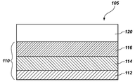
도 1b는 자기 재료 및 전도성 재료의 교번하는 부분들을 포함하는 자기 재료의 간략화된 단면도이다;
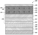
도 2 는 본 개시의 일 실시예에 따른 시드 재료를 포함한 자기 셀 구조의 간략화된 단면도이다 ;
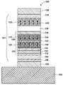
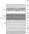
도 3은 본 개시의 다른 실시예에 따른 시드 재료를 포함한 자기 셀 구조의 간략화된 단면도이다 ;
도면들 4a 내지 도 4d는 도 2의 자기 셀 구조를 형성하는 방법의 실시예를 위한 상이한 프로세스 스테이지들을 예시하는 간략화된 단면도들이다;
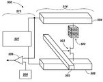
도 5는 본 개시의 실시예에 따른 자기 셀 구조를 갖는 메모리 셀을 포함하는 STT-MRAM 시스템의 개략도이다.
도 6 은 통상의 시드 재료를 포함하는 자기 구조에 비교된 백금-함유 시드 재료를 포함하는 자기 구조의 이방성 필드 (즉, Hk)를 비교한 평면내 루프 플롯(plot)이다 ;
도 7 은 300℃에서 각각의 구조들을 어닐링한 후에 통상의 시드 재료를 포함한 자기 셀 구조에 도 2 의 자기 셀 구조의 자기 특성들을 비교한 평면외 루프 플롯이다;
도 8a 는 300℃에서 각각의 구조들 어닐링에 이어 360℃에서 각각의 구조들 어닐링 한 후에 통상의 시드 재료를 포함한 자기 셀 구조에 도 2 의 자기 셀 구조의 자기 특성들을 비교한 평면외 루프 플롯이다;
도 8b는 300℃에서 각각의 구조들 어닐링에 이어 360℃에서 각각의 구조들 어닐링 한 후에 통상의 시드 재료를 포함한 자기 셀 구조에 도 2 의 자기 셀 구조의 자기 특성들을 비교한 평면내 루프 플롯이다;
도 9a는 아몰퍼스 기판 위에 성장된 자기 셀 구조의 자기 특성들에 결정질 기판 위에 성장된 자기 셀 구조의 자기 특성들을 비교한 평면외 루프 플롯이다; 및
도 9b는 각각의 자기 셀 구조들이 기판과 시드 재료 사이에 아몰퍼스 재료를 포함할 때 아몰퍼스 기판 위에 성장된 자기 셀 구조의 자기 특성들에 결정질 기판 위에 성장된 자기 셀 구조의 자기 특성들을 비교한 평면외 루프 플롯이다.
Claims (19)
- 반도체 디바이스에 있어서,
기판 위 전극 위에 놓인(overlying) 적어도 하나의 자기 셀 구조로서, 상기 적어도 하나의 자기 셀 구조는 :
상기 전극 위에 놓인 탄탈륨, 백금(platinum), 및 루테늄을 포함하는 시드 재료(seed material);
상기 시드 재료 위에 놓인 자기 영역;
상기 자기 영역 위에 놓인 절연 재료;
상기 절연 재료 위에 놓인 다른 자기 영역을 포함하는, 상기 적어도 하나의 자기 셀 구조; 및
상기 다른 자기 영역 위에 놓인 다른 전극을 포함하는, 반도체 디바이스. - 청구항 1에 있어서, 상기 적어도 하나의 자기 셀 구조는 자기 셀 구조들의 어레이를 포함하는, 반도체 디바이스.
- 청구항 1 또는 2에 있어서, 상기 시드 재료의 상기 백금은 상기 탄탈륨을 포함하는 상기 시드 재료의 영역과 상기 루테늄를 포함하는 상기 시드 재료의 다른 영역 사이에 배치된, 반도체 디바이스.
- 청구항 1 내지 청구항 3 중 어느 한 항에 있어서, 상기 자기 영역은 상기 시드 재료의 상기 루테늄의 바로 위에 놓인, 반도체 디바이스.
- 청구항 1 내지 청구항 4 어느 한 항에 있어서, 상기 자기 영역은 코발트 및 백금의 교번하는 부분들을 포함하는, 반도체 디바이스.
- 청구항 5에 있어서, 상기 코발트의 교번하는 부분들은 코발트의 약 1.0 Å과 약 6.0 Å 사이를 포함하는, 반도체 디바이스.
- 청구항 1 내지 청구항 6 중 어느 한 항에 있어서, 상기 시드 재료의 하지(underlying)에 니켈 및 코발트를 포함하는 아몰퍼스 영역을 더 포함하는, 반도체 디바이스.
- 청구항 7에 있어서, 상기 시드 재료의 상기 탄탈륨은 상기 아몰퍼스 영역을 컨택하는, 반도체 디바이스.
- 청구항 1 내지 청구항 8 중 어느 한 항에 있어서, 상기 다른 자기 영역은 백금, 팔라듐, 니켈, 및 이리듐의 적어도 하나와 코발트의 교번하는 부분들을 포함하는, 반도체 디바이스.
- 청구항 1 내지 청구항 9 중 어느 한 항에 있어서, 상기 자기 영역 및 상기 다른 자기 영역은 수직 자기 방위를 나타내는, 반도체 디바이스.
- 청구항 1 내지 청구항 10 중 어느 한 항에 있어서, 상기 자기 영역은 고정된 자기 방위를 나타내는, 반도체 디바이스.
- 청구항 1 내지 청구항 11 중 어느 한 항에 있어서, 상기 시드 재료는 약 10 Å과 약 1,000 Å 사이의 두께를 갖는 백금 부분을 포함하는, 반도체 디바이스.
- 청구항 12에 있어서, 상기 백금 부분은 약 90 원자 퍼센트와 약 100 원자 퍼센트 백금 사이를 포함하는, 반도체 디바이스.
- 청구항 1 내지 청구항 13 중 어느 한 항에 있어서, 상기 시드 재료는 상기 기판 위에 놓인 탄탈륨 부분, 상기 탄탈륨 부분 위에 놓인 백금 부분, 및 상기 백금 부분 위에 놓인 루테늄 부분을 포함하는, 반도체 디바이스.
- 반도체 디바이스를 형성하는 방법에 있어서, 상기 방법은:
기판상의 전극 위에 자기 셀 구조들의 어레이를 형성하는 단계로서, 상기 자기 셀 구조들의 어레이를 형성하는 단계는 :
상기 전극 위에 탄탈륨, 백금, 및 루테늄을 포함하는 시드 재료(seed material)를 형성하는 단계;
상기 시드 재료 위에 자기 재료를 형성하는 단계;
상기 자기 재료 위에 절연 재료를 형성하는 단계; 및
상기 절연 재료 위에 다른 자기 재료를 형성하는 단계;를 포함하는, 상기 자기 셀 구조들의 어레이를 형성하는 단계; 및
상기 어레이의 상기 자기 셀 구조의 각각의 상기 다른 자기 재료 위에 다른 전극을 형성하는 단계를 포함하는, 방법. - 청구항 15에 있어서, 약 한 시간 동안 약 360℃의 온도에서 상기 시드 재료 및 상기 자기 재료를 어닐링하는 단계를 더 포함하는, 방법.
- 청구항 15 또는 16에 있어서, 상기 기판과 상기 시드 재료 사이에 니켈 및 크롬을 포함하는 아몰퍼스 재료를 형성하는 단계를 더 포함하는, 방법.
- 청구항 15 내지 청구항 17 중 어느 한 항에 있어서, 상기 시드 재료 위에 자기 재료를 형성하는 단계는 상기 시드 재료 위에 고정된 자기 방위를 나타내는 자기 재료를 형성하는 단계를 포함하는, 방법.
- 청구항 15 내지 청구항 18 중 어느 한 항에 있어서, 상기 전극 위에 탄탈륨, 백금, 및 루테늄을 포함하는 시드 재료를 형성하는 단계는:
상기 기판 위에 탄탈륨을 형성하는 단계;
상기 탄탈륨 위에 루테늄을 형성하는 단계; 및
상기 탄탈륨과 상기 루테늄 사이에 백금을 형성하는 단계를 포함하는, 방법.
Applications Claiming Priority (3)
| Application Number | Priority Date | Filing Date | Title |
|---|---|---|---|
| US14/558,367 | 2014-12-02 | ||
| US14/558,367 US9768377B2 (en) | 2014-12-02 | 2014-12-02 | Magnetic cell structures, and methods of fabrication |
| PCT/US2015/062453 WO2016089682A1 (en) | 2014-12-02 | 2015-11-24 | Magnetic cell structures, and methods of fabrication |
Publications (2)
| Publication Number | Publication Date |
|---|---|
| KR20170091691A true KR20170091691A (ko) | 2017-08-09 |
| KR102051194B1 KR102051194B1 (ko) | 2020-01-08 |
Family
ID=56079699
Family Applications (1)
| Application Number | Title | Priority Date | Filing Date |
|---|---|---|---|
| KR1020177017984A Active KR102051194B1 (ko) | 2014-12-02 | 2015-11-24 | 자기 셀 구조들, 및 제조 방법들 |
Country Status (7)
| Country | Link |
|---|---|
| US (2) | US9768377B2 (ko) |
| EP (1) | EP3227931B1 (ko) |
| JP (1) | JP6464516B2 (ko) |
| KR (1) | KR102051194B1 (ko) |
| CN (1) | CN107004764B (ko) |
| TW (1) | TWI596808B (ko) |
| WO (1) | WO2016089682A1 (ko) |
Cited By (3)
| Publication number | Priority date | Publication date | Assignee | Title |
|---|---|---|---|---|
| KR20190142201A (ko) * | 2018-06-15 | 2019-12-26 | 인텔 코포레이션 | 개선된 보유 및 열 안정성을 갖는 수직 스핀 전달 토크 디바이스 |
| CN110660905A (zh) * | 2018-06-29 | 2020-01-07 | 台湾积体电路制造股份有限公司 | 半导体器件、mram器件和制造存储器器件的方法 |
| KR20210019122A (ko) * | 2018-07-09 | 2021-02-19 | 어플라이드 머티어리얼스, 인코포레이티드 | 자기 터널 접합들 및 그의 제조 방법들 |
Families Citing this family (30)
| Publication number | Priority date | Publication date | Assignee | Title |
|---|---|---|---|---|
| US9368714B2 (en) | 2013-07-01 | 2016-06-14 | Micron Technology, Inc. | Memory cells, methods of operation and fabrication, semiconductor device structures, and memory systems |
| US9461242B2 (en) | 2013-09-13 | 2016-10-04 | Micron Technology, Inc. | Magnetic memory cells, methods of fabrication, semiconductor devices, memory systems, and electronic systems |
| US9608197B2 (en) | 2013-09-18 | 2017-03-28 | Micron Technology, Inc. | Memory cells, methods of fabrication, and semiconductor devices |
| US10454024B2 (en) | 2014-02-28 | 2019-10-22 | Micron Technology, Inc. | Memory cells, methods of fabrication, and memory devices |
| US9281466B2 (en) | 2014-04-09 | 2016-03-08 | Micron Technology, Inc. | Memory cells, semiconductor structures, semiconductor devices, and methods of fabrication |
| US9269888B2 (en) * | 2014-04-18 | 2016-02-23 | Micron Technology, Inc. | Memory cells, methods of fabrication, and semiconductor devices |
| US9349945B2 (en) | 2014-10-16 | 2016-05-24 | Micron Technology, Inc. | Memory cells, semiconductor devices, and methods of fabrication |
| US9768377B2 (en) | 2014-12-02 | 2017-09-19 | Micron Technology, Inc. | Magnetic cell structures, and methods of fabrication |
| US10439131B2 (en) | 2015-01-15 | 2019-10-08 | Micron Technology, Inc. | Methods of forming semiconductor devices including tunnel barrier materials |
| US10483320B2 (en) | 2015-12-10 | 2019-11-19 | Everspin Technologies, Inc. | Magnetoresistive stack with seed region and method of manufacturing the same |
| US10559748B2 (en) * | 2016-02-19 | 2020-02-11 | Tohoku University | Tunnel magnetic resistance element and method for manufacturing same |
| US10103196B2 (en) | 2016-08-30 | 2018-10-16 | Micron Technology, Inc. | Methods of forming magnetic memory cells, and methods of forming arrays of magnetic memory cells |
| US10014345B1 (en) | 2017-01-05 | 2018-07-03 | Micron Technology, Inc. | Magnetic memory device with grid-shaped common source plate, system, and method of fabrication |
| US10453895B2 (en) | 2017-01-05 | 2019-10-22 | Micron Technology, Inc. | Magnetic memory device with a common source having an array of openings, system, and method of fabrication |
| US10727271B2 (en) | 2017-01-05 | 2020-07-28 | Micron Trechnology, Inc. | Memory device having source contacts located at intersections of linear portions of a common source, electronic systems, and associated methods |
| US10446175B2 (en) * | 2017-05-16 | 2019-10-15 | Western Digital Technologies, Inc. | Spin transfer torque device with oxide layer beneath the seed layer |
| US10734013B2 (en) | 2017-10-03 | 2020-08-04 | Western Digital Technologies, Inc. | Spin transfer torque (STT) device with multilayer seed layers for magnetic recording and memory |
| US10388853B2 (en) * | 2017-12-29 | 2019-08-20 | Spin Memory, Inc. | Magnetic memory having a pinning synthetic antiferromagnetic structure (SAF) with cobalt over platinum (Pt/Co) bilayers |
| JP2019164848A (ja) * | 2018-03-19 | 2019-09-26 | 東芝メモリ株式会社 | 磁気記憶装置 |
| US10957849B2 (en) * | 2018-05-24 | 2021-03-23 | Applied Materials, Inc. | Magnetic tunnel junctions with coupling-pinning layer lattice matching |
| US11502188B2 (en) | 2018-06-14 | 2022-11-15 | Intel Corporation | Apparatus and method for boosting signal in magnetoelectric spin orbit logic |
| US11476412B2 (en) | 2018-06-19 | 2022-10-18 | Intel Corporation | Perpendicular exchange bias with antiferromagnet for spin orbit coupling based memory |
| US11770979B2 (en) * | 2018-06-29 | 2023-09-26 | Intel Corporation | Conductive alloy layer in magnetic memory devices and methods of fabrication |
| US11616192B2 (en) | 2018-06-29 | 2023-03-28 | Intel Corporation | Magnetic memory devices with a transition metal dopant at an interface of free magnetic layers and methods of fabrication |
| US12052927B2 (en) | 2018-08-23 | 2024-07-30 | Everspin Technologies, Inc. | Magnetoresistive stack device fabrication methods |
| WO2020106552A1 (en) * | 2018-11-19 | 2020-05-28 | Everspin Technologies, Inc. | Magnetoresistive stack with seed region and method of manufacturing the same |
| JP2020155565A (ja) | 2019-03-20 | 2020-09-24 | キオクシア株式会社 | 磁気記憶装置 |
| US12075629B2 (en) | 2019-03-20 | 2024-08-27 | Kioxia Corporation | Magnetic memory device with nonmagnetic layer having two additive elements |
| CN112652704A (zh) * | 2019-10-10 | 2021-04-13 | 上海磁宇信息科技有限公司 | 具有超薄合成反铁磁层的磁性隧道结单元 |
| JP7518524B2 (ja) * | 2020-03-13 | 2024-07-18 | 国立大学法人京都大学 | 磁気メモリ素子 |
Citations (6)
| Publication number | Priority date | Publication date | Assignee | Title |
|---|---|---|---|---|
| JP2007035139A (ja) * | 2005-07-26 | 2007-02-08 | Hitachi Global Storage Technologies Netherlands Bv | 垂直磁気記録媒体及び磁気記録再生装置 |
| WO2010137679A1 (ja) * | 2009-05-28 | 2010-12-02 | 株式会社日立製作所 | 磁気抵抗効果素子及びそれを用いたランダムアクセスメモリ |
| JP2011521391A (ja) * | 2008-05-06 | 2011-07-21 | コミッサリア ア レネルジー アトミーク エ オ ゼネルジ ザルタナテイヴ | 熱アシスト磁気書き込み素子 |
| KR20120009926A (ko) * | 2010-07-22 | 2012-02-02 | 삼성전자주식회사 | 자기 메모리 소자 및 이를 포함하는 메모리 카드 및 시스템 |
| US20130148418A1 (en) * | 2011-12-07 | 2013-06-13 | Agency For Science, Technology And Research | Magnetoresistive device and a writing method for a magnetoresistive device |
| KR20140135002A (ko) * | 2013-05-15 | 2014-11-25 | 삼성전자주식회사 | 자기 기억 소자 및 그 제조방법 |
Family Cites Families (329)
| Publication number | Priority date | Publication date | Assignee | Title |
|---|---|---|---|---|
| US4760745A (en) | 1986-12-05 | 1988-08-02 | Mag Dev Inc. | Magnetoelastic torque transducer |
| DE69117350T2 (de) * | 1990-05-29 | 1996-10-10 | Oki Electric Ind Co Ltd | Verfahren zur Herstellung magnetischer Aufzeichnungsträger |
| US5565266A (en) * | 1993-06-14 | 1996-10-15 | Eastman Kodak Company | Multilayer magnetooptic recording media |
| JP3260921B2 (ja) * | 1993-08-25 | 2002-02-25 | 株式会社デンソー | 可動体変位検出装置 |
| US5563000A (en) * | 1994-03-11 | 1996-10-08 | Eastman Kodak Company | Multilayer magnetooptic recording media |
| US5583725A (en) * | 1994-06-15 | 1996-12-10 | International Business Machines Corporation | Spin valve magnetoresistive sensor with self-pinned laminated layer and magnetic recording system using the sensor |
| US5768069A (en) | 1996-11-27 | 1998-06-16 | International Business Machines Corporation | Self-biased dual spin valve sensor |
| US6256224B1 (en) | 2000-05-03 | 2001-07-03 | Hewlett-Packard Co | Write circuit for large MRAM arrays |
| US6468856B2 (en) | 1997-07-24 | 2002-10-22 | Texas Instruments Incorporated | High charge storage density integrated circuit capacitor |
| US6258470B1 (en) | 1998-01-16 | 2001-07-10 | Matsushita Electric Industrial Co., Ltd. | Exchange coupling film, magnetoresistance effect device, magnetoresistance effective head and method for producing exchange coupling film |
| JP2000020937A (ja) * | 1998-07-03 | 2000-01-21 | Hitachi Ltd | 磁気記録媒体およびこれを用いた磁気記憶装置 |
| GB2343308B (en) | 1998-10-30 | 2000-10-11 | Nikolai Franz Gregor Schwabe | Magnetic storage device |
| JP4568926B2 (ja) | 1999-07-14 | 2010-10-27 | ソニー株式会社 | 磁気機能素子及び磁気記録装置 |
| US6275363B1 (en) | 1999-07-23 | 2001-08-14 | International Business Machines Corporation | Read head with dual tunnel junction sensor |
| US6166948A (en) | 1999-09-03 | 2000-12-26 | International Business Machines Corporation | Magnetic memory array with magnetic tunnel junction memory cells having flux-closed free layers |
| US6611405B1 (en) | 1999-09-16 | 2003-08-26 | Kabushiki Kaisha Toshiba | Magnetoresistive element and magnetic memory device |
| JP2001084756A (ja) | 1999-09-17 | 2001-03-30 | Sony Corp | 磁化駆動方法、磁気機能素子および磁気装置 |
| US6979586B2 (en) | 2000-10-06 | 2005-12-27 | Headway Technologies, Inc. | Magnetic random access memory array with coupled soft adjacent magnetic layer |
| US6710987B2 (en) | 2000-11-17 | 2004-03-23 | Tdk Corporation | Magnetic tunnel junction read head devices having a tunneling barrier formed by multi-layer, multi-oxidation processes |
| FR2817999B1 (fr) | 2000-12-07 | 2003-01-10 | Commissariat Energie Atomique | Dispositif magnetique a polarisation de spin et a empilement(s) tri-couche(s) et memoire utilisant ce dispositif |
| US6955857B2 (en) * | 2000-12-29 | 2005-10-18 | Seagate Technology Llc | Exchange decoupled cobalt/noble metal perpendicular recording media |
| US6603678B2 (en) | 2001-01-11 | 2003-08-05 | Hewlett-Packard Development Company, L.P. | Thermally-assisted switching of magnetic memory elements |
| JP2002208682A (ja) | 2001-01-12 | 2002-07-26 | Hitachi Ltd | 磁気半導体記憶装置及びその製造方法 |
| JP2002314164A (ja) | 2001-02-06 | 2002-10-25 | Sony Corp | 磁気トンネル素子及びその製造方法、薄膜磁気ヘッド、磁気メモリ、並びに磁気センサ |
| JP2002314049A (ja) | 2001-04-18 | 2002-10-25 | Nec Corp | 磁性メモリ及びその製造方法 |
| JP2004179668A (ja) | 2001-05-15 | 2004-06-24 | Matsushita Electric Ind Co Ltd | 磁気抵抗素子 |
| US7220498B2 (en) | 2001-05-31 | 2007-05-22 | National Institute Of Advanced Industrial Science And Technology | Tunnel magnetoresistance element |
| US6667861B2 (en) | 2001-07-16 | 2003-12-23 | International Business Machines Corporation | Dual/differential GMR head with a single AFM layer |
| JP4198900B2 (ja) * | 2001-07-19 | 2008-12-17 | アルプス電気株式会社 | 交換結合膜及び前記交換結合膜を用いた磁気検出素子 |
| JP4189146B2 (ja) * | 2001-07-19 | 2008-12-03 | アルプス電気株式会社 | 交換結合膜及び前記交換結合膜を用いた磁気検出素子 |
| JP2003031870A (ja) * | 2001-07-19 | 2003-01-31 | Alps Electric Co Ltd | 交換結合膜及び前記交換結合膜を用いた磁気検出素子 |
| US6347049B1 (en) | 2001-07-25 | 2002-02-12 | International Business Machines Corporation | Low resistance magnetic tunnel junction device with bilayer or multilayer tunnel barrier |
| TW554398B (en) | 2001-08-10 | 2003-09-21 | Semiconductor Energy Lab | Method of peeling off and method of manufacturing semiconductor device |
| US6805710B2 (en) | 2001-11-13 | 2004-10-19 | Edwards Lifesciences Corporation | Mitral valve annuloplasty ring for molding left ventricle geometry |
| US6829157B2 (en) | 2001-12-05 | 2004-12-07 | Korea Institute Of Science And Technology | Method of controlling magnetization easy axis in ferromagnetic films using voltage, ultrahigh-density, low power, nonvolatile magnetic memory using the control method, and method of writing information on the magnetic memory |
| US7095933B2 (en) | 2002-04-09 | 2006-08-22 | Barth Phillip W | Systems and methods for designing and fabricating multi-layer structures having thermal expansion properties |
| US6866255B2 (en) | 2002-04-12 | 2005-03-15 | Xerox Corporation | Sputtered spring films with low stress anisotropy |
| US6815248B2 (en) | 2002-04-18 | 2004-11-09 | Infineon Technologies Ag | Material combinations for tunnel junction cap layer, tunnel junction hard mask and tunnel junction stack seed layer in MRAM processing |
| JP2003332649A (ja) * | 2002-05-14 | 2003-11-21 | Alps Electric Co Ltd | 磁気検出素子 |
| US6849464B2 (en) | 2002-06-10 | 2005-02-01 | Micron Technology, Inc. | Method of fabricating a multilayer dielectric tunnel barrier structure |
| JP3678213B2 (ja) | 2002-06-20 | 2005-08-03 | ソニー株式会社 | 磁気抵抗効果素子及び磁気メモリ装置、磁気抵抗効果素子及び磁気メモリ装置の製造方法 |
| JP4252353B2 (ja) | 2002-07-16 | 2009-04-08 | 株式会社日立製作所 | 半導体レーザ素子の製造方法 |
| US6653704B1 (en) * | 2002-09-24 | 2003-11-25 | International Business Machines Corporation | Magnetic memory with tunnel junction memory cells and phase transition material for controlling current to the cells |
| JP2004128229A (ja) | 2002-10-02 | 2004-04-22 | Nec Corp | 磁性メモリ及びその製造方法 |
| US6985338B2 (en) | 2002-10-21 | 2006-01-10 | International Business Machines Corporation | Insulative in-stack hard bias for GMR sensor stabilization |
| US6980468B1 (en) | 2002-10-28 | 2005-12-27 | Silicon Magnetic Systems | High density MRAM using thermal writing |
| US7394626B2 (en) | 2002-11-01 | 2008-07-01 | Nec Corporation | Magnetoresistance device with a diffusion barrier between a conductor and a magnetoresistance element and method of fabricating the same |
| US6756128B2 (en) | 2002-11-07 | 2004-06-29 | International Business Machines Corporation | Low-resistance high-magnetoresistance magnetic tunnel junction device with improved tunnel barrier |
| US6771534B2 (en) | 2002-11-15 | 2004-08-03 | International Business Machines Corporation | Thermally-assisted magnetic writing using an oxide layer and current-induced heating |
| US6841395B2 (en) | 2002-11-25 | 2005-01-11 | International Business Machines Corporation | Method of forming a barrier layer of a tunneling magnetoresistive sensor |
| JP2004200245A (ja) | 2002-12-16 | 2004-07-15 | Nec Corp | 磁気抵抗素子及び磁気抵抗素子の製造方法 |
| US6845038B1 (en) | 2003-02-01 | 2005-01-18 | Alla Mikhailovna Shukh | Magnetic tunnel junction memory device |
| US6952364B2 (en) | 2003-03-03 | 2005-10-04 | Samsung Electronics Co., Ltd. | Magnetic tunnel junction structures and methods of fabrication |
| US6998150B2 (en) | 2003-03-12 | 2006-02-14 | Headway Technologies, Inc. | Method of adjusting CoFe free layer magnetostriction |
| KR100544690B1 (ko) | 2003-04-25 | 2006-01-24 | 재단법인서울대학교산학협력재단 | 비휘발성 자기 메모리 셀, 동작 방법 및 이를 이용한다진법 비휘발성 초고집적 자기 메모리 |
| US6964819B1 (en) * | 2003-05-06 | 2005-11-15 | Seagate Technology Llc | Anti-ferromagnetically coupled recording media with enhanced RKKY coupling |
| US20040224243A1 (en) | 2003-05-08 | 2004-11-11 | Sony Corporation | Mask, mask blank, and methods of producing these |
| US6865109B2 (en) | 2003-06-06 | 2005-03-08 | Seagate Technology Llc | Magnetic random access memory having flux closure for the free layer and spin transfer write mechanism |
| US6806096B1 (en) | 2003-06-18 | 2004-10-19 | Infineon Technologies Ag | Integration scheme for avoiding plasma damage in MRAM technology |
| US7189583B2 (en) | 2003-07-02 | 2007-03-13 | Micron Technology, Inc. | Method for production of MRAM elements |
| JP4169663B2 (ja) | 2003-07-25 | 2008-10-22 | Hoya株式会社 | 垂直磁気記録媒体 |
| US7092220B2 (en) * | 2003-07-29 | 2006-08-15 | Hitachi Global Storage Technologies | Apparatus for enhancing thermal stability, improving biasing and reducing damage from electrostatic discharge in self-pinned abutted junction heads having a first self-pinned layer extending under the hard bias layers |
| US7282277B2 (en) * | 2004-04-20 | 2007-10-16 | Seagate Technology Llc | Magnetic recording media with Cu-containing magnetic layers |
| KR100548997B1 (ko) | 2003-08-12 | 2006-02-02 | 삼성전자주식회사 | 다층박막구조의 자유층을 갖는 자기터널 접합 구조체들 및이를 채택하는 자기 램 셀들 |
| JP2005064050A (ja) | 2003-08-14 | 2005-03-10 | Toshiba Corp | 半導体記憶装置及びそのデータ書き込み方法 |
| US7274080B1 (en) | 2003-08-22 | 2007-09-25 | International Business Machines Corporation | MgO-based tunnel spin injectors |
| US7298595B2 (en) | 2003-09-26 | 2007-11-20 | Hitachi Global Storage Technologies Netherlands B.V. | Differential GMR sensor with multi-layer bias structure between free layers of first and second self-pinned GMR sensors |
| US7195927B2 (en) | 2003-10-22 | 2007-03-27 | Hewlett-Packard Development Company, L.P. | Process for making magnetic memory structures having different-sized memory cell layers |
| US7282755B2 (en) | 2003-11-14 | 2007-10-16 | Grandis, Inc. | Stress assisted current driven switching for magnetic memory applications |
| US7105372B2 (en) | 2004-01-20 | 2006-09-12 | Headway Technologies, Inc. | Magnetic tunneling junction film structure with process determined in-plane magnetic anisotropy |
| US7083988B2 (en) | 2004-01-26 | 2006-08-01 | Micron Technology, Inc. | Magnetic annealing sequences for patterned MRAM synthetic antiferromagnetic pinned layers |
| US7564152B1 (en) | 2004-02-12 | 2009-07-21 | The United States Of America As Represented By The Secretary Of The Navy | High magnetostriction of positive magnetostrictive materials under tensile load |
| US6992359B2 (en) | 2004-02-26 | 2006-01-31 | Grandis, Inc. | Spin transfer magnetic element with free layers having high perpendicular anisotropy and in-plane equilibrium magnetization |
| US7130167B2 (en) | 2004-03-03 | 2006-10-31 | Hitachi Global Storage Technologies Netherlands B.V. | Magnetoresistive sensor having improved synthetic free layer |
| JP2005251990A (ja) | 2004-03-04 | 2005-09-15 | Nec Electronics Corp | 不揮発性半導体記憶装置 |
| US20050211973A1 (en) | 2004-03-23 | 2005-09-29 | Kiyotaka Mori | Stressed organic semiconductor |
| US20070035890A1 (en) | 2004-04-02 | 2007-02-15 | Tdk Corporation | Composed free layer for stabilizing magnetoresistive head having low magnetostriction |
| US7190557B2 (en) | 2004-04-14 | 2007-03-13 | Hitachi Global Storage Technologies Netherlands B.V. | Current-in-the-plane spin valve magnetoresistive sensor with dual metal oxide capping layers |
| JP3863536B2 (ja) | 2004-05-17 | 2006-12-27 | 株式会社東芝 | 磁気ランダムアクセスメモリ及びその磁気ランダムアクセスメモリのデータ書き込み方法 |
| US7449345B2 (en) * | 2004-06-15 | 2008-11-11 | Headway Technologies, Inc. | Capping structure for enhancing dR/R of the MTJ device |
| JP2006005286A (ja) * | 2004-06-21 | 2006-01-05 | Alps Electric Co Ltd | 磁気検出素子 |
| JP4868198B2 (ja) | 2004-08-19 | 2012-02-01 | 日本電気株式会社 | 磁性メモリ |
| US20060042930A1 (en) | 2004-08-26 | 2006-03-02 | Daniele Mauri | Method for reactive sputter deposition of a magnesium oxide (MgO) tunnel barrier in a magnetic tunnel junction |
| US7355884B2 (en) | 2004-10-08 | 2008-04-08 | Kabushiki Kaisha Toshiba | Magnetoresistive element |
| US7351483B2 (en) | 2004-11-10 | 2008-04-01 | International Business Machines Corporation | Magnetic tunnel junctions using amorphous materials as reference and free layers |
| JP5093747B2 (ja) | 2004-11-16 | 2012-12-12 | 日本電気株式会社 | 磁気メモリ |
| JP2006156608A (ja) | 2004-11-29 | 2006-06-15 | Hitachi Ltd | 磁気メモリおよびその製造方法 |
| JP2006165059A (ja) | 2004-12-02 | 2006-06-22 | Sony Corp | 記憶素子及びメモリ |
| JP2006165327A (ja) | 2004-12-08 | 2006-06-22 | Toshiba Corp | 磁気ランダムアクセスメモリ |
| JP5077802B2 (ja) | 2005-02-16 | 2012-11-21 | 日本電気株式会社 | 積層強磁性構造体、及び、mtj素子 |
| US7230265B2 (en) | 2005-05-16 | 2007-06-12 | International Business Machines Corporation | Spin-polarization devices using rare earth-transition metal alloys |
| US8068317B2 (en) | 2005-07-22 | 2011-11-29 | Hitachi Global Storage Technologies Netherlands B.V. | Magnetic tunnel transistor with high magnetocurrent |
| US7372674B2 (en) | 2005-07-22 | 2008-05-13 | Hitachi Global Storage Technologies Netherlands B.V. | Magnetic tunnel transistor with high magnetocurrent and stronger pinning |
| US7862914B2 (en) * | 2005-07-26 | 2011-01-04 | Seagate Technology Llc | Heatsink films for magnetic recording media |
| US7349187B2 (en) | 2005-09-07 | 2008-03-25 | International Business Machines Corporation | Tunnel barriers based on alkaline earth oxides |
| FR2892231B1 (fr) | 2005-10-14 | 2008-06-27 | Commissariat Energie Atomique | Dispositif magnetique a jonction tunnel magnetoresistive et memoire magnetique a acces aleatoire |
| JP4444241B2 (ja) | 2005-10-19 | 2010-03-31 | 株式会社東芝 | 磁気抵抗効果素子、磁気ランダムアクセスメモリ、電子カード及び電子装置 |
| JP4768427B2 (ja) | 2005-12-12 | 2011-09-07 | 株式会社東芝 | 半導体記憶装置 |
| US7791844B2 (en) | 2005-12-14 | 2010-09-07 | Hitachi Global Storage Technologies Netherlands B.V. | Magnetoresistive sensor having a magnetically stable free layer with a positive magnetostriction |
| JP4786331B2 (ja) | 2005-12-21 | 2011-10-05 | 株式会社東芝 | 磁気抵抗効果素子の製造方法 |
| US7479394B2 (en) | 2005-12-22 | 2009-01-20 | Magic Technologies, Inc. | MgO/NiFe MTJ for high performance MRAM application |
| US8058696B2 (en) | 2006-02-25 | 2011-11-15 | Avalanche Technology, Inc. | High capacity low cost multi-state magnetic memory |
| US7732881B2 (en) | 2006-11-01 | 2010-06-08 | Avalanche Technology, Inc. | Current-confined effect of magnetic nano-current-channel (NCC) for magnetic random access memory (MRAM) |
| US8508984B2 (en) | 2006-02-25 | 2013-08-13 | Avalanche Technology, Inc. | Low resistance high-TMR magnetic tunnel junction and process for fabrication thereof |
| CN101615653B (zh) | 2006-03-03 | 2012-07-18 | 佳能安内华股份有限公司 | 磁阻效应元件的制造方法以及制造设备 |
| JP2007250094A (ja) | 2006-03-16 | 2007-09-27 | Fujitsu Ltd | 磁気記録媒体、磁気記録媒体の製造方法、及び磁気記録装置 |
| JP2007273504A (ja) * | 2006-03-30 | 2007-10-18 | Fujitsu Ltd | 磁気抵抗効果素子、磁気ヘッド、磁気記録装置、磁気ランダムアクセスメモリ |
| TWI309411B (en) * | 2006-04-21 | 2009-05-01 | Nat Univ Tsing Hua | Perpendicular magnetic recording media |
| US8120949B2 (en) | 2006-04-27 | 2012-02-21 | Avalanche Technology, Inc. | Low-cost non-volatile flash-RAM memory |
| JP4731393B2 (ja) | 2006-04-28 | 2011-07-20 | 株式会社日立製作所 | 磁気再生ヘッド |
| US7486550B2 (en) | 2006-06-06 | 2009-02-03 | Micron Technology, Inc. | Semiconductor magnetic memory integrating a magnetic tunneling junction above a floating-gate memory cell |
| US20070297220A1 (en) | 2006-06-22 | 2007-12-27 | Masatoshi Yoshikawa | Magnetoresistive element and magnetic memory |
| JP2008010590A (ja) * | 2006-06-28 | 2008-01-17 | Toshiba Corp | 磁気抵抗素子及び磁気メモリ |
| US7595520B2 (en) | 2006-07-31 | 2009-09-29 | Magic Technologies, Inc. | Capping layer for a magnetic tunnel junction device to enhance dR/R and a method of making the same |
| JP4496189B2 (ja) | 2006-09-28 | 2010-07-07 | 株式会社東芝 | 磁気抵抗効果型素子および磁気抵抗効果型ランダムアクセスメモリ |
| JP2008098523A (ja) | 2006-10-13 | 2008-04-24 | Toshiba Corp | 磁気抵抗効果素子および磁気メモリ |
| US20080170329A1 (en) * | 2007-01-11 | 2008-07-17 | Seagate Technology Llc | Granular perpendicular magnetic recording media with improved corrosion resistance by SUL post-deposition heating |
| JP4751344B2 (ja) | 2007-01-26 | 2011-08-17 | 株式会社東芝 | 垂直磁気記録媒体、及び磁気記録再生装置 |
| US7598579B2 (en) | 2007-01-30 | 2009-10-06 | Magic Technologies, Inc. | Magnetic tunnel junction (MTJ) to reduce spin transfer magnetization switching current |
| JP2010518536A (ja) * | 2007-02-03 | 2010-05-27 | ダブリューディー メディア インコーポレイテッド | 改良された異方性磁界を有する垂直磁気記録媒体 |
| JP2008192926A (ja) | 2007-02-06 | 2008-08-21 | Tdk Corp | トンネル型磁気検出素子及びその製造方法 |
| US8593862B2 (en) | 2007-02-12 | 2013-11-26 | Avalanche Technology, Inc. | Spin-transfer torque magnetic random access memory having magnetic tunnel junction with perpendicular magnetic anisotropy |
| US8623452B2 (en) | 2010-12-10 | 2014-01-07 | Avalanche Technology, Inc. | Magnetic random access memory (MRAM) with enhanced magnetic stiffness and method of making same |
| US20090218645A1 (en) | 2007-02-12 | 2009-09-03 | Yadav Technology Inc. | multi-state spin-torque transfer magnetic random access memory |
| JP5143444B2 (ja) | 2007-02-13 | 2013-02-13 | 株式会社日立製作所 | 磁気抵抗効果素子、それを用いた磁気メモリセル及び磁気ランダムアクセスメモリ |
| JP2008204539A (ja) * | 2007-02-20 | 2008-09-04 | Fujitsu Ltd | 垂直磁気記録媒体およびその製造方法、磁気記録装置 |
| US20080205130A1 (en) | 2007-02-28 | 2008-08-28 | Freescale Semiconductor, Inc. | Mram free layer synthetic antiferromagnet structure and methods |
| JP4682998B2 (ja) | 2007-03-15 | 2011-05-11 | ソニー株式会社 | 記憶素子及びメモリ |
| US20080242088A1 (en) | 2007-03-29 | 2008-10-02 | Tokyo Electron Limited | Method of forming low resistivity copper film structures |
| JP2008263031A (ja) | 2007-04-11 | 2008-10-30 | Toshiba Corp | 磁気抵抗効果素子とその製造方法、磁気抵抗効果素子を備えた磁気記憶装置とその製造方法 |
| US8097175B2 (en) | 2008-10-28 | 2012-01-17 | Micron Technology, Inc. | Method for selectively permeating a self-assembled block copolymer, method for forming metal oxide structures, method for forming a metal oxide pattern, and method for patterning a semiconductor structure |
| US7682841B2 (en) | 2007-05-02 | 2010-03-23 | Qimonda Ag | Method of forming integrated circuit having a magnetic tunnel junction device |
| US7486552B2 (en) | 2007-05-21 | 2009-02-03 | Grandis, Inc. | Method and system for providing a spin transfer device with improved switching characteristics |
| US7602033B2 (en) | 2007-05-29 | 2009-10-13 | Headway Technologies, Inc. | Low resistance tunneling magnetoresistive sensor with composite inner pinned layer |
| EP2015307B8 (en) | 2007-07-13 | 2013-05-15 | Hitachi Ltd. | Magnetoresistive device |
| US7750421B2 (en) | 2007-07-23 | 2010-07-06 | Magic Technologies, Inc. | High performance MTJ element for STT-RAM and method for making the same |
| TW200907964A (en) | 2007-08-09 | 2009-02-16 | Ind Tech Res Inst | Structure of magnetic memory cell and magnetic memory device |
| JP5397926B2 (ja) | 2007-08-31 | 2014-01-22 | 昭和電工株式会社 | 垂直磁気記録媒体、その製造方法および磁気記録再生装置 |
| JP4649457B2 (ja) * | 2007-09-26 | 2011-03-09 | 株式会社東芝 | 磁気抵抗素子及び磁気メモリ |
| US8497559B2 (en) | 2007-10-10 | 2013-07-30 | Magic Technologies, Inc. | MRAM with means of controlling magnetic anisotropy |
| US8372661B2 (en) | 2007-10-31 | 2013-02-12 | Magic Technologies, Inc. | High performance MTJ element for conventional MRAM and for STT-RAM and a method for making the same |
| JP2009116930A (ja) * | 2007-11-02 | 2009-05-28 | Hitachi Global Storage Technologies Netherlands Bv | 垂直磁気記録媒体およびそれを用いた磁気記録再生装置 |
| US7488609B1 (en) | 2007-11-16 | 2009-02-10 | Hitachi Global Storage Technologies Netherlands B.V. | Method for forming an MgO barrier layer in a tunneling magnetoresistive (TMR) device |
| KR20090074396A (ko) * | 2008-01-02 | 2009-07-07 | 삼성전자주식회사 | 강유전체를 이용한 정보저장매체, 그 제조방법, 및 이를채용한 정보저장장치 |
| US7919794B2 (en) | 2008-01-08 | 2011-04-05 | Qualcomm, Incorporated | Memory cell and method of forming a magnetic tunnel junction (MTJ) of a memory cell |
| JP4703660B2 (ja) | 2008-01-11 | 2011-06-15 | 株式会社東芝 | スピンmos電界効果トランジスタ |
| JP5150284B2 (ja) | 2008-01-30 | 2013-02-20 | 株式会社東芝 | 磁気抵抗効果素子およびその製造方法 |
| US7727834B2 (en) | 2008-02-14 | 2010-06-01 | Toshiba America Electronic Components, Inc. | Contact configuration and method in dual-stress liner semiconductor device |
| JP2009194210A (ja) | 2008-02-15 | 2009-08-27 | Renesas Technology Corp | 半導体装置及び半導体装置の製造方法 |
| US8545999B1 (en) | 2008-02-21 | 2013-10-01 | Western Digital (Fremont), Llc | Method and system for providing a magnetoresistive structure |
| CN101960631B (zh) | 2008-03-07 | 2013-05-01 | 佳能安内华股份有限公司 | 制造磁阻元件的制造方法和磁阻元件的制造设备 |
| US9021685B2 (en) | 2008-03-12 | 2015-05-05 | Headway Technologies, Inc. | Two step annealing process for TMR device with amorphous free layer |
| JP4724196B2 (ja) | 2008-03-25 | 2011-07-13 | 株式会社東芝 | 磁気抵抗効果素子及び磁気ランダムアクセスメモリ |
| US7885105B2 (en) | 2008-03-25 | 2011-02-08 | Qualcomm Incorporated | Magnetic tunnel junction cell including multiple vertical magnetic domains |
| US8057925B2 (en) | 2008-03-27 | 2011-11-15 | Magic Technologies, Inc. | Low switching current dual spin filter (DSF) element for STT-RAM and a method for making the same |
| US8164862B2 (en) | 2008-04-02 | 2012-04-24 | Headway Technologies, Inc. | Seed layer for TMR or CPP-GMR sensor |
| JP2009252878A (ja) | 2008-04-03 | 2009-10-29 | Renesas Technology Corp | 磁気記憶装置 |
| US7948044B2 (en) * | 2008-04-09 | 2011-05-24 | Magic Technologies, Inc. | Low switching current MTJ element for ultra-high STT-RAM and a method for making the same |
| JP4774082B2 (ja) | 2008-06-23 | 2011-09-14 | キヤノンアネルバ株式会社 | 磁気抵抗効果素子の製造方法 |
| US8274818B2 (en) | 2008-08-05 | 2012-09-25 | Tohoku University | Magnetoresistive element, magnetic memory cell and magnetic random access memory using the same |
| JP5182631B2 (ja) | 2008-09-02 | 2013-04-17 | 富士電機株式会社 | 垂直磁気記録媒体 |
| US8803263B2 (en) | 2008-09-03 | 2014-08-12 | Fuji Electric Co., Ltd. | Magnetic memory element and storage device using the same |
| KR101004506B1 (ko) | 2008-09-09 | 2010-12-31 | 주식회사 하이닉스반도체 | 공통 소스라인을 갖는 수직 자기형 비휘발성 메모리 장치 및 그 제조 방법 |
| US8138561B2 (en) | 2008-09-18 | 2012-03-20 | Magic Technologies, Inc. | Structure and method to fabricate high performance MTJ devices for spin-transfer torque (STT)-RAM |
| US7940551B2 (en) | 2008-09-29 | 2011-05-10 | Seagate Technology, Llc | STRAM with electronically reflective insulative spacer |
| US8102700B2 (en) | 2008-09-30 | 2012-01-24 | Micron Technology, Inc. | Unidirectional spin torque transfer magnetic memory cell structure |
| US8310861B2 (en) | 2008-09-30 | 2012-11-13 | Micron Technology, Inc. | STT-MRAM cell structure incorporating piezoelectric stress material |
| JP2010087355A (ja) | 2008-10-01 | 2010-04-15 | Fujitsu Ltd | トンネル磁気抵抗効果膜の製造方法及びトンネル磁気抵抗効果膜 |
| US8487390B2 (en) | 2008-10-08 | 2013-07-16 | Seagate Technology Llc | Memory cell with stress-induced anisotropy |
| JP2010093157A (ja) | 2008-10-10 | 2010-04-22 | Fujitsu Ltd | 磁気抵抗効果素子、磁気再生ヘッド、磁気抵抗デバイスおよび情報記憶装置 |
| US7939188B2 (en) | 2008-10-27 | 2011-05-10 | Seagate Technology Llc | Magnetic stack design |
| US9165625B2 (en) | 2008-10-30 | 2015-10-20 | Seagate Technology Llc | ST-RAM cells with perpendicular anisotropy |
| KR101178767B1 (ko) | 2008-10-30 | 2012-09-07 | 한국과학기술연구원 | 이중 자기 이방성 자유층을 갖는 자기 터널 접합 구조 |
| US7835173B2 (en) | 2008-10-31 | 2010-11-16 | Micron Technology, Inc. | Resistive memory |
| US7944738B2 (en) | 2008-11-05 | 2011-05-17 | Micron Technology, Inc. | Spin torque transfer cell structure utilizing field-induced antiferromagnetic or ferromagnetic coupling |
| US8043732B2 (en) | 2008-11-11 | 2011-10-25 | Seagate Technology Llc | Memory cell with radial barrier |
| US7929370B2 (en) | 2008-11-24 | 2011-04-19 | Magic Technologies, Inc. | Spin momentum transfer MRAM design |
| US8378438B2 (en) | 2008-12-04 | 2013-02-19 | Grandis, Inc. | Method and system for providing magnetic elements having enhanced magnetic anisotropy and memories using such magnetic elements |
| WO2010067520A1 (ja) | 2008-12-10 | 2010-06-17 | 株式会社日立製作所 | 磁気抵抗効果素子、それを用いた磁気メモリセル及び磁気ランダムアクセスメモリ |
| FR2939955B1 (fr) | 2008-12-11 | 2011-03-11 | Commissariat Energie Atomique | Procede pour la realisation d'une jonction tunnel magnetique et jonction tunnel magnetique ainsi obtenue. |
| US20100148167A1 (en) | 2008-12-12 | 2010-06-17 | Everspin Technologies, Inc. | Magnetic tunnel junction stack |
| US8089137B2 (en) | 2009-01-07 | 2012-01-03 | Macronix International Co., Ltd. | Integrated circuit memory with single crystal silicon on silicide driver and manufacturing method |
| US8553449B2 (en) | 2009-01-09 | 2013-10-08 | Micron Technology, Inc. | STT-MRAM cell structures |
| US7957182B2 (en) | 2009-01-12 | 2011-06-07 | Micron Technology, Inc. | Memory cell having nonmagnetic filament contact and methods of operating and fabricating the same |
| JP4952725B2 (ja) | 2009-01-14 | 2012-06-13 | ソニー株式会社 | 不揮発性磁気メモリ装置 |
| JP4738499B2 (ja) | 2009-02-10 | 2011-08-03 | 株式会社東芝 | スピントランジスタの製造方法 |
| US8587993B2 (en) | 2009-03-02 | 2013-11-19 | Qualcomm Incorporated | Reducing source loading effect in spin torque transfer magnetoresisitive random access memory (STT-MRAM) |
| US8120126B2 (en) | 2009-03-02 | 2012-02-21 | Qualcomm Incorporated | Magnetic tunnel junction device and fabrication |
| JP5150531B2 (ja) | 2009-03-03 | 2013-02-20 | ルネサスエレクトロニクス株式会社 | 磁気抵抗素子、磁気ランダムアクセスメモリ、及びそれらの製造方法 |
| US7969774B2 (en) | 2009-03-10 | 2011-06-28 | Micron Technology, Inc. | Electronic devices formed of two or more substrates bonded together, electronic systems comprising electronic devices and methods of making electronic devices |
| US7863060B2 (en) | 2009-03-23 | 2011-01-04 | Magic Technologies, Inc. | Method of double patterning and etching magnetic tunnel junction structures for spin-transfer torque MRAM devices |
| US8362482B2 (en) | 2009-04-14 | 2013-01-29 | Monolithic 3D Inc. | Semiconductor device and structure |
| US7936598B2 (en) | 2009-04-28 | 2011-05-03 | Seagate Technology | Magnetic stack having assist layer |
| ATE544153T1 (de) | 2009-05-08 | 2012-02-15 | Crocus Technology | Magnetischer speicher mit wärmeunterstütztem schreibverfahren und niedrigem schreibstrom |
| JP5435026B2 (ja) | 2009-05-19 | 2014-03-05 | 富士電機株式会社 | 磁気メモリ素子およびそれを用いる記憶装置 |
| US8381391B2 (en) | 2009-06-26 | 2013-02-26 | Western Digital (Fremont), Llc | Method for providing a magnetic recording transducer |
| US20100327248A1 (en) | 2009-06-29 | 2010-12-30 | Seagate Technology Llc | Cell patterning with multiple hard masks |
| JP5321991B2 (ja) | 2009-07-03 | 2013-10-23 | 富士電機株式会社 | 磁気メモリー素子及びその駆動方法 |
| US8159856B2 (en) | 2009-07-07 | 2012-04-17 | Seagate Technology Llc | Bipolar select device for resistive sense memory |
| US8273582B2 (en) | 2009-07-09 | 2012-09-25 | Crocus Technologies | Method for use in making electronic devices having thin-film magnetic components |
| US7999338B2 (en) | 2009-07-13 | 2011-08-16 | Seagate Technology Llc | Magnetic stack having reference layers with orthogonal magnetization orientation directions |
| US8125746B2 (en) | 2009-07-13 | 2012-02-28 | Seagate Technology Llc | Magnetic sensor with perpendicular anisotrophy free layer and side shields |
| US8609262B2 (en) | 2009-07-17 | 2013-12-17 | Magic Technologies, Inc. | Structure and method to fabricate high performance MTJ devices for spin-transfer torque (STT)-RAM application |
| US10446209B2 (en) | 2009-08-10 | 2019-10-15 | Samsung Semiconductor Inc. | Method and system for providing magnetic tunneling junction elements having improved performance through capping layer induced perpendicular anisotropy and memories using such magnetic elements |
| US20110031569A1 (en) | 2009-08-10 | 2011-02-10 | Grandis, Inc. | Method and system for providing magnetic tunneling junction elements having improved performance through capping layer induced perpendicular anisotropy and memories using such magnetic elements |
| US8779538B2 (en) | 2009-08-10 | 2014-07-15 | Samsung Electronics Co., Ltd. | Magnetic tunneling junction seed, capping, and spacer layer materials |
| JP5527649B2 (ja) | 2009-08-28 | 2014-06-18 | ルネサスエレクトロニクス株式会社 | 半導体装置およびその製造方法 |
| US8284594B2 (en) | 2009-09-03 | 2012-10-09 | International Business Machines Corporation | Magnetic devices and structures |
| US8445979B2 (en) | 2009-09-11 | 2013-05-21 | Samsung Electronics Co., Ltd. | Magnetic memory devices including magnetic layers separated by tunnel barriers |
| US9082534B2 (en) * | 2009-09-15 | 2015-07-14 | Samsung Electronics Co., Ltd. | Magnetic element having perpendicular anisotropy with enhanced efficiency |
| US8072800B2 (en) | 2009-09-15 | 2011-12-06 | Grandis Inc. | Magnetic element having perpendicular anisotropy with enhanced efficiency |
| US8169821B1 (en) | 2009-10-20 | 2012-05-01 | Avalanche Technology, Inc. | Low-crystallization temperature MTJ for spin-transfer torque magnetic random access memory (SSTTMRAM) |
| US8766341B2 (en) | 2009-10-20 | 2014-07-01 | The Regents Of The University Of California | Epitaxial growth of single crystalline MgO on germanium |
| US8184411B2 (en) | 2009-10-26 | 2012-05-22 | Headway Technologies, Inc. | MTJ incorporating CoFe/Ni multilayer film with perpendicular magnetic anisotropy for MRAM application |
| KR101740040B1 (ko) | 2010-07-16 | 2017-06-09 | 삼성전자주식회사 | 패턴 구조물, 패턴 구조물 형성 방법 및 이를 이용한 반도체 소자의 제조 방법 |
| US8334148B2 (en) | 2009-11-11 | 2012-12-18 | Samsung Electronics Co., Ltd. | Methods of forming pattern structures |
| JP2011123923A (ja) | 2009-12-08 | 2011-06-23 | Hitachi Global Storage Technologies Netherlands Bv | 磁気抵抗効果ヘッド、磁気記録再生装置 |
| KR101658394B1 (ko) | 2009-12-15 | 2016-09-22 | 삼성전자 주식회사 | 자기터널접합 소자 및 그 제조방법과 자기터널접합 소자를 포함하는 전자소자 |
| KR101608671B1 (ko) | 2009-12-16 | 2016-04-05 | 삼성전자주식회사 | 휴대 단말기의 프로세서 간 데이터 통신 방법 및 장치 |
| US8238151B2 (en) | 2009-12-18 | 2012-08-07 | Micron Technology, Inc. | Transient heat assisted STTRAM cell for lower programming current |
| KR20110071710A (ko) | 2009-12-21 | 2011-06-29 | 삼성전자주식회사 | 수직 자기터널접합과 이를 포함하는 자성소자 및 그 제조방법 |
| KR20110071702A (ko) | 2009-12-21 | 2011-06-29 | 삼성전자주식회사 | 그라핀을 이용한 스핀밸브소자 및 그 제조방법과 스핀밸브소자를 포함하는 자성소자 |
| US8254162B2 (en) | 2010-01-11 | 2012-08-28 | Grandis, Inc. | Method and system for providing magnetic tunneling junctions usable in spin transfer torque magnetic memories |
| US9093163B2 (en) | 2010-01-14 | 2015-07-28 | Hitachi, Ltd. | Magnetoresistive device |
| US8223539B2 (en) | 2010-01-26 | 2012-07-17 | Micron Technology, Inc. | GCIB-treated resistive device |
| JP4903277B2 (ja) | 2010-01-26 | 2012-03-28 | 株式会社日立製作所 | 磁気抵抗効果素子、それを用いた磁気メモリセル及びランダムアクセスメモリ |
| JP5732827B2 (ja) * | 2010-02-09 | 2015-06-10 | ソニー株式会社 | 記憶素子および記憶装置、並びに記憶装置の動作方法 |
| US8149614B2 (en) | 2010-03-31 | 2012-04-03 | Nanya Technology Corp. | Magnetoresistive random access memory element and fabrication method thereof |
| SG175482A1 (en) * | 2010-05-04 | 2011-11-28 | Agency Science Tech & Res | Multi-bit cell magnetic memory with perpendicular magnetization and spin torque switching |
| US9287321B2 (en) | 2010-05-26 | 2016-03-15 | Samsung Electronics Co., Ltd. | Magnetic tunnel junction device having amorphous buffer layers that are magnetically connected together and that have perpendicular magnetic anisotropy |
| US8920947B2 (en) | 2010-05-28 | 2014-12-30 | Headway Technologies, Inc. | Multilayer structure with high perpendicular anisotropy for device applications |
| US8922956B2 (en) | 2010-06-04 | 2014-12-30 | Seagate Technology Llc | Tunneling magneto-resistive sensors with buffer layers |
| US8604572B2 (en) | 2010-06-14 | 2013-12-10 | Regents Of The University Of Minnesota | Magnetic tunnel junction device |
| US8324697B2 (en) | 2010-06-15 | 2012-12-04 | International Business Machines Corporation | Seed layer and free magnetic layer for perpendicular anisotropy in a spin-torque magnetic random access memory |
| JP5502627B2 (ja) | 2010-07-09 | 2014-05-28 | 株式会社東芝 | 磁気ランダムアクセスメモリ及びその製造方法 |
| US20120015099A1 (en) | 2010-07-15 | 2012-01-19 | Everspin Technologies, Inc. | Structure and method for fabricating a magnetic thin film memory having a high field anisotropy |
| US8564080B2 (en) | 2010-07-16 | 2013-10-22 | Qualcomm Incorporated | Magnetic storage element utilizing improved pinned layer stack |
| US8546896B2 (en) | 2010-07-16 | 2013-10-01 | Grandis, Inc. | Magnetic tunneling junction elements having magnetic substructures(s) with a perpendicular anisotropy and memories using such magnetic elements |
| KR101652006B1 (ko) | 2010-07-20 | 2016-08-30 | 삼성전자주식회사 | 자기 기억 소자 및 그 제조 방법 |
| KR101684915B1 (ko) | 2010-07-26 | 2016-12-12 | 삼성전자주식회사 | 자기 기억 소자 |
| US8772886B2 (en) | 2010-07-26 | 2014-07-08 | Avalanche Technology, Inc. | Spin transfer torque magnetic random access memory (STTMRAM) having graded synthetic free layer |
| JP5652075B2 (ja) | 2010-09-13 | 2015-01-14 | ソニー株式会社 | 記憶素子及びメモリ |
| US9024398B2 (en) | 2010-12-10 | 2015-05-05 | Avalanche Technology, Inc. | Perpendicular STTMRAM device with balanced reference layer |
| JP2012064624A (ja) | 2010-09-14 | 2012-03-29 | Sony Corp | 記憶素子、メモリ装置 |
| JP5123365B2 (ja) | 2010-09-16 | 2013-01-23 | 株式会社東芝 | 磁気抵抗素子及び磁気メモリ |
| US8310868B2 (en) | 2010-09-17 | 2012-11-13 | Micron Technology, Inc. | Spin torque transfer memory cell structures and methods |
| JP5214691B2 (ja) | 2010-09-17 | 2013-06-19 | 株式会社東芝 | 磁気メモリ及びその製造方法 |
| US8374020B2 (en) | 2010-10-29 | 2013-02-12 | Honeywell International Inc. | Reduced switching-energy magnetic elements |
| JP2012099741A (ja) * | 2010-11-04 | 2012-05-24 | Toshiba Corp | 磁気ランダムアクセスメモリ及びその製造方法 |
| US8470462B2 (en) | 2010-11-30 | 2013-06-25 | Magic Technologies, Inc. | Structure and method for enhancing interfacial perpendicular anisotropy in CoFe(B)/MgO/CoFe(B) magnetic tunnel junctions |
| US8675317B2 (en) * | 2010-12-22 | 2014-03-18 | HGST Netherlands B.V. | Current-perpendicular-to-plane (CPP) read sensor with dual seed and cap layers |
| JP5609652B2 (ja) | 2011-01-05 | 2014-10-22 | 富士通株式会社 | 磁気トンネル接合素子、その製造方法、及びmram |
| JP2012151213A (ja) | 2011-01-18 | 2012-08-09 | Sony Corp | 記憶素子、メモリ装置 |
| US8786036B2 (en) * | 2011-01-19 | 2014-07-22 | Headway Technologies, Inc. | Magnetic tunnel junction for MRAM applications |
| JP5367739B2 (ja) | 2011-02-03 | 2013-12-11 | 株式会社東芝 | 磁気抵抗効果素子およびそれを用いた磁気ランダムアクセスメモリ |
| US9006704B2 (en) | 2011-02-11 | 2015-04-14 | Headway Technologies, Inc. | Magnetic element with improved out-of-plane anisotropy for spintronic applications |
| KR101739952B1 (ko) | 2011-02-25 | 2017-05-26 | 삼성전자주식회사 | 자기 메모리 장치 |
| JP2012182219A (ja) | 2011-02-28 | 2012-09-20 | Toshiba Corp | 磁気ランダムアクセスメモリ |
| US8947914B2 (en) | 2011-03-18 | 2015-02-03 | Samsung Electronics Co., Ltd. | Magnetic tunneling junction devices, memories, electronic systems, and memory systems, and methods of fabricating the same |
| US20120241878A1 (en) | 2011-03-24 | 2012-09-27 | International Business Machines Corporation | Magnetic tunnel junction with iron dusting layer between free layer and tunnel barrier |
| JP2012204432A (ja) | 2011-03-24 | 2012-10-22 | Toshiba Corp | 磁気ランダムアクセスメモリ及びその製造方法 |
| US8790798B2 (en) | 2011-04-18 | 2014-07-29 | Alexander Mikhailovich Shukh | Magnetoresistive element and method of manufacturing the same |
| US20120267733A1 (en) | 2011-04-25 | 2012-10-25 | International Business Machines Corporation | Magnetic stacks with perpendicular magnetic anisotropy for spin momentum transfer magnetoresistive random access memory |
| US8592927B2 (en) | 2011-05-04 | 2013-11-26 | Magic Technologies, Inc. | Multilayers having reduced perpendicular demagnetizing field using moment dilution for spintronic applications |
| US8508006B2 (en) * | 2011-05-10 | 2013-08-13 | Magic Technologies, Inc. | Co/Ni multilayers with improved out-of-plane anisotropy for magnetic device applications |
| US8541855B2 (en) | 2011-05-10 | 2013-09-24 | Magic Technologies, Inc. | Co/Ni multilayers with improved out-of-plane anisotropy for magnetic device applications |
| CN103534757B (zh) * | 2011-05-17 | 2016-08-17 | 昭和电工株式会社 | 磁记录介质及其制造方法以及磁记录再生装置 |
| JP6029020B2 (ja) | 2011-05-20 | 2016-11-24 | 国立大学法人東北大学 | 磁気メモリ素子および磁気メモリ |
| JP5768498B2 (ja) | 2011-05-23 | 2015-08-26 | ソニー株式会社 | 記憶素子、記憶装置 |
| JP5177256B2 (ja) * | 2011-06-03 | 2013-04-03 | 富士電機株式会社 | 垂直磁気記録媒体およびその製造方法 |
| JP2013008868A (ja) | 2011-06-24 | 2013-01-10 | Toshiba Corp | 半導体記憶装置 |
| EP2541554B1 (en) | 2011-06-30 | 2015-12-30 | Hitachi, Ltd. | Magnetic functional device |
| KR20130008929A (ko) | 2011-07-13 | 2013-01-23 | 에스케이하이닉스 주식회사 | 개선된 자성층의 두께 마진을 갖는 자기 메모리 디바이스 |
| KR20130015929A (ko) | 2011-08-05 | 2013-02-14 | 에스케이하이닉스 주식회사 | 자기 메모리 소자 및 그 제조 방법 |
| KR101831931B1 (ko) | 2011-08-10 | 2018-02-26 | 삼성전자주식회사 | 외인성 수직 자화 구조를 구비하는 자기 메모리 장치 |
| US8492169B2 (en) * | 2011-08-15 | 2013-07-23 | Magic Technologies, Inc. | Magnetic tunnel junction for MRAM applications |
| US20130059168A1 (en) | 2011-08-31 | 2013-03-07 | Agency Fo Science, Technology And Research | Magnetoresistance Device |
| US8704320B2 (en) | 2011-09-12 | 2014-04-22 | Qualcomm Incorporated | Strain induced reduction of switching current in spin-transfer torque switching devices |
| JP5767925B2 (ja) | 2011-09-21 | 2015-08-26 | 株式会社東芝 | 磁気記憶素子及び不揮発性記憶装置 |
| US8878318B2 (en) | 2011-09-24 | 2014-11-04 | Taiwan Semiconductor Manufacturing Company, Ltd. | Structure and method for a MRAM device with an oxygen absorbing cap layer |
| JP5971927B2 (ja) * | 2011-11-29 | 2016-08-17 | デクセリアルズ株式会社 | 光学体、窓材、建具、日射遮蔽装置および建築物 |
| JP5867030B2 (ja) | 2011-12-01 | 2016-02-24 | ソニー株式会社 | 記憶素子、記憶装置 |
| US8823117B2 (en) | 2011-12-08 | 2014-09-02 | Taiwan Semiconductor Manufacturing Company, Ltd. | Magnetic device fabrication |
| US8823118B2 (en) | 2012-01-05 | 2014-09-02 | Headway Technologies, Inc. | Spin torque transfer magnetic tunnel junction fabricated with a composite tunneling barrier layer |
| JP5999543B2 (ja) | 2012-01-16 | 2016-09-28 | 株式会社アルバック | トンネル磁気抵抗素子の製造方法 |
| JP5923999B2 (ja) | 2012-01-30 | 2016-05-25 | 富士通株式会社 | ストレージ管理方法およびストレージ管理装置 |
| US9679664B2 (en) * | 2012-02-11 | 2017-06-13 | Samsung Electronics Co., Ltd. | Method and system for providing a smart memory architecture |
| US8871365B2 (en) * | 2012-02-28 | 2014-10-28 | Headway Technologies, Inc. | High thermal stability reference structure with out-of-plane aniotropy to magnetic device applications |
| US8710603B2 (en) | 2012-02-29 | 2014-04-29 | Headway Technologies, Inc. | Engineered magnetic layer with improved perpendicular anisotropy using glassing agents for spintronic applications |
| US8617644B2 (en) | 2012-03-08 | 2013-12-31 | HGST Netherlands B.V. | Method for making a current-perpendicular-to-the-plane (CPP) magnetoresistive sensor containing a ferromagnetic alloy requiring post-deposition annealing |
| JP5956793B2 (ja) | 2012-03-16 | 2016-07-27 | 株式会社東芝 | 磁気抵抗効果素子、磁気ヘッドアセンブリ、磁気記録再生装置及び磁気メモリ |
| US9007818B2 (en) | 2012-03-22 | 2015-04-14 | Micron Technology, Inc. | Memory cells, semiconductor device structures, systems including such cells, and methods of fabrication |
| KR101287370B1 (ko) * | 2012-05-22 | 2013-07-19 | 고려대학교 산학협력단 | 반전구조를 갖는 코발트(Co) 및 플래티늄(Pt) 기반의 다층박막 및 이의 제조방법 |
| US8941950B2 (en) * | 2012-05-23 | 2015-01-27 | WD Media, LLC | Underlayers for heat assisted magnetic recording (HAMR) media |
| US9054030B2 (en) | 2012-06-19 | 2015-06-09 | Micron Technology, Inc. | Memory cells, semiconductor device structures, memory systems, and methods of fabrication |
| US8923038B2 (en) | 2012-06-19 | 2014-12-30 | Micron Technology, Inc. | Memory cells, semiconductor device structures, memory systems, and methods of fabrication |
| KR101446338B1 (ko) * | 2012-07-17 | 2014-10-01 | 삼성전자주식회사 | 자기 소자 및 그 제조 방법 |
| US9214624B2 (en) | 2012-07-27 | 2015-12-15 | Qualcomm Incorporated | Amorphous spacerlattice spacer for perpendicular MTJs |
| JP5961490B2 (ja) * | 2012-08-29 | 2016-08-02 | 昭和電工株式会社 | 磁気記録媒体及び磁気記録再生装置 |
| US8860156B2 (en) | 2012-09-11 | 2014-10-14 | Headway Technologies, Inc. | Minimal thickness synthetic antiferromagnetic (SAF) structure with perpendicular magnetic anisotropy for STT-MRAM |
| US8836056B2 (en) | 2012-09-26 | 2014-09-16 | Intel Corporation | Perpendicular MTJ stacks with magnetic anisotropy enhancing layer and crystallization barrier layer |
| US8865008B2 (en) | 2012-10-25 | 2014-10-21 | Headway Technologies, Inc. | Two step method to fabricate small dimension devices for magnetic recording applications |
| WO2014097520A1 (ja) | 2012-12-20 | 2014-06-26 | キヤノンアネルバ株式会社 | 酸化処理装置、酸化方法、および電子デバイスの製造方法 |
| US9287323B2 (en) | 2013-01-08 | 2016-03-15 | Yimin Guo | Perpendicular magnetoresistive elements |
| US20140242419A1 (en) * | 2013-02-28 | 2014-08-28 | Showa Denko Hd Singapore Pte Ltd. | Perpendicular recording medium for hard disk drives |
| US9379315B2 (en) | 2013-03-12 | 2016-06-28 | Micron Technology, Inc. | Memory cells, methods of fabrication, semiconductor device structures, and memory systems |
| US9206078B2 (en) * | 2013-03-13 | 2015-12-08 | Intermolecular, Inc. | Barrier layers for silver reflective coatings and HPC workflows for rapid screening of materials for such barrier layers |
| KR102131812B1 (ko) * | 2013-03-13 | 2020-08-05 | 삼성전자주식회사 | 소스라인 플로팅 회로, 이를 포함하는 메모리 장치 및 메모리 장치의 독출 방법 |
| US9499899B2 (en) * | 2013-03-13 | 2016-11-22 | Intermolecular, Inc. | Systems, methods, and apparatus for production coatings of low-emissivity glass including a ternary alloy |
| JP6199618B2 (ja) * | 2013-04-12 | 2017-09-20 | 昭和電工株式会社 | 磁気記録媒体、磁気記憶装置 |
| KR102099879B1 (ko) | 2013-05-03 | 2020-04-10 | 삼성전자 주식회사 | 자기 소자 |
| US9341685B2 (en) * | 2013-05-13 | 2016-05-17 | HGST Netherlands B.V. | Antiferromagnetic (AFM) grain growth controlled random telegraph noise (RTN) suppressed magnetic head |
| JP6182993B2 (ja) | 2013-06-17 | 2017-08-23 | ソニー株式会社 | 記憶素子、記憶装置、記憶素子の製造方法、磁気ヘッド |
| US9466787B2 (en) | 2013-07-23 | 2016-10-11 | Micron Technology, Inc. | Memory cells, methods of fabrication, semiconductor device structures, memory systems, and electronic systems |
| US20150041933A1 (en) | 2013-08-08 | 2015-02-12 | Samsung Electronics Co., Ltd. | Method and system for providing magnetic junctions using bcc cobalt and suitable for use in spin transfer torque memories |
| US20150069556A1 (en) | 2013-09-11 | 2015-03-12 | Kabushiki Kaisha Toshiba | Magnetic memory and method for manufacturing the same |
| US9461242B2 (en) | 2013-09-13 | 2016-10-04 | Micron Technology, Inc. | Magnetic memory cells, methods of fabrication, semiconductor devices, memory systems, and electronic systems |
| US9608197B2 (en) | 2013-09-18 | 2017-03-28 | Micron Technology, Inc. | Memory cells, methods of fabrication, and semiconductor devices |
| US9082927B1 (en) | 2013-12-20 | 2015-07-14 | Intermolecular, Inc. | Catalytic growth of Josephson junction tunnel barrier |
| US10454024B2 (en) | 2014-02-28 | 2019-10-22 | Micron Technology, Inc. | Memory cells, methods of fabrication, and memory devices |
| US9214625B2 (en) | 2014-03-18 | 2015-12-15 | International Business Machines Corporation | Thermally assisted MRAM with increased breakdown voltage using a double tunnel barrier |
| US9269893B2 (en) | 2014-04-02 | 2016-02-23 | Qualcomm Incorporated | Replacement conductive hard mask for multi-step magnetic tunnel junction (MTJ) etch |
| US9281466B2 (en) | 2014-04-09 | 2016-03-08 | Micron Technology, Inc. | Memory cells, semiconductor structures, semiconductor devices, and methods of fabrication |
| US9269888B2 (en) * | 2014-04-18 | 2016-02-23 | Micron Technology, Inc. | Memory cells, methods of fabrication, and semiconductor devices |
| US9496489B2 (en) | 2014-05-21 | 2016-11-15 | Avalanche Technology, Inc. | Magnetic random access memory with multilayered seed structure |
| US9559296B2 (en) | 2014-07-03 | 2017-01-31 | Samsung Electronics Co., Ltd. | Method for providing a perpendicular magnetic anisotropy magnetic junction usable in spin transfer torque magnetic devices using a sacrificial insertion layer |
| US9799382B2 (en) | 2014-09-21 | 2017-10-24 | Samsung Electronics Co., Ltd. | Method for providing a magnetic junction on a substrate and usable in a magnetic device |
| US9349945B2 (en) | 2014-10-16 | 2016-05-24 | Micron Technology, Inc. | Memory cells, semiconductor devices, and methods of fabrication |
| US9768377B2 (en) | 2014-12-02 | 2017-09-19 | Micron Technology, Inc. | Magnetic cell structures, and methods of fabrication |
-
2014
- 2014-12-02 US US14/558,367 patent/US9768377B2/en active Active
-
2015
- 2015-11-24 KR KR1020177017984A patent/KR102051194B1/ko active Active
- 2015-11-24 CN CN201580065688.4A patent/CN107004764B/zh active Active
- 2015-11-24 WO PCT/US2015/062453 patent/WO2016089682A1/en not_active Ceased
- 2015-11-24 EP EP15864457.5A patent/EP3227931B1/en active Active
- 2015-11-24 JP JP2017528872A patent/JP6464516B2/ja active Active
- 2015-11-26 TW TW104139568A patent/TWI596808B/zh active
-
2017
- 2017-08-02 US US15/667,364 patent/US10134978B2/en active Active
Patent Citations (6)
| Publication number | Priority date | Publication date | Assignee | Title |
|---|---|---|---|---|
| JP2007035139A (ja) * | 2005-07-26 | 2007-02-08 | Hitachi Global Storage Technologies Netherlands Bv | 垂直磁気記録媒体及び磁気記録再生装置 |
| JP2011521391A (ja) * | 2008-05-06 | 2011-07-21 | コミッサリア ア レネルジー アトミーク エ オ ゼネルジ ザルタナテイヴ | 熱アシスト磁気書き込み素子 |
| WO2010137679A1 (ja) * | 2009-05-28 | 2010-12-02 | 株式会社日立製作所 | 磁気抵抗効果素子及びそれを用いたランダムアクセスメモリ |
| KR20120009926A (ko) * | 2010-07-22 | 2012-02-02 | 삼성전자주식회사 | 자기 메모리 소자 및 이를 포함하는 메모리 카드 및 시스템 |
| US20130148418A1 (en) * | 2011-12-07 | 2013-06-13 | Agency For Science, Technology And Research | Magnetoresistive device and a writing method for a magnetoresistive device |
| KR20140135002A (ko) * | 2013-05-15 | 2014-11-25 | 삼성전자주식회사 | 자기 기억 소자 및 그 제조방법 |
Cited By (5)
| Publication number | Priority date | Publication date | Assignee | Title |
|---|---|---|---|---|
| KR20190142201A (ko) * | 2018-06-15 | 2019-12-26 | 인텔 코포레이션 | 개선된 보유 및 열 안정성을 갖는 수직 스핀 전달 토크 디바이스 |
| CN110660905A (zh) * | 2018-06-29 | 2020-01-07 | 台湾积体电路制造股份有限公司 | 半导体器件、mram器件和制造存储器器件的方法 |
| KR20200002646A (ko) * | 2018-06-29 | 2020-01-08 | 타이완 세미콘덕터 매뉴팩쳐링 컴퍼니 리미티드 | 비정질 버퍼층을 갖는 자기 터널 접합(mtj) 소자 및 그 제조 공정 |
| CN110660905B (zh) * | 2018-06-29 | 2022-11-01 | 台湾积体电路制造股份有限公司 | 半导体器件、mram器件和制造存储器器件的方法 |
| KR20210019122A (ko) * | 2018-07-09 | 2021-02-19 | 어플라이드 머티어리얼스, 인코포레이티드 | 자기 터널 접합들 및 그의 제조 방법들 |
Also Published As
| Publication number | Publication date |
|---|---|
| KR102051194B1 (ko) | 2020-01-08 |
| US10134978B2 (en) | 2018-11-20 |
| WO2016089682A1 (en) | 2016-06-09 |
| JP6464516B2 (ja) | 2019-02-06 |
| EP3227931A4 (en) | 2018-08-15 |
| TW201631814A (zh) | 2016-09-01 |
| US20160155932A1 (en) | 2016-06-02 |
| EP3227931B1 (en) | 2020-05-20 |
| CN107004764A (zh) | 2017-08-01 |
| EP3227931A1 (en) | 2017-10-11 |
| US20170358737A1 (en) | 2017-12-14 |
| CN107004764B (zh) | 2020-04-24 |
| JP2018501647A (ja) | 2018-01-18 |
| TWI596808B (zh) | 2017-08-21 |
| US9768377B2 (en) | 2017-09-19 |
Similar Documents
| Publication | Publication Date | Title |
|---|---|---|
| KR102051194B1 (ko) | 자기 셀 구조들, 및 제조 방법들 | |
| JP6532946B2 (ja) | 半導体デバイス、磁気トンネル接合およびその製造方法 | |
| US10651367B2 (en) | Electronic devices and related electronic systems | |
| EP3207574B1 (en) | Memory cells, semiconductor devices, and methods of fabrication | |
| JP6212646B2 (ja) | メモリセル、製造方法、及び、半導体デバイス |
Legal Events
| Date | Code | Title | Description |
|---|---|---|---|
| A201 | Request for examination | ||
| AMND | Amendment | ||
| PA0105 | International application |
Patent event date: 20170629 Patent event code: PA01051R01D Comment text: International Patent Application |
|
| PA0201 | Request for examination | ||
| PG1501 | Laying open of application | ||
| E902 | Notification of reason for refusal | ||
| PE0902 | Notice of grounds for rejection |
Comment text: Notification of reason for refusal Patent event date: 20180913 Patent event code: PE09021S01D |
|
| AMND | Amendment | ||
| E902 | Notification of reason for refusal | ||
| PE0902 | Notice of grounds for rejection |
Comment text: Notification of reason for refusal Patent event date: 20190322 Patent event code: PE09021S01D |
|
| AMND | Amendment | ||
| E601 | Decision to refuse application | ||
| PE0601 | Decision on rejection of patent |
Patent event date: 20190920 Comment text: Decision to Refuse Application Patent event code: PE06012S01D Patent event date: 20190322 Comment text: Notification of reason for refusal Patent event code: PE06011S01I Patent event date: 20180913 Comment text: Notification of reason for refusal Patent event code: PE06011S01I |
|
| X091 | Application refused [patent] | ||
| AMND | Amendment | ||
| PX0901 | Re-examination |
Patent event code: PX09011S01I Patent event date: 20190920 Comment text: Decision to Refuse Application Patent event code: PX09012R01I Patent event date: 20190507 Comment text: Amendment to Specification, etc. Patent event code: PX09012R01I Patent event date: 20181112 Comment text: Amendment to Specification, etc. Patent event code: PX09012R01I Patent event date: 20170629 Comment text: Amendment to Specification, etc. |
|
| PX0701 | Decision of registration after re-examination |
Patent event date: 20191024 Comment text: Decision to Grant Registration Patent event code: PX07013S01D Patent event date: 20191011 Comment text: Amendment to Specification, etc. Patent event code: PX07012R01I Patent event date: 20190920 Comment text: Decision to Refuse Application Patent event code: PX07011S01I Patent event date: 20190507 Comment text: Amendment to Specification, etc. Patent event code: PX07012R01I Patent event date: 20181112 Comment text: Amendment to Specification, etc. Patent event code: PX07012R01I Patent event date: 20170629 Comment text: Amendment to Specification, etc. Patent event code: PX07012R01I |
|
| X701 | Decision to grant (after re-examination) | ||
| GRNT | Written decision to grant | ||
| PR0701 | Registration of establishment |
Comment text: Registration of Establishment Patent event date: 20191126 Patent event code: PR07011E01D |
|
| PR1002 | Payment of registration fee |
Payment date: 20191126 End annual number: 3 Start annual number: 1 |
|
| PG1601 | Publication of registration | ||
| FPAY | Annual fee payment |
Payment date: 20221115 Year of fee payment: 4 |
|
| PR1001 | Payment of annual fee |
Payment date: 20221115 Start annual number: 4 End annual number: 4 |
|
| PR1001 | Payment of annual fee |
Payment date: 20231121 Start annual number: 5 End annual number: 5 |