KR20170093716A - 비휘발성 금속들을 패터닝하기 위한 챔버 - Google Patents
비휘발성 금속들을 패터닝하기 위한 챔버 Download PDFInfo
- Publication number
- KR20170093716A KR20170093716A KR1020170013960A KR20170013960A KR20170093716A KR 20170093716 A KR20170093716 A KR 20170093716A KR 1020170013960 A KR1020170013960 A KR 1020170013960A KR 20170013960 A KR20170013960 A KR 20170013960A KR 20170093716 A KR20170093716 A KR 20170093716A
- Authority
- KR
- South Korea
- Prior art keywords
- pedestal
- movable pedestal
- showerhead
- chamber
- region
- Prior art date
- Legal status (The legal status is an assumption and is not a legal conclusion. Google has not performed a legal analysis and makes no representation as to the accuracy of the status listed.)
- Granted
Links
Images


Classifications
-
- H—ELECTRICITY
- H01—ELECTRIC ELEMENTS
- H01J—ELECTRIC DISCHARGE TUBES OR DISCHARGE LAMPS
- H01J37/00—Discharge tubes with provision for introducing objects or material to be exposed to the discharge, e.g. for the purpose of examination or processing thereof
- H01J37/32—Gas-filled discharge tubes
- H01J37/32431—Constructional details of the reactor
- H01J37/32715—Workpiece holder
-
- H01L21/3065—
-
- H—ELECTRICITY
- H10—SEMICONDUCTOR DEVICES; ELECTRIC SOLID-STATE DEVICES NOT OTHERWISE PROVIDED FOR
- H10P—GENERIC PROCESSES OR APPARATUS FOR THE MANUFACTURE OR TREATMENT OF DEVICES COVERED BY CLASS H10
- H10P50/00—Etching of wafers, substrates or parts of devices
- H10P50/20—Dry etching; Plasma etching; Reactive-ion etching
- H10P50/24—Dry etching; Plasma etching; Reactive-ion etching of semiconductor materials
- H10P50/242—Dry etching; Plasma etching; Reactive-ion etching of semiconductor materials of Group IV materials
-
- H—ELECTRICITY
- H10—SEMICONDUCTOR DEVICES; ELECTRIC SOLID-STATE DEVICES NOT OTHERWISE PROVIDED FOR
- H10P—GENERIC PROCESSES OR APPARATUS FOR THE MANUFACTURE OR TREATMENT OF DEVICES COVERED BY CLASS H10
- H10P50/00—Etching of wafers, substrates or parts of devices
- H10P50/20—Dry etching; Plasma etching; Reactive-ion etching
- H10P50/26—Dry etching; Plasma etching; Reactive-ion etching of conductive or resistive materials
- H10P50/264—Dry etching; Plasma etching; Reactive-ion etching of conductive or resistive materials by chemical means
- H10P50/266—Dry etching; Plasma etching; Reactive-ion etching of conductive or resistive materials by chemical means by vapour etching only
- H10P50/267—Dry etching; Plasma etching; Reactive-ion etching of conductive or resistive materials by chemical means by vapour etching only using plasmas
-
- C—CHEMISTRY; METALLURGY
- C23—COATING METALLIC MATERIAL; COATING MATERIAL WITH METALLIC MATERIAL; CHEMICAL SURFACE TREATMENT; DIFFUSION TREATMENT OF METALLIC MATERIAL; COATING BY VACUUM EVAPORATION, BY SPUTTERING, BY ION IMPLANTATION OR BY CHEMICAL VAPOUR DEPOSITION, IN GENERAL; INHIBITING CORROSION OF METALLIC MATERIAL OR INCRUSTATION IN GENERAL
- C23C—COATING METALLIC MATERIAL; COATING MATERIAL WITH METALLIC MATERIAL; SURFACE TREATMENT OF METALLIC MATERIAL BY DIFFUSION INTO THE SURFACE, BY CHEMICAL CONVERSION OR SUBSTITUTION; COATING BY VACUUM EVAPORATION, BY SPUTTERING, BY ION IMPLANTATION OR BY CHEMICAL VAPOUR DEPOSITION, IN GENERAL
- C23C14/00—Coating by vacuum evaporation, by sputtering or by ion implantation of the coating forming material
- C23C14/22—Coating by vacuum evaporation, by sputtering or by ion implantation of the coating forming material characterised by the process of coating
- C23C14/50—Substrate holders
-
- H01L21/31116—
-
- H01L21/32136—
-
- H01L21/67069—
-
- H—ELECTRICITY
- H10—SEMICONDUCTOR DEVICES; ELECTRIC SOLID-STATE DEVICES NOT OTHERWISE PROVIDED FOR
- H10P—GENERIC PROCESSES OR APPARATUS FOR THE MANUFACTURE OR TREATMENT OF DEVICES COVERED BY CLASS H10
- H10P50/00—Etching of wafers, substrates or parts of devices
- H10P50/20—Dry etching; Plasma etching; Reactive-ion etching
- H10P50/26—Dry etching; Plasma etching; Reactive-ion etching of conductive or resistive materials
- H10P50/264—Dry etching; Plasma etching; Reactive-ion etching of conductive or resistive materials by chemical means
- H10P50/266—Dry etching; Plasma etching; Reactive-ion etching of conductive or resistive materials by chemical means by vapour etching only
- H10P50/269—Dry etching; Plasma etching; Reactive-ion etching of conductive or resistive materials by chemical means by vapour etching only pre- or post-treatments, e.g. anti-corrosion processes
-
- H—ELECTRICITY
- H10—SEMICONDUCTOR DEVICES; ELECTRIC SOLID-STATE DEVICES NOT OTHERWISE PROVIDED FOR
- H10P—GENERIC PROCESSES OR APPARATUS FOR THE MANUFACTURE OR TREATMENT OF DEVICES COVERED BY CLASS H10
- H10P50/00—Etching of wafers, substrates or parts of devices
- H10P50/20—Dry etching; Plasma etching; Reactive-ion etching
- H10P50/28—Dry etching; Plasma etching; Reactive-ion etching of insulating materials
- H10P50/282—Dry etching; Plasma etching; Reactive-ion etching of insulating materials of inorganic materials
- H10P50/283—Dry etching; Plasma etching; Reactive-ion etching of insulating materials of inorganic materials by chemical means
-
- H—ELECTRICITY
- H10—SEMICONDUCTOR DEVICES; ELECTRIC SOLID-STATE DEVICES NOT OTHERWISE PROVIDED FOR
- H10P—GENERIC PROCESSES OR APPARATUS FOR THE MANUFACTURE OR TREATMENT OF DEVICES COVERED BY CLASS H10
- H10P72/00—Handling or holding of wafers, substrates or devices during manufacture or treatment thereof
- H10P72/04—Apparatus for manufacture or treatment
- H10P72/0402—Apparatus for fluid treatment
- H10P72/0418—Apparatus for fluid treatment for etching
- H10P72/0421—Apparatus for fluid treatment for etching for drying etching
-
- H—ELECTRICITY
- H10—SEMICONDUCTOR DEVICES; ELECTRIC SOLID-STATE DEVICES NOT OTHERWISE PROVIDED FOR
- H10P—GENERIC PROCESSES OR APPARATUS FOR THE MANUFACTURE OR TREATMENT OF DEVICES COVERED BY CLASS H10
- H10P72/00—Handling or holding of wafers, substrates or devices during manufacture or treatment thereof
- H10P72/70—Handling or holding of wafers, substrates or devices during manufacture or treatment thereof for supporting or gripping
- H10P72/76—Handling or holding of wafers, substrates or devices during manufacture or treatment thereof for supporting or gripping using mechanical means, e.g. clamps or pinches
- H10P72/7604—Handling or holding of wafers, substrates or devices during manufacture or treatment thereof for supporting or gripping using mechanical means, e.g. clamps or pinches the wafers being placed on a susceptor, stage or support
- H10P72/7611—Handling or holding of wafers, substrates or devices during manufacture or treatment thereof for supporting or gripping using mechanical means, e.g. clamps or pinches the wafers being placed on a susceptor, stage or support characterised by edge profile or support profile
-
- H—ELECTRICITY
- H10—SEMICONDUCTOR DEVICES; ELECTRIC SOLID-STATE DEVICES NOT OTHERWISE PROVIDED FOR
- H10P—GENERIC PROCESSES OR APPARATUS FOR THE MANUFACTURE OR TREATMENT OF DEVICES COVERED BY CLASS H10
- H10P72/00—Handling or holding of wafers, substrates or devices during manufacture or treatment thereof
- H10P72/70—Handling or holding of wafers, substrates or devices during manufacture or treatment thereof for supporting or gripping
- H10P72/76—Handling or holding of wafers, substrates or devices during manufacture or treatment thereof for supporting or gripping using mechanical means, e.g. clamps or pinches
- H10P72/7604—Handling or holding of wafers, substrates or devices during manufacture or treatment thereof for supporting or gripping using mechanical means, e.g. clamps or pinches the wafers being placed on a susceptor, stage or support
- H10P72/7618—Handling or holding of wafers, substrates or devices during manufacture or treatment thereof for supporting or gripping using mechanical means, e.g. clamps or pinches the wafers being placed on a susceptor, stage or support characterised by a movable susceptor, stage or support, others than those only rotating on their own vertical axis, e.g. susceptors on a rotating carrousel
Landscapes
- Chemical & Material Sciences (AREA)
- Engineering & Computer Science (AREA)
- Physics & Mathematics (AREA)
- Plasma & Fusion (AREA)
- Analytical Chemistry (AREA)
- Chemical Kinetics & Catalysis (AREA)
- Materials Engineering (AREA)
- Mechanical Engineering (AREA)
- Metallurgy (AREA)
- Organic Chemistry (AREA)
- Drying Of Semiconductors (AREA)
- Plasma Technology (AREA)
Abstract
Description
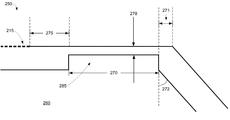
도 2a는 도 1의 예시적인 장치의 일부의 클로즈-업 도시의 개략적인 예시를 제공한다.
도 2b는 도 2a의 일부의 클로즈-업 도시의 개략적인 예시를 제공한다.
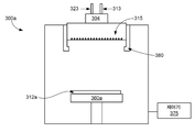
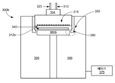
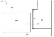
도 3a는 하강된 위치의 페데스탈을 갖는 예시적인 장치의 개략적인 예시를 제공한다.
도 3b는 상승된 위치의 페데스탈을 갖는 예시적인 장치의 개략적인 예시를 제공한다.
도 3c는 도 3b의 부분의 클로즈-업 도시의 개략적인 예시를 제공한다.
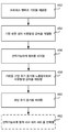
도 4a는 개시된 실시예들에 따라 수행될 수도 있는 방법을 수행하기 위한 동작들의 프로세스 흐름도이다.
도 4b는 개시된 실시예들에 따른 장치에서 수행될 수도 있는 방법을 수행하기 위한 동작들의 프로세스 흐름도이다.
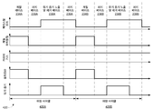
도 4c는 개시된 실시예들에 따른 장치에서 수행될 수도 있는 방법의 사이클들의 예를 도시하는 타이밍 시퀀스도이다.
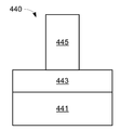
도 4d 내지 도 4g는 개시된 실시예들에 따른 장치에서 수행될 수도 있는 방법을 겪을 수도 있는 예시적인 기판들의 개략적인 예시이다.
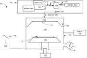
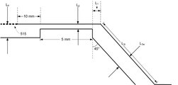
도 5는 실험들에 사용된 프로세스 챔버의 영역의 개략적인 예시이다.
| L 2 (mm) | L 3w (mm) | P avg (mT) | ΔP (mT) | U MM ( %) |
| 0.50 | 0.35 | 2500 | 71 | 1.4 |
| 0.75 | 0.53 | 1440 | 126 | 4.4 |
| 0.90 | 0.64 | 1150 | 160 | 7.0 |
| L 3w (mm) | L 1 (mm) | P avg (mT) | ΔP (mT) | U MM ( %) |
| 1.12 | 1.0 | 840 | 237 | 14.1 |
| 1.32 | 1.5 | 176 | 269 | 17.6 |
| 1.50 | 2.0 | 735 | 284 | 19.3 |
| L 3l (mm) | P avg (mT) | ΔP (mT) | U MM ( %) |
| 70 | 267 | 96 | 18 |
| 128 | 288 | 87 | 15.2 |
| 페데스탈 높이 (mm) | L 3l (mm) | P avg (mT) | ΔP (mT) | U MM ( %) |
| 51 | 156 | 300 | 40 | 6.6 |
| 100 | 205 | 326 | 36 | 5.6 |
| Flow (sccm) | P avg (mT) | ΔP (mT) | U MM ( %) |
| 100 | 326 | 36 | 5.6 |
| 1000 | 986 | 121 | 6.1 |
| 2000 | 1392 | 172 | 6.2 |
| Pump Pressure (mT) | P avg (mT) | ΔP (mT) | U MM ( %) |
| 100 | 1392 | 172 | 6.2 |
| 200 | 1402 | 171 | 6.1 |
| 300 | 1420 | 169 | 5.9 |
| 400 | 1444 | 165 | 5.7 |
| 500 | 1475 | 162 | 5.5 |
Claims (20)
- 반도체 기판을 프로세싱하기 위한 장치에 있어서,
상기 장치는,
프로세스 챔버로서,
상기 장치로 프로세스 가스들을 분배하기 위한 샤워헤드,
상기 반도체 기판을 홀딩하기 위한 이동식 페데스탈로서, 상승된 위치의 상기 이동식 페데스탈이 상기 이동식 페데스탈과 상기 샤워헤드 사이에 상부 챔버 영역 및 상기 이동식 페데스탈 밑에 하부 챔버 영역을 형성하도록 상기 이동식 페데스탈은 상기 상승된 위치 또는 하강된 위치에 위치될 수 있는, 상기 이동식 페데스탈, 및
상기 이동식 페데스탈이 상기 상승된 위치로 이동될 때 상기 이동식 페데스탈의 에지와 정렬할 수 있는 상기 샤워헤드 근방의 영역을 포함하는, 상기 프로세스 챔버;
상기 샤워헤드를 향해 프로세스 가스들을 전달하기 위해 상기 샤워헤드에 커플링된 유입부들;
상기 프로세스 챔버 내에서 플라즈마를 점화하기 위한 플라즈마 생성기; 및
상기 장치의 동작들을 제어하기 위한 제어기로서, 상기 제어기는 상기 상승된 위치 또는 하강된 위치로 상기 페데스탈을 이동시키기 위한 머신-판독가능한 인스트럭션들을 포함하는, 상기 제어기를 포함하고,
상기 이동식 페데스탈이 상기 상승된 위치에 있을 때 상기 상부 챔버 영역과 상기 하부 챔버 영역 사이에 압력 차가 형성되는, 반도체 기판을 프로세싱하기 위한 장치. - 제 1 항에 있어서,
상기 이동식 페데스탈이 상기 상승된 위치에 있을 때 상기 이동식 페데스탈의 에지와 상기 샤워헤드 근방의 상기 영역 사이의 거리는 약 0.3 ㎜ 내지 약 3 ㎜인, 반도체 기판을 프로세싱하기 위한 장치. - 제 1 항에 있어서,
상기 샤워헤드 근방의 상기 영역은 상기 샤워헤드에 수직인 축으로부터 약 45 °로 기울어지는, 반도체 기판을 프로세싱하기 위한 장치. - 제 1 항에 있어서,
상기 샤워헤드 근방의 상기 영역은 상기 장치의 측벽의 일부인, 반도체 기판을 프로세싱하기 위한 장치. - 제 1 항에 있어서,
상기 이동식 페데스탈이 상기 상승된 위치에 있을 때 상기 상부 챔버 영역에서, 상기 샤워헤드와 상기 이동식 페데스탈 사이의 거리는 약 1 ㎜ 내지 약 2 ㎜인, 반도체 기판을 프로세싱하기 위한 장치. - 제 1 항에 있어서,
상기 이동식 페데스탈은 상기 이동식 페데스탈의 상기 에지에 인접한 상승된 영역을 포함하는, 반도체 기판을 프로세싱하기 위한 장치. - 제 1 항에 있어서,
상기 이동식 페데스탈의 상기 에지는 기울어지는, 반도체 기판을 프로세싱하기 위한 장치. - 제 1 항에 있어서,
상기 이동식 페데스탈의 상기 에지는 상기 이동식 페데스탈의 상기 표면에 수직인, 반도체 기판을 프로세싱하기 위한 장치. - 제 1 항 내지 제 8 항 중 어느 한 항에 있어서,
상기 이동식 페데스탈이 상기 상승된 위치에 있을 때 상기 상부 챔버 영역과 상기 하부 챔버 영역 사이의 상기 압력 차는 약 50 mTorr 내지 약 5 Torr인, 반도체 기판을 프로세싱하기 위한 장치. - 제 1 항 내지 제 8 항 중 어느 한 항에 있어서,
상기 이동식 페데스탈이 상기 상승된 위치에 있을 때 상기 상부 챔버 영역의 상기 압력은 상기 이동식 페데스탈이 상기 하강된 위치에 있을 때 상기 상부 챔버의 상기 압력보다 적어도 약 2 내지 약 10,000 배 클 수 있는, 반도체 기판을 프로세싱하기 위한 장치. - 제 1 항 내지 제 8 항 중 어느 한 항에 있어서,
상기 이동식 페데스탈은 상기 하강된 위치와 상기 상승된 위치 사이에서 약 4 인치 내지 약 6 인치의 거리를 이동할 수 있는, 반도체 기판을 프로세싱하기 위한 장치. - 제 1 항 내지 제 8 항 중 어느 한 항에 있어서,
상기 유입부들은 약 1000 sccm보다 큰 플로우 레이트로 상기 프로세스 챔버로 유기 증기를 전달하기 위한 유입부를 포함하는, 반도체 기판을 프로세싱하기 위한 장치. - 제 1 항 내지 제 8 항 중 어느 한 항에 있어서,
상기 유입부들은 플라즈마를 생성하도록 상기 샤워헤드로 염소-함유 프로세스 가스 또는 산소-함유 프로세스 가스를 전달하기 위한 유입부를 포함하는, 반도체 기판을 프로세싱하기 위한 장치. - 제 1 항 내지 제 8 항 중 어느 한 항에 있어서,
상기 이동식 페데스탈의 상기 두께는 약 50 ㎜ 내지 약 100 ㎜인, 반도체 기판을 프로세싱하기 위한 장치. - 제 1 항 내지 제 8 항 중 어느 한 항에 있어서,
상기 제어기는,
상기 기판 상에 개질된 비휘발성 금속을 형성하도록 상기 이동식 페데스탈이 상기 하강된 위치에 있을 때 상기 기판 상의 비휘발성 금속에 상기 플라즈마를 도입하기 위한 머신-판독가능 인스트럭션; 및
상기 개질된 비휘발성 금속을 에칭하도록 상기 이동식 페데스탈이 상기 상승된 위치에 있는 동안 상기 챔버로 유기 증기를 도입하기 위한 머신-판독가능 인스트럭션을 더 포함하는, 반도체 기판을 프로세싱하기 위한 장치. - 제 6 항에 있어서,
상기 샤워헤드에 대해 평면형인 표면과 상기 상승된 영역의 상기 상부 표면 사이의 상기 거리는 약 0 ㎜ 내지 약 1 ㎜인, 반도체 기판을 프로세싱하기 위한 장치. - 제 6 항에 있어서,
상기 상승된 영역은 내측 코너 및 외측 코너를 포함하고, 그리고
상기 샤워헤드의 에지와 상기 내측 코너 사이의 측방향 거리는 약 10 ㎜인, 반도체 기판을 프로세싱하기 위한 장치. - 제 3 항에 있어서,
상기 샤워헤드 근방의 상기 기울어진 영역의 길이는 약 50 ㎜ 내지 약 200 ㎜인, 반도체 기판을 프로세싱하기 위한 장치. - 상승된 위치의 이동식 페데스탈이 상기 이동식 페데스탈과 샤워헤드 사이에 상부 챔버 영역 및 상기 이동식 페데스탈 밑에 하부 챔버 영역을 형성하도록 상기 이동식 페데스탈은 상기 상승된 위치 또는 하강된 위치에 위치될 수 있는, 기판을 홀딩하기 위한 상기 이동식 페데스탈을 포함하는, 프로세스 챔버 내에서 기판 상의 비휘발성 금속을 에칭하는 방법에 있어서,
상기 방법은,
상기 비휘발성 금속을 개질하도록 상기 이동식 페데스탈이 상기 하강된 위치에 있을 때 상기 기판 상의 상기 비휘발성 금속을 플라즈마에 노출시키는 단계; 및
상기 개질된 비휘발성 금속을 제거하도록 상기 이동식 페데스탈이 상기 상승된 위치에 있을 때 상기 개질된 비휘발성 금속을 유기 증기에 노출시키는 단계를 포함하고,
상기 이동식 페데스탈이 상기 상승된 위치에 있을 때 상기 프로세스 챔버 내에서 상기 상부 챔버 영역과 상기 하부 챔버 영역 사이에 압력 차가 형성되는, 프로세스 챔버 내에서 기판 상의 비휘발성 금속을 에칭하는 방법. - 제 19 항에 있어서,
상기 이동식 페데스탈이 상기 상승된 위치에 있을 때 상기 상부 챔버 영역의 상기 압력은 상기 이동식 페데스탈이 상기 하강된 위치에 있을 때 상기 상부 챔버의 압력보다 적어도 약 2 내지 약 10,000 배 큰, 프로세스 챔버 내에서 기판 상의 비휘발성 금속을 에칭하는 방법.
Applications Claiming Priority (2)
| Application Number | Priority Date | Filing Date | Title |
|---|---|---|---|
| US15/017,444 US9953843B2 (en) | 2016-02-05 | 2016-02-05 | Chamber for patterning non-volatile metals |
| US15/017,444 | 2016-02-05 |
Publications (2)
| Publication Number | Publication Date |
|---|---|
| KR20170093716A true KR20170093716A (ko) | 2017-08-16 |
| KR102918166B1 KR102918166B1 (ko) | 2026-01-26 |
Family
ID=59497965
Family Applications (1)
| Application Number | Title | Priority Date | Filing Date |
|---|---|---|---|
| KR1020170013960A Active KR102918166B1 (ko) | 2016-02-05 | 2017-01-31 | 비휘발성 금속들을 패터닝하기 위한 챔버 |
Country Status (5)
| Country | Link |
|---|---|
| US (2) | US9953843B2 (ko) |
| JP (1) | JP6948797B2 (ko) |
| KR (1) | KR102918166B1 (ko) |
| CN (2) | CN107045969B (ko) |
| TW (1) | TWI742034B (ko) |
Families Citing this family (31)
| Publication number | Priority date | Publication date | Assignee | Title |
|---|---|---|---|---|
| CN107548515B (zh) * | 2015-04-24 | 2019-10-15 | 应用材料公司 | 包含流动隔离环的处理套组 |
| US10358721B2 (en) * | 2015-10-22 | 2019-07-23 | Asm Ip Holding B.V. | Semiconductor manufacturing system including deposition apparatus |
| US11251019B2 (en) * | 2016-12-15 | 2022-02-15 | Toyota Jidosha Kabushiki Kaisha | Plasma device |
| JP6863199B2 (ja) | 2017-09-25 | 2021-04-21 | トヨタ自動車株式会社 | プラズマ処理装置 |
| US12012652B2 (en) | 2018-05-21 | 2024-06-18 | Applied Materials, Inc. | Single process volume to perform high-pressure and low-pressure processes with features to reduce cross-contamination |
| JP2022090148A (ja) * | 2019-04-02 | 2022-06-17 | 株式会社Adeka | 原子層エッチング法用エッチング材料 |
| US10998209B2 (en) | 2019-05-31 | 2021-05-04 | Applied Materials, Inc. | Substrate processing platforms including multiple processing chambers |
| TWI910974B (zh) | 2019-06-26 | 2026-01-01 | 美商蘭姆研究公司 | 利用鹵化物化學品的光阻顯影 |
| US11139168B2 (en) * | 2019-12-02 | 2021-10-05 | Applied Materials, Inc. | Chamber deposition and etch process |
| US11424123B2 (en) * | 2020-02-25 | 2022-08-23 | Tokyo Electron Limited | Forming a semiconductor feature using atomic layer etch |
| US12080571B2 (en) | 2020-07-08 | 2024-09-03 | Applied Materials, Inc. | Substrate processing module and method of moving a workpiece |
| JP7174016B2 (ja) * | 2020-07-16 | 2022-11-17 | 株式会社Kokusai Electric | 基板処理方法、半導体装置の製造方法、基板処理装置、およびプログラム |
| US11749542B2 (en) | 2020-07-27 | 2023-09-05 | Applied Materials, Inc. | Apparatus, system, and method for non-contact temperature monitoring of substrate supports |
| US11817331B2 (en) | 2020-07-27 | 2023-11-14 | Applied Materials, Inc. | Substrate holder replacement with protective disk during pasting process |
| US11501957B2 (en) * | 2020-09-03 | 2022-11-15 | Applied Materials, Inc. | Pedestal support design for precise chamber matching and process control |
| US11600507B2 (en) | 2020-09-09 | 2023-03-07 | Applied Materials, Inc. | Pedestal assembly for a substrate processing chamber |
| US11610799B2 (en) | 2020-09-18 | 2023-03-21 | Applied Materials, Inc. | Electrostatic chuck having a heating and chucking capabilities |
| WO2022103764A1 (en) | 2020-11-13 | 2022-05-19 | Lam Research Corporation | Process tool for dry removal of photoresist |
| US12577466B2 (en) | 2020-12-08 | 2026-03-17 | Lam Research Corporation | Photoresist development with organic vapor |
| US20240021435A1 (en) * | 2021-01-15 | 2024-01-18 | Lam Research Corporation | Metal etch |
| US12195314B2 (en) | 2021-02-02 | 2025-01-14 | Applied Materials, Inc. | Cathode exchange mechanism to improve preventative maintenance time for cluster system |
| US11674227B2 (en) | 2021-02-03 | 2023-06-13 | Applied Materials, Inc. | Symmetric pump down mini-volume with laminar flow cavity gas injection for high and low pressure |
| JP7591962B2 (ja) * | 2021-03-30 | 2024-11-29 | 株式会社アルバック | 真空処理方法及び真空処理装置 |
| US12002668B2 (en) | 2021-06-25 | 2024-06-04 | Applied Materials, Inc. | Thermal management hardware for uniform temperature control for enhanced bake-out for cluster tool |
| US20230113063A1 (en) * | 2021-10-11 | 2023-04-13 | Applied Materials, Inc. | Dynamic processing chamber baffle |
| KR102765372B1 (ko) * | 2021-11-16 | 2025-02-11 | 세메스 주식회사 | 기판 처리 장치 및 방법 |
| KR20230085072A (ko) * | 2021-12-06 | 2023-06-13 | 에이에스엠 아이피 홀딩 비.브이. | 반도체 처리 툴용 반응물 증기 전달 시스템 및 방법 |
| KR102725782B1 (ko) | 2022-07-01 | 2024-11-05 | 램 리써치 코포레이션 | 에칭 정지 억제 (etch stop deterrence) 를 위한 금속 옥사이드 기반 포토레지스트의 순환적 현상 |
| WO2024196643A1 (en) | 2023-03-17 | 2024-09-26 | Lam Research Corporation | Integration of dry development and etch processes for euv patterning in a single process chamber |
| CN121153106A (zh) * | 2023-04-14 | 2025-12-16 | 弗萨姆材料美国有限责任公司 | 含金属材料的气相蚀刻 |
| KR20250034920A (ko) | 2023-07-27 | 2025-03-11 | 램 리써치 코포레이션 | 금속-함유 포토레지스트에 대한 올-인-원 건식 현상 |
Citations (3)
| Publication number | Priority date | Publication date | Assignee | Title |
|---|---|---|---|---|
| JP2002343787A (ja) * | 2001-05-17 | 2002-11-29 | Research Institute Of Innovative Technology For The Earth | プラズマ処理装置およびそのクリーニング方法 |
| JP2004200345A (ja) * | 2002-12-18 | 2004-07-15 | Hitachi Kokusai Electric Inc | プラズマ処理装置 |
| KR20070055874A (ko) * | 2005-11-28 | 2007-05-31 | 삼성전자주식회사 | 플라즈마 처리 장치 |
Family Cites Families (38)
| Publication number | Priority date | Publication date | Assignee | Title |
|---|---|---|---|---|
| US5429070A (en) | 1989-06-13 | 1995-07-04 | Plasma & Materials Technologies, Inc. | High density plasma deposition and etching apparatus |
| JPH0613361A (ja) | 1992-06-26 | 1994-01-21 | Tokyo Electron Ltd | 処理装置 |
| JP3210207B2 (ja) * | 1994-04-20 | 2001-09-17 | 東京エレクトロン株式会社 | プラズマ処理装置 |
| US6296711B1 (en) * | 1998-04-14 | 2001-10-02 | Cvd Systems, Inc. | Film processing system |
| KR100292410B1 (ko) * | 1998-09-23 | 2001-06-01 | 윤종용 | 불순물 오염이 억제된 반도체 제조용 반응 챔버 |
| US20030101938A1 (en) * | 1998-10-27 | 2003-06-05 | Applied Materials, Inc. | Apparatus for the deposition of high dielectric constant films |
| US6409837B1 (en) | 1999-01-13 | 2002-06-25 | Tokyo Electron Limited | Processing system and method for chemical vapor deposition of a metal layer using a liquid precursor |
| US6419751B1 (en) | 1999-07-26 | 2002-07-16 | Tokyo Electron Limited | Substrate processing method and substrate processing apparatus |
| KR100338768B1 (ko) * | 1999-10-25 | 2002-05-30 | 윤종용 | 산화막 제거방법 및 산화막 제거를 위한 반도체 제조 장치 |
| US7085616B2 (en) | 2001-07-27 | 2006-08-01 | Applied Materials, Inc. | Atomic layer deposition apparatus |
| WO2003038145A2 (en) | 2001-10-29 | 2003-05-08 | Genus, Inc. | Chemical vapor deposition system |
| US20030211244A1 (en) * | 2002-04-11 | 2003-11-13 | Applied Materials, Inc. | Reacting an organosilicon compound with an oxidizing gas to form an ultra low k dielectric |
| US7160577B2 (en) | 2002-05-02 | 2007-01-09 | Micron Technology, Inc. | Methods for atomic-layer deposition of aluminum oxides in integrated circuits |
| US6936551B2 (en) * | 2002-05-08 | 2005-08-30 | Applied Materials Inc. | Methods and apparatus for E-beam treatment used to fabricate integrated circuit devices |
| JP4338355B2 (ja) * | 2002-05-10 | 2009-10-07 | 東京エレクトロン株式会社 | プラズマ処理装置 |
| US6846380B2 (en) | 2002-06-13 | 2005-01-25 | The Boc Group, Inc. | Substrate processing apparatus and related systems and methods |
| US6821347B2 (en) | 2002-07-08 | 2004-11-23 | Micron Technology, Inc. | Apparatus and method for depositing materials onto microelectronic workpieces |
| JP2004119448A (ja) * | 2002-09-24 | 2004-04-15 | Nec Kyushu Ltd | プラズマエッチング装置およびプラズマエッチング方法 |
| US7031600B2 (en) * | 2003-04-07 | 2006-04-18 | Applied Materials, Inc. | Method and apparatus for silicon oxide deposition on large area substrates |
| US7700155B1 (en) | 2004-04-08 | 2010-04-20 | Novellus Systems, Inc. | Method and apparatus for modulation of precursor exposure during a pulsed deposition process |
| US7699932B2 (en) | 2004-06-02 | 2010-04-20 | Micron Technology, Inc. | Reactors, systems and methods for depositing thin films onto microfeature workpieces |
| KR100790392B1 (ko) | 2004-11-12 | 2008-01-02 | 삼성전자주식회사 | 반도체 제조장치 |
| US7422983B2 (en) | 2005-02-24 | 2008-09-09 | International Business Machines Corporation | Ta-TaN selective removal process for integrated device fabrication |
| US20070068623A1 (en) * | 2005-09-27 | 2007-03-29 | Yunsang Kim | Apparatus for the removal of a set of byproducts from a substrate edge and methods therefor |
| US7909960B2 (en) * | 2005-09-27 | 2011-03-22 | Lam Research Corporation | Apparatus and methods to remove films on bevel edge and backside of wafer |
| US20080178805A1 (en) * | 2006-12-05 | 2008-07-31 | Applied Materials, Inc. | Mid-chamber gas distribution plate, tuned plasma flow control grid and electrode |
| US8580078B2 (en) * | 2007-01-26 | 2013-11-12 | Lam Research Corporation | Bevel etcher with vacuum chuck |
| CN101802986B (zh) * | 2007-07-11 | 2012-09-26 | 东京毅力科创株式会社 | 等离子体处理方法和等离子体处理装置 |
| JP2011503899A (ja) | 2007-11-16 | 2011-01-27 | イー.ケー.シー.テクノロジー.インコーポレーテッド | 半導体基板から金属ハードマスクエッチング残留物を除去するための組成物 |
| US20090178763A1 (en) * | 2008-01-10 | 2009-07-16 | Applied Materials, Inc. | Showerhead insulator and etch chamber liner |
| US8129288B2 (en) * | 2008-05-02 | 2012-03-06 | Intermolecular, Inc. | Combinatorial plasma enhanced deposition techniques |
| JP5497278B2 (ja) * | 2008-07-17 | 2014-05-21 | 東京エレクトロン株式会社 | 銅の異方性ドライエッチング方法および装置 |
| US8869741B2 (en) * | 2008-12-19 | 2014-10-28 | Lam Research Corporation | Methods and apparatus for dual confinement and ultra-high pressure in an adjustable gap plasma chamber |
| KR101711687B1 (ko) * | 2009-09-28 | 2017-03-02 | 램 리써치 코포레이션 | 일체형 한정 링 배열 및 그 방법 |
| JP5675138B2 (ja) * | 2010-03-25 | 2015-02-25 | 東京エレクトロン株式会社 | プラズマ処理装置 |
| WO2014092856A1 (en) | 2012-12-14 | 2014-06-19 | The Penn State Research Foundation | Ultra-high speed anisotropic reactive ion etching |
| US10351956B2 (en) * | 2013-03-14 | 2019-07-16 | Applied Materials, Inc. | Integrated two-axis lift-rotation motor center pedestal in multi-wafer carousel ALD |
| US9257638B2 (en) * | 2014-03-27 | 2016-02-09 | Lam Research Corporation | Method to etch non-volatile metal materials |
-
2016
- 2016-02-05 US US15/017,444 patent/US9953843B2/en active Active
-
2017
- 2017-01-25 TW TW106102778A patent/TWI742034B/zh active
- 2017-01-26 CN CN201710061612.5A patent/CN107045969B/zh active Active
- 2017-01-26 CN CN201910092850.1A patent/CN110112048A/zh active Pending
- 2017-01-31 KR KR1020170013960A patent/KR102918166B1/ko active Active
- 2017-02-01 JP JP2017016396A patent/JP6948797B2/ja active Active
-
2018
- 2018-03-15 US US15/922,705 patent/US20180204738A1/en not_active Abandoned
Patent Citations (3)
| Publication number | Priority date | Publication date | Assignee | Title |
|---|---|---|---|---|
| JP2002343787A (ja) * | 2001-05-17 | 2002-11-29 | Research Institute Of Innovative Technology For The Earth | プラズマ処理装置およびそのクリーニング方法 |
| JP2004200345A (ja) * | 2002-12-18 | 2004-07-15 | Hitachi Kokusai Electric Inc | プラズマ処理装置 |
| KR20070055874A (ko) * | 2005-11-28 | 2007-05-31 | 삼성전자주식회사 | 플라즈마 처리 장치 |
Also Published As
| Publication number | Publication date |
|---|---|
| TW201740465A (zh) | 2017-11-16 |
| CN110112048A (zh) | 2019-08-09 |
| CN107045969A (zh) | 2017-08-15 |
| KR102918166B1 (ko) | 2026-01-26 |
| US9953843B2 (en) | 2018-04-24 |
| US20170229317A1 (en) | 2017-08-10 |
| TWI742034B (zh) | 2021-10-11 |
| CN107045969B (zh) | 2020-05-22 |
| JP2017152689A (ja) | 2017-08-31 |
| JP6948797B2 (ja) | 2021-10-13 |
| US20180204738A1 (en) | 2018-07-19 |
Similar Documents
| Publication | Publication Date | Title |
|---|---|---|
| KR102918166B1 (ko) | 비휘발성 금속들을 패터닝하기 위한 챔버 | |
| KR102821470B1 (ko) | 알루미늄 옥사이드 에칭 정지층들의 증착 | |
| US11479856B2 (en) | Multi-cycle ALD process for film uniformity and thickness profile modulation | |
| US10832909B2 (en) | Atomic layer etch, reactive precursors and energetic sources for patterning applications | |
| KR102695879B1 (ko) | 포토레지스트 패터닝 스컴 (scum) 의 제거를 위한 원자 층 세정 | |
| US9997371B1 (en) | Atomic layer etch methods and hardware for patterning applications | |
| KR101701024B1 (ko) | 컨포멀한 알루미늄 질화물을 위한 고 성장 레이트 프로세스 | |
| US12606905B2 (en) | Chamfer-less via integration scheme | |
| KR102933663B1 (ko) | 고 종횡비 구조체들의 효율적인 세정 및 에칭 | |
| KR20170044014A (ko) | 로우-k 알루미늄 함유 에칭 정지막들의 형성을 위한 방법들 | |
| US10651080B2 (en) | Oxidizing treatment of aluminum nitride films in semiconductor device manufacturing | |
| JP2023516588A (ja) | Euvパターニングにおける欠陥低減のための多層ハードマスク |
Legal Events
| Date | Code | Title | Description |
|---|---|---|---|
| E13-X000 | Pre-grant limitation requested |
St.27 status event code: A-2-3-E10-E13-lim-X000 |
|
| PA0109 | Patent application |
St.27 status event code: A-0-1-A10-A12-nap-PA0109 |
|
| P11-X000 | Amendment of application requested |
St.27 status event code: A-2-2-P10-P11-nap-X000 |
|
| P13-X000 | Application amended |
St.27 status event code: A-2-2-P10-P13-nap-X000 |
|
| PG1501 | Laying open of application |
St.27 status event code: A-1-1-Q10-Q12-nap-PG1501 |
|
| A201 | Request for examination | ||
| P11-X000 | Amendment of application requested |
St.27 status event code: A-2-2-P10-P11-nap-X000 |
|
| P13-X000 | Application amended |
St.27 status event code: A-2-2-P10-P13-nap-X000 |
|
| PA0201 | Request for examination |
St.27 status event code: A-1-2-D10-D11-exm-PA0201 |
|
| E902 | Notification of reason for refusal | ||
| PE0902 | Notice of grounds for rejection |
St.27 status event code: A-1-2-D10-D21-exm-PE0902 |
|
| T11-X000 | Administrative time limit extension requested |
St.27 status event code: U-3-3-T10-T11-oth-X000 |
|
| P11-X000 | Amendment of application requested |
St.27 status event code: A-2-2-P10-P11-nap-X000 |
|
| P13-X000 | Application amended |
St.27 status event code: A-2-2-P10-P13-nap-X000 |
|
| E601 | Decision to refuse application | ||
| PE0601 | Decision on rejection of patent |
St.27 status event code: N-2-6-B10-B15-exm-PE0601 |
|
| E13-X000 | Pre-grant limitation requested |
St.27 status event code: A-2-3-E10-E13-lim-X000 |
|
| P11-X000 | Amendment of application requested |
St.27 status event code: A-2-2-P10-P11-nap-X000 |
|
| F13 | Ip right granted in full following pre-grant review |
Free format text: ST27 STATUS EVENT CODE: A-3-4-F10-F13-REX-PX0701 (AS PROVIDED BY THE NATIONAL OFFICE) |
|
| PX0701 | Decision of registration after re-examination |
St.27 status event code: A-3-4-F10-F13-rex-PX0701 |
|
| P22-X000 | Classification modified |
St.27 status event code: A-2-2-P10-P22-nap-X000 |
|
| F11 | Ip right granted following substantive examination |
Free format text: ST27 STATUS EVENT CODE: A-2-4-F10-F11-EXM-PR0701 (AS PROVIDED BY THE NATIONAL OFFICE) |
|
| PR0701 | Registration of establishment |
St.27 status event code: A-2-4-F10-F11-exm-PR0701 |
|
| PR1002 | Payment of registration fee |
St.27 status event code: A-2-2-U10-U11-oth-PR1002 Fee payment year number: 1 |
|
| U11 | Full renewal or maintenance fee paid |
Free format text: ST27 STATUS EVENT CODE: A-2-2-U10-U11-OTH-PR1002 (AS PROVIDED BY THE NATIONAL OFFICE) Year of fee payment: 1 |
|
| PG1601 | Publication of registration |
St.27 status event code: A-4-4-Q10-Q13-nap-PG1601 |
|
| Q13 | Ip right document published |
Free format text: ST27 STATUS EVENT CODE: A-4-4-Q10-Q13-NAP-PG1601 (AS PROVIDED BY THE NATIONAL OFFICE) |