KR20170096155A - 이동 가능한 스퍼터 조립체 및 전력 파라미터들에 대한 제어를 이용하여 기판을 코팅하기 위한 장치 및 방법 - Google Patents
이동 가능한 스퍼터 조립체 및 전력 파라미터들에 대한 제어를 이용하여 기판을 코팅하기 위한 장치 및 방법 Download PDFInfo
- Publication number
- KR20170096155A KR20170096155A KR1020177019752A KR20177019752A KR20170096155A KR 20170096155 A KR20170096155 A KR 20170096155A KR 1020177019752 A KR1020177019752 A KR 1020177019752A KR 20177019752 A KR20177019752 A KR 20177019752A KR 20170096155 A KR20170096155 A KR 20170096155A
- Authority
- KR
- South Korea
- Prior art keywords
- sputter
- substrate
- source
- power
- sputter source
- Prior art date
- Legal status (The legal status is an assumption and is not a legal conclusion. Google has not performed a legal analysis and makes no representation as to the accuracy of the status listed.)
- Ceased
Links
- 238000000034 method Methods 0.000 title claims abstract description 327
- 239000000758 substrate Substances 0.000 title claims abstract description 176
- 238000000576 coating method Methods 0.000 title claims abstract description 52
- 239000011248 coating agent Substances 0.000 title claims abstract description 51
- 230000008569 process Effects 0.000 claims abstract description 273
- 238000004544 sputter deposition Methods 0.000 claims abstract description 43
- 230000033001 locomotion Effects 0.000 claims abstract description 38
- 239000000463 material Substances 0.000 claims abstract description 36
- 238000009826 distribution Methods 0.000 claims description 45
- 238000013519 translation Methods 0.000 claims description 5
- 230000000694 effects Effects 0.000 claims description 4
- 239000007789 gas Substances 0.000 description 271
- 238000012545 processing Methods 0.000 description 24
- 239000000203 mixture Substances 0.000 description 23
- 230000001276 controlling effect Effects 0.000 description 14
- 238000005546 reactive sputtering Methods 0.000 description 10
- 238000005086 pumping Methods 0.000 description 8
- 230000007704 transition Effects 0.000 description 6
- 238000004519 manufacturing process Methods 0.000 description 5
- IJGRMHOSHXDMSA-UHFFFAOYSA-N Atomic nitrogen Chemical compound N#N IJGRMHOSHXDMSA-UHFFFAOYSA-N 0.000 description 4
- 238000000151 deposition Methods 0.000 description 4
- 230000008021 deposition Effects 0.000 description 4
- 239000013077 target material Substances 0.000 description 3
- XKRFYHLGVUSROY-UHFFFAOYSA-N Argon Chemical compound [Ar] XKRFYHLGVUSROY-UHFFFAOYSA-N 0.000 description 2
- 229910052786 argon Inorganic materials 0.000 description 2
- 125000004429 atom Chemical group 0.000 description 2
- QVGXLLKOCUKJST-UHFFFAOYSA-N atomic oxygen Chemical compound [O] QVGXLLKOCUKJST-UHFFFAOYSA-N 0.000 description 2
- 230000008859 change Effects 0.000 description 2
- 238000005137 deposition process Methods 0.000 description 2
- 230000006870 function Effects 0.000 description 2
- 239000011521 glass Substances 0.000 description 2
- 229910052743 krypton Inorganic materials 0.000 description 2
- 239000002184 metal Substances 0.000 description 2
- 229910052751 metal Inorganic materials 0.000 description 2
- 238000001465 metallisation Methods 0.000 description 2
- 229910052754 neon Inorganic materials 0.000 description 2
- 229910052757 nitrogen Inorganic materials 0.000 description 2
- 230000003287 optical effect Effects 0.000 description 2
- 239000001301 oxygen Substances 0.000 description 2
- 229910052760 oxygen Inorganic materials 0.000 description 2
- 238000004806 packaging method and process Methods 0.000 description 2
- 229910052698 phosphorus Inorganic materials 0.000 description 2
- 239000004065 semiconductor Substances 0.000 description 2
- 229910052710 silicon Inorganic materials 0.000 description 2
- 238000003860 storage Methods 0.000 description 2
- 238000012546 transfer Methods 0.000 description 2
- 235000012431 wafers Nutrition 0.000 description 2
- XLYOFNOQVPJJNP-UHFFFAOYSA-N water Chemical compound O XLYOFNOQVPJJNP-UHFFFAOYSA-N 0.000 description 2
- 229910052724 xenon Inorganic materials 0.000 description 2
- XUIMIQQOPSSXEZ-UHFFFAOYSA-N Silicon Chemical compound [Si] XUIMIQQOPSSXEZ-UHFFFAOYSA-N 0.000 description 1
- 239000000956 alloy Substances 0.000 description 1
- 229910045601 alloy Inorganic materials 0.000 description 1
- 229910052782 aluminium Inorganic materials 0.000 description 1
- 238000005452 bending Methods 0.000 description 1
- 230000015572 biosynthetic process Effects 0.000 description 1
- 238000006243 chemical reaction Methods 0.000 description 1
- 229910052802 copper Inorganic materials 0.000 description 1
- 238000005260 corrosion Methods 0.000 description 1
- 230000007797 corrosion Effects 0.000 description 1
- 239000013078 crystal Substances 0.000 description 1
- 230000001419 dependent effect Effects 0.000 description 1
- 238000010586 diagram Methods 0.000 description 1
- 239000003989 dielectric material Substances 0.000 description 1
- 239000012530 fluid Substances 0.000 description 1
- 239000011888 foil Substances 0.000 description 1
- 239000000446 fuel Substances 0.000 description 1
- 239000001257 hydrogen Substances 0.000 description 1
- 229910052739 hydrogen Inorganic materials 0.000 description 1
- 125000004435 hydrogen atom Chemical class [H]* 0.000 description 1
- 229910052738 indium Inorganic materials 0.000 description 1
- 239000011261 inert gas Substances 0.000 description 1
- 150000002500 ions Chemical class 0.000 description 1
- 230000001788 irregular Effects 0.000 description 1
- DNNSSWSSYDEUBZ-UHFFFAOYSA-N krypton atom Chemical compound [Kr] DNNSSWSSYDEUBZ-UHFFFAOYSA-N 0.000 description 1
- 238000001755 magnetron sputter deposition Methods 0.000 description 1
- 238000012986 modification Methods 0.000 description 1
- 230000004048 modification Effects 0.000 description 1
- 229910052750 molybdenum Inorganic materials 0.000 description 1
- 238000000465 moulding Methods 0.000 description 1
- GKAOGPIIYCISHV-UHFFFAOYSA-N neon atom Chemical compound [Ne] GKAOGPIIYCISHV-UHFFFAOYSA-N 0.000 description 1
- 229910052758 niobium Inorganic materials 0.000 description 1
- 239000010955 niobium Substances 0.000 description 1
- 230000005693 optoelectronics Effects 0.000 description 1
- 239000002245 particle Substances 0.000 description 1
- 238000000059 patterning Methods 0.000 description 1
- 229920000642 polymer Polymers 0.000 description 1
- 229920000307 polymer substrate Polymers 0.000 description 1
- 230000008092 positive effect Effects 0.000 description 1
- 239000000376 reactant Substances 0.000 description 1
- 230000001105 regulatory effect Effects 0.000 description 1
- 239000010703 silicon Substances 0.000 description 1
- 230000003068 static effect Effects 0.000 description 1
- 239000000126 substance Substances 0.000 description 1
- 239000010409 thin film Substances 0.000 description 1
- 229910052719 titanium Inorganic materials 0.000 description 1
- 229910052721 tungsten Inorganic materials 0.000 description 1
- FHNFHKCVQCLJFQ-UHFFFAOYSA-N xenon atom Chemical compound [Xe] FHNFHKCVQCLJFQ-UHFFFAOYSA-N 0.000 description 1
Images


Classifications
-
- C—CHEMISTRY; METALLURGY
- C23—COATING METALLIC MATERIAL; COATING MATERIAL WITH METALLIC MATERIAL; CHEMICAL SURFACE TREATMENT; DIFFUSION TREATMENT OF METALLIC MATERIAL; COATING BY VACUUM EVAPORATION, BY SPUTTERING, BY ION IMPLANTATION OR BY CHEMICAL VAPOUR DEPOSITION, IN GENERAL; INHIBITING CORROSION OF METALLIC MATERIAL OR INCRUSTATION IN GENERAL
- C23C—COATING METALLIC MATERIAL; COATING MATERIAL WITH METALLIC MATERIAL; SURFACE TREATMENT OF METALLIC MATERIAL BY DIFFUSION INTO THE SURFACE, BY CHEMICAL CONVERSION OR SUBSTITUTION; COATING BY VACUUM EVAPORATION, BY SPUTTERING, BY ION IMPLANTATION OR BY CHEMICAL VAPOUR DEPOSITION, IN GENERAL
- C23C14/00—Coating by vacuum evaporation, by sputtering or by ion implantation of the coating forming material
- C23C14/0021—Reactive sputtering or evaporation
- C23C14/0036—Reactive sputtering
- C23C14/0063—Reactive sputtering characterised by means for introducing or removing gases
-
- C—CHEMISTRY; METALLURGY
- C23—COATING METALLIC MATERIAL; COATING MATERIAL WITH METALLIC MATERIAL; CHEMICAL SURFACE TREATMENT; DIFFUSION TREATMENT OF METALLIC MATERIAL; COATING BY VACUUM EVAPORATION, BY SPUTTERING, BY ION IMPLANTATION OR BY CHEMICAL VAPOUR DEPOSITION, IN GENERAL; INHIBITING CORROSION OF METALLIC MATERIAL OR INCRUSTATION IN GENERAL
- C23C—COATING METALLIC MATERIAL; COATING MATERIAL WITH METALLIC MATERIAL; SURFACE TREATMENT OF METALLIC MATERIAL BY DIFFUSION INTO THE SURFACE, BY CHEMICAL CONVERSION OR SUBSTITUTION; COATING BY VACUUM EVAPORATION, BY SPUTTERING, BY ION IMPLANTATION OR BY CHEMICAL VAPOUR DEPOSITION, IN GENERAL
- C23C14/00—Coating by vacuum evaporation, by sputtering or by ion implantation of the coating forming material
- C23C14/22—Coating by vacuum evaporation, by sputtering or by ion implantation of the coating forming material characterised by the process of coating
- C23C14/34—Sputtering
- C23C14/3492—Variation of parameters during sputtering
-
- C—CHEMISTRY; METALLURGY
- C23—COATING METALLIC MATERIAL; COATING MATERIAL WITH METALLIC MATERIAL; CHEMICAL SURFACE TREATMENT; DIFFUSION TREATMENT OF METALLIC MATERIAL; COATING BY VACUUM EVAPORATION, BY SPUTTERING, BY ION IMPLANTATION OR BY CHEMICAL VAPOUR DEPOSITION, IN GENERAL; INHIBITING CORROSION OF METALLIC MATERIAL OR INCRUSTATION IN GENERAL
- C23C—COATING METALLIC MATERIAL; COATING MATERIAL WITH METALLIC MATERIAL; SURFACE TREATMENT OF METALLIC MATERIAL BY DIFFUSION INTO THE SURFACE, BY CHEMICAL CONVERSION OR SUBSTITUTION; COATING BY VACUUM EVAPORATION, BY SPUTTERING, BY ION IMPLANTATION OR BY CHEMICAL VAPOUR DEPOSITION, IN GENERAL
- C23C14/00—Coating by vacuum evaporation, by sputtering or by ion implantation of the coating forming material
- C23C14/22—Coating by vacuum evaporation, by sputtering or by ion implantation of the coating forming material characterised by the process of coating
- C23C14/34—Sputtering
- C23C14/35—Sputtering by application of a magnetic field, e.g. magnetron sputtering
- C23C14/352—Sputtering by application of a magnetic field, e.g. magnetron sputtering using more than one target
-
- C—CHEMISTRY; METALLURGY
- C23—COATING METALLIC MATERIAL; COATING MATERIAL WITH METALLIC MATERIAL; CHEMICAL SURFACE TREATMENT; DIFFUSION TREATMENT OF METALLIC MATERIAL; COATING BY VACUUM EVAPORATION, BY SPUTTERING, BY ION IMPLANTATION OR BY CHEMICAL VAPOUR DEPOSITION, IN GENERAL; INHIBITING CORROSION OF METALLIC MATERIAL OR INCRUSTATION IN GENERAL
- C23C—COATING METALLIC MATERIAL; COATING MATERIAL WITH METALLIC MATERIAL; SURFACE TREATMENT OF METALLIC MATERIAL BY DIFFUSION INTO THE SURFACE, BY CHEMICAL CONVERSION OR SUBSTITUTION; COATING BY VACUUM EVAPORATION, BY SPUTTERING, BY ION IMPLANTATION OR BY CHEMICAL VAPOUR DEPOSITION, IN GENERAL
- C23C14/00—Coating by vacuum evaporation, by sputtering or by ion implantation of the coating forming material
- C23C14/22—Coating by vacuum evaporation, by sputtering or by ion implantation of the coating forming material characterised by the process of coating
- C23C14/54—Controlling or regulating the coating process
-
- C—CHEMISTRY; METALLURGY
- C23—COATING METALLIC MATERIAL; COATING MATERIAL WITH METALLIC MATERIAL; CHEMICAL SURFACE TREATMENT; DIFFUSION TREATMENT OF METALLIC MATERIAL; COATING BY VACUUM EVAPORATION, BY SPUTTERING, BY ION IMPLANTATION OR BY CHEMICAL VAPOUR DEPOSITION, IN GENERAL; INHIBITING CORROSION OF METALLIC MATERIAL OR INCRUSTATION IN GENERAL
- C23C—COATING METALLIC MATERIAL; COATING MATERIAL WITH METALLIC MATERIAL; SURFACE TREATMENT OF METALLIC MATERIAL BY DIFFUSION INTO THE SURFACE, BY CHEMICAL CONVERSION OR SUBSTITUTION; COATING BY VACUUM EVAPORATION, BY SPUTTERING, BY ION IMPLANTATION OR BY CHEMICAL VAPOUR DEPOSITION, IN GENERAL
- C23C14/00—Coating by vacuum evaporation, by sputtering or by ion implantation of the coating forming material
- C23C14/22—Coating by vacuum evaporation, by sputtering or by ion implantation of the coating forming material characterised by the process of coating
- C23C14/54—Controlling or regulating the coating process
- C23C14/542—Controlling the film thickness or evaporation rate
-
- C—CHEMISTRY; METALLURGY
- C23—COATING METALLIC MATERIAL; COATING MATERIAL WITH METALLIC MATERIAL; CHEMICAL SURFACE TREATMENT; DIFFUSION TREATMENT OF METALLIC MATERIAL; COATING BY VACUUM EVAPORATION, BY SPUTTERING, BY ION IMPLANTATION OR BY CHEMICAL VAPOUR DEPOSITION, IN GENERAL; INHIBITING CORROSION OF METALLIC MATERIAL OR INCRUSTATION IN GENERAL
- C23C—COATING METALLIC MATERIAL; COATING MATERIAL WITH METALLIC MATERIAL; SURFACE TREATMENT OF METALLIC MATERIAL BY DIFFUSION INTO THE SURFACE, BY CHEMICAL CONVERSION OR SUBSTITUTION; COATING BY VACUUM EVAPORATION, BY SPUTTERING, BY ION IMPLANTATION OR BY CHEMICAL VAPOUR DEPOSITION, IN GENERAL
- C23C14/00—Coating by vacuum evaporation, by sputtering or by ion implantation of the coating forming material
- C23C14/22—Coating by vacuum evaporation, by sputtering or by ion implantation of the coating forming material characterised by the process of coating
- C23C14/56—Apparatus specially adapted for continuous coating; Arrangements for maintaining the vacuum, e.g. vacuum locks
- C23C14/562—Apparatus specially adapted for continuous coating; Arrangements for maintaining the vacuum, e.g. vacuum locks for coating elongated substrates
-
- H—ELECTRICITY
- H01—ELECTRIC ELEMENTS
- H01J—ELECTRIC DISCHARGE TUBES OR DISCHARGE LAMPS
- H01J37/00—Discharge tubes with provision for introducing objects or material to be exposed to the discharge, e.g. for the purpose of examination or processing thereof
- H01J37/32—Gas-filled discharge tubes
- H01J37/32431—Constructional details of the reactor
- H01J37/32733—Means for moving the material to be treated
-
- H—ELECTRICITY
- H01—ELECTRIC ELEMENTS
- H01J—ELECTRIC DISCHARGE TUBES OR DISCHARGE LAMPS
- H01J37/00—Discharge tubes with provision for introducing objects or material to be exposed to the discharge, e.g. for the purpose of examination or processing thereof
- H01J37/32—Gas-filled discharge tubes
- H01J37/34—Gas-filled discharge tubes operating with cathodic sputtering
- H01J37/3402—Gas-filled discharge tubes operating with cathodic sputtering using supplementary magnetic fields
- H01J37/3405—Magnetron sputtering
-
- H—ELECTRICITY
- H01—ELECTRIC ELEMENTS
- H01J—ELECTRIC DISCHARGE TUBES OR DISCHARGE LAMPS
- H01J37/00—Discharge tubes with provision for introducing objects or material to be exposed to the discharge, e.g. for the purpose of examination or processing thereof
- H01J37/32—Gas-filled discharge tubes
- H01J37/34—Gas-filled discharge tubes operating with cathodic sputtering
- H01J37/3411—Constructional aspects of the reactor
- H01J37/3414—Targets
- H01J37/3417—Arrangements
-
- H—ELECTRICITY
- H01—ELECTRIC ELEMENTS
- H01J—ELECTRIC DISCHARGE TUBES OR DISCHARGE LAMPS
- H01J37/00—Discharge tubes with provision for introducing objects or material to be exposed to the discharge, e.g. for the purpose of examination or processing thereof
- H01J37/32—Gas-filled discharge tubes
- H01J37/34—Gas-filled discharge tubes operating with cathodic sputtering
- H01J37/3411—Constructional aspects of the reactor
- H01J37/3444—Associated circuits
-
- H—ELECTRICITY
- H01—ELECTRIC ELEMENTS
- H01J—ELECTRIC DISCHARGE TUBES OR DISCHARGE LAMPS
- H01J37/00—Discharge tubes with provision for introducing objects or material to be exposed to the discharge, e.g. for the purpose of examination or processing thereof
- H01J37/32—Gas-filled discharge tubes
- H01J37/34—Gas-filled discharge tubes operating with cathodic sputtering
- H01J37/3411—Constructional aspects of the reactor
- H01J37/3447—Collimators, shutters, apertures
-
- H—ELECTRICITY
- H01—ELECTRIC ELEMENTS
- H01J—ELECTRIC DISCHARGE TUBES OR DISCHARGE LAMPS
- H01J37/00—Discharge tubes with provision for introducing objects or material to be exposed to the discharge, e.g. for the purpose of examination or processing thereof
- H01J37/32—Gas-filled discharge tubes
- H01J37/34—Gas-filled discharge tubes operating with cathodic sputtering
- H01J37/3464—Operating strategies
- H01J37/347—Thickness uniformity of coated layers or desired profile of target erosion
Landscapes
- Chemical & Material Sciences (AREA)
- Engineering & Computer Science (AREA)
- Chemical Kinetics & Catalysis (AREA)
- Materials Engineering (AREA)
- Mechanical Engineering (AREA)
- Metallurgy (AREA)
- Organic Chemistry (AREA)
- Physics & Mathematics (AREA)
- Plasma & Fusion (AREA)
- Analytical Chemistry (AREA)
- Physical Vapour Deposition (AREA)
Abstract
Description
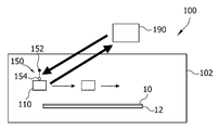
도 1은, 본원에서 설명되는 실시예들에 따른, 기판을 코팅하기 위한 장치의 개략도를 도시하고;
도 2는, 본원에서 설명되는 실시예들에 따른, 기판을 코팅하기 위한 장치의 실시예를 도시하며;
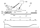
도 3은, 비-제한적인 예로써, 도 2의 실시예의 작동 원리를 예시하고;
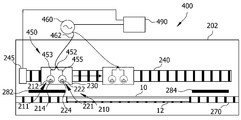
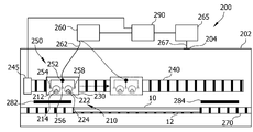
도 4-5는, 기판을 코팅하기 위한 장치의 추가적인 실시예들을 도시하며;
도 6은, 본원에서 설명되는 실시예들에 따른, 기판을 코팅하기 위한 방법을 예시하는 개략적인 블럭도이다.
Claims (15)
- 진공 프로세스 챔버에서 기판을 코팅하기 위한 방법으로서,
상기 방법은,
제 1 전력이 스퍼터 소스(sputter source)에 인가되는 동안 상기 스퍼터 소스로부터 스퍼터 재료를 스퍼터링하는 단계 - 상기 스퍼터 소스는 기판에 대해 제 1 포지션에 로케이팅됨 -;
스퍼터링 동안 진공 프로세스 챔버에 대해 병진 운동(translational movement)으로 상기 스퍼터 소스를 이동시키는 단계; 및
제 2 전력이 상기 스퍼터 소스에 인가되는 동안 상기 스퍼터 소스로부터 스퍼터 재료를 스퍼터링하는 단계 - 상기 스퍼터 소스는 상기 기판에 대해 제 2 포지션에 로케이팅됨 - 를 포함하는,
진공 프로세스 챔버에서 기판을 코팅하기 위한 방법. - 제 1 항에 있어서,
상기 스퍼터 재료가 스퍼터링되는 동안 상기 스퍼터 소스는 이동되고, 상기 스퍼터 소스에 인가되는 전력은, 상기 기판에 대한 상기 스퍼터 소스의 현재 포지션에 기초하여 연속적으로 맞춤조절되며(adapted), 상기 스퍼터 소스에 인가되는 전력, 상기 스퍼터 소스에 인가되는 전압, 및 상기 스퍼터 소스에 인가되는 전류 중 적어도 하나가 제어되는,
진공 프로세스 챔버에서 기판을 코팅하기 위한 방법. - 제 1 항 또는 제 2 항에 있어서,
상기 병진 운동은 기판 표면에 대해 평행한,
진공 프로세스 챔버에서 기판을 코팅하기 위한 방법. - 제 1 항 내지 제 3 항 중 어느 한 항에 있어서,
상기 기판에 대한 상기 스퍼터 소스의 포지션에 따라서 표현된 전력 프로파일(power profile)을 제공하는 단계를 포함하고,
상기 제 1 전력은, 상기 제 1 포지션에 대해서 상기 전력 프로파일에 의해 표시되는 전력 값이며, 상기 제 2 전력은, 상기 제 2 포지션에 대해서 상기 전력 프로파일에 의해 표시되는 전력 값인,
진공 프로세스 챔버에서 기판을 코팅하기 위한 방법. - 제 1 항 내지 제 4 항 중 어느 한 항에 있어서,
상기 스퍼터 소스는 상기 제 1 포지션에서 상기 기판과 대면하지 않고, 상기 스퍼터 소스는 상기 제 2 포지션에서 상기 기판과 대면하는,
진공 프로세스 챔버에서 기판을 코팅하기 위한 방법. - 제 1 항 내지 제 5 항 중 어느 한 항에 있어서,
상기 기판의 코팅 동안 상기 기판은 고정적(stationary)인,
진공 프로세스 챔버에서 기판을 코팅하기 위한 방법. - 제 1 항 내지 제 6 항 중 어느 한 항에 있어서,
상기 스퍼터 소스는 제 1 스퍼터 소스이고, N개의 추가적인 스퍼터 소스들이 제공되며, 여기서 N은 1 내지 10 범위에 있고, 상기 N개의 추가적인 스퍼터 소스들은 상기 제 1 스퍼터 소스에 대해 고정된 거리들에 배열되며,
상기 방법은,
상기 제 1 스퍼터 소스에 그리고 상기 N개의 추가적인 스퍼터 소스들에 인가되는 전체 전력 및 전체 전력의 분배를 제어하면서, 상기 N개의 추가적인 스퍼터 소스들로부터 스퍼터 재료를 스퍼터링하는 단계 - 상기 제 1 스퍼터 소스는 상기 기판에 대해 상기 제 1 포지션에 로케이팅됨 -;
스퍼터링 동안 상기 진공 프로세스 챔버에 대해 병진 운동으로 상기 N개의 추가적인 스퍼터 소스들을 상기 제 1 스퍼터 소스와 함께 이동시키는 단계; 및
상기 제 1 스퍼터 소스에 그리고 상기 N개의 추가적인 스퍼터 소스들에 인가되는 전체 전력, 상기 제 1 스퍼터 소스에 그리고 상기 N개의 추가적인 스퍼터 소스들에 인가되는 상기 전체 전력의 분배, 상기 제 1 스퍼터 소스에 그리고 상기 N개의 추가적인 스퍼터 소스들에 인가되는 전압들, 및 상기 제 1 스퍼터 소스에 그리고 상기 N개의 추가적인 스퍼터 소스들에 인가되는 전류들로부터 선택된 적어도 하나의 전력 파라미터를 제어하면서, 상기 N개의 추가적인 스퍼터 소스들로부터 스퍼터 재료를 스퍼터링하는 단계를 더 포함하며,
상기 제 1 스퍼터 소스는 상기 기판에 대해 상기 제 2 포지션에 로케이팅되고, 상기 제 1 스퍼터 소스가 상기 제 1 포지션에 있을 때와 비교하여, 상기 제 1 스퍼터 소스가 상기 제 2 포지션에 있을 때, 상기 전체 전력 및 상기 전체 전력의 분배 중 적어도 하나가 상이한,
진공 프로세스 챔버에서 기판을 코팅하기 위한 방법. - 기판을 코팅하기 위한 장치로서,
상기 장치는,
진공 프로세스 챔버를 포함하고, 상기 진공 프로세스 챔버는,
스퍼터 소스를 포함하는 스퍼터 조립체 - 상기 스퍼터 조립체는 상기 진공 프로세스 챔버에 대해 병진 운동으로 이동 가능함 - 를 포함하고; 그리고
상기 장치는,
상기 스퍼터 소스에 전력을 인가하기 위한 전력 소스; 및
상기 진공 프로세스 챔버에서 상기 스퍼터 소스의 또는 상기 스퍼터 조립체의 현재 포지션에 따라, 상기 전력 소스에 의해 상기 스퍼터 소스에 인가되는 전력, 상기 전력 소스에 의해 상기 스퍼터 소스에 인가되는 전압, 및 상기 전력 소스에 의해 상기 스퍼터 소스에 인가되는 전류 중 적어도 하나를 제어하도록 구성된 제어기를 포함하는,
기판을 코팅하기 위한 장치. - 제 8 항에 있어서,
상기 스퍼터 소스는 회전 가능한 타겟을 포함하는,
기판을 코팅하기 위한 장치. - 제 8 항 또는 제 9 항에 있어서,
상기 진공 프로세스 챔버에 배열된 기판 안내 시스템을 포함하고, 상기 기판 안내 시스템은, 코팅 동안 상기 기판을 지지하기 위해, 그리고 상기 기판을 상기 진공 프로세스 챔버 안으로 그리고 밖으로 이동시키기 위해 배열되며, 병진 운동은 상기 기판 안내 시스템에 대해 평행한,
기판을 코팅하기 위한 장치. - 제 8 항 내지 제 10 항 중 어느 한 항에 있어서,
상기 스퍼터 조립체에 커플링된 구동 시스템을 포함하고, 상기 구동 시스템은, 상기 스퍼터 조립체의 병진 운동을 달성하도록(effect) 구성되며, 특히, 상기 제어기는, 상기 스퍼터 조립체의 병진 운동을 제어하기 위해, 상기 구동 시스템에 커플링되는,
기판을 코팅하기 위한 장치. - 제 8 항 내지 제 11 항 중 어느 한 항에 있어서,
상기 제어기는, 상기 진공 프로세스 챔버에서 상기 스퍼터 소스의 포지션에 따른 전력 프로파일을 포함하는 메모리를 포함하고, 상기 제어기는, 상기 진공 프로세스 챔버에서 상기 스퍼터 소스의 포지션에 따라, 상기 스퍼터 소스에 인가되는 전력을 결정하기 위해, 상기 전력 프로파일을 액세싱하도록 구성되는,
기판을 코팅하기 위한 장치. - 제 8 항 내지 제 12 항 중 어느 한 항에 있어서,
상기 스퍼터 조립체는 N개의 추가적인 스퍼터 소스들을 포함하고, N은 1 내지 10 범위에 있으며, 상기 N개의 추가적인 스퍼터 소스들은 상기 스퍼터 소스와 동일한 유형이고, 상기 제어기는, 상기 스퍼터 조립체의 또는 상기 스퍼터 소스의 또는 상기 N개의 추가적인 스퍼터 소스들 중 하나의 현재 포지션에 따라, 상기 전력 소스에 의해 상기 스퍼터 소스에 그리고 상기 N개의 추가적인 스퍼터 소스들에 인가되는 전체 전력, 상기 스퍼터 소스와 상기 N개의 추가적인 스퍼터 소스들 사이에서의 상기 전체 전력의 분배, 상기 전력 소스에 의해 상기 스퍼터 소스에 그리고 상기 N개의 추가적인 스퍼터 소스들에 인가되는 전압들, 및 상기 전력 소스에 의해 상기 스퍼터 소스에 그리고 상기 N개의 추가적인 스퍼터 소스들에 인가되는 전류들로부터 선택된 적어도 하나의 전력 파라미터를 제어하도록 구성된,
기판을 코팅하기 위한 장치. - 제 8 항 내지 제 13 항 중 어느 한 항에 있어서,
코팅 동안에 상기 기판 또는 기판 캐리어를 쉴딩하기(shielding) 위해, 상기 기판 안내 시스템에 배열된 쉴드(shield); 및
챔버 벽 중 적어도 하나를 더 포함하고,
상기 제어기는, 상기 스퍼터 조립체 또는 상기 스퍼터 소스가 상기 기판과 대면하거나, 또는 상기 쉴드 또는 상기 챔버 벽과 대면하는지에 따라, 상기 스퍼터 소스에 인가되는 전력을 변화시키도록 구성된,
기판을 코팅하기 위한 장치. - 제 1 항 내지 제 7 항 중 어느 한 항에 따른, 기판을 코팅하는 방법을 수행하기 위한, 제 8 항 내지 제 14 항 중 어느 한 항에 따른 장치의 사용.
Applications Claiming Priority (1)
| Application Number | Priority Date | Filing Date | Title |
|---|---|---|---|
| PCT/EP2014/078057 WO2016095976A1 (en) | 2014-12-16 | 2014-12-16 | Apparatus and method for coating a substrate with a movable sputter assembly and control over power parameters |
Publications (1)
| Publication Number | Publication Date |
|---|---|
| KR20170096155A true KR20170096155A (ko) | 2017-08-23 |
Family
ID=52282701
Family Applications (1)
| Application Number | Title | Priority Date | Filing Date |
|---|---|---|---|
| KR1020177019752A Ceased KR20170096155A (ko) | 2014-12-16 | 2014-12-16 | 이동 가능한 스퍼터 조립체 및 전력 파라미터들에 대한 제어를 이용하여 기판을 코팅하기 위한 장치 및 방법 |
Country Status (3)
| Country | Link |
|---|---|
| KR (1) | KR20170096155A (ko) |
| CN (1) | CN208791745U (ko) |
| WO (1) | WO2016095976A1 (ko) |
Families Citing this family (2)
| Publication number | Priority date | Publication date | Assignee | Title |
|---|---|---|---|---|
| DE102018120223A1 (de) | 2018-08-20 | 2020-02-20 | RF360 Europe GmbH | TF-SAW-Wandler mit verbesserter Unterdrückung unerwünschter Moden |
| JP7220562B2 (ja) * | 2018-12-27 | 2023-02-10 | キヤノントッキ株式会社 | 成膜装置、成膜方法、および電子デバイスの製造方法 |
Family Cites Families (4)
| Publication number | Priority date | Publication date | Assignee | Title |
|---|---|---|---|---|
| JP4733990B2 (ja) * | 2005-02-01 | 2011-07-27 | 株式会社昭和真空 | スパッタ装置 |
| JP2009144252A (ja) * | 2009-03-23 | 2009-07-02 | Canon Inc | 反応性スパッタリング装置及び反応性スパッタリング方法 |
| KR101155906B1 (ko) * | 2009-12-11 | 2012-06-20 | 삼성모바일디스플레이주식회사 | 스퍼터링 장치 |
| EP2437280A1 (en) * | 2010-09-30 | 2012-04-04 | Applied Materials, Inc. | Systems and methods for forming a layer of sputtered material |
-
2014
- 2014-12-16 CN CN201490001611.1U patent/CN208791745U/zh not_active Expired - Lifetime
- 2014-12-16 KR KR1020177019752A patent/KR20170096155A/ko not_active Ceased
- 2014-12-16 WO PCT/EP2014/078057 patent/WO2016095976A1/en not_active Ceased
Also Published As
| Publication number | Publication date |
|---|---|
| CN208791745U (zh) | 2019-04-26 |
| WO2016095976A1 (en) | 2016-06-23 |
Similar Documents
| Publication | Publication Date | Title |
|---|---|---|
| CN1737190B (zh) | 磁控溅镀装置 | |
| JP4336739B2 (ja) | 成膜装置 | |
| US20160340776A1 (en) | Roller for spreading of a flexible substrate, apparatus for processing a flexible substrate and method of operating thereof | |
| US20120080309A1 (en) | Systems and methods for forming a layer of sputtered material | |
| TW202010865A (zh) | 空間原子層沈積中的氣體分離控制 | |
| CN105247100A (zh) | 用于柔性基板的沉积平台及其操作方法 | |
| CN206654950U (zh) | 用于涂布基板的溅射沉积装置 | |
| KR20150114528A (ko) | 조정가능한 분리 벽에 의한 가스 분리 | |
| KR20150114974A (ko) | 조정가능한 전극을 갖는 증착 소스 | |
| KR102540239B1 (ko) | 성막 장치, 성막 방법 및 전자 디바이스의 제조 방법 | |
| US8758513B2 (en) | Processing apparatus | |
| CN106103787B (zh) | 用于静态反应溅射的工艺气体分段 | |
| KR20170095362A (ko) | 이동 가능한 스퍼터 조립체 및 프로세스 가스 파라미터들에 대한 제어를 이용하여 기판을 코팅하기 위한 장치 및 방법 | |
| JP7229014B2 (ja) | 成膜装置、成膜方法、および電子デバイスの製造方法 | |
| WO2016095976A1 (en) | Apparatus and method for coating a substrate with a movable sputter assembly and control over power parameters | |
| KR102784460B1 (ko) | 성막 장치, 성막 방법 및 전자 디바이스의 제조 방법 | |
| KR102005540B1 (ko) | Pvd 어레이 코팅기들에서의 에지 균일성 개선 | |
| US20070138009A1 (en) | Sputtering apparatus | |
| KR102792322B1 (ko) | 성막 장치, 성막 방법 및 전자 디바이스의 제조 방법 | |
| KR102784465B1 (ko) | 성막 장치, 성막 방법 및 전자 디바이스의 제조 방법 | |
| KR101393463B1 (ko) | 박막 증착장치 | |
| KR20170134739A (ko) | 기판 상의 재료 증착을 위한 방법, 재료 증착 프로세스를 제어하기 위한 제어기, 및 기판 상의 층 증착을 위한 장치 | |
| KR20200025988A (ko) | 성막 장치, 성막 방법, 및 전자 디바이스의 제조 방법 | |
| KR102784474B1 (ko) | 성막 장치, 성막 방법 및 전자 디바이스의 제조 방법 | |
| EP1826292A1 (en) | Sputter module. |
Legal Events
| Date | Code | Title | Description |
|---|---|---|---|
| A201 | Request for examination | ||
| PA0105 | International application |
Patent event date: 20170714 Patent event code: PA01051R01D Comment text: International Patent Application |
|
| PA0201 | Request for examination | ||
| PG1501 | Laying open of application | ||
| E902 | Notification of reason for refusal | ||
| PE0902 | Notice of grounds for rejection |
Comment text: Notification of reason for refusal Patent event date: 20190311 Patent event code: PE09021S01D |
|
| E902 | Notification of reason for refusal | ||
| PE0902 | Notice of grounds for rejection |
Comment text: Notification of reason for refusal Patent event date: 20190902 Patent event code: PE09021S01D |
|
| E601 | Decision to refuse application | ||
| PE0601 | Decision on rejection of patent |
Patent event date: 20191111 Comment text: Decision to Refuse Application Patent event code: PE06012S01D Patent event date: 20190902 Comment text: Notification of reason for refusal Patent event code: PE06011S01I Patent event date: 20190311 Comment text: Notification of reason for refusal Patent event code: PE06011S01I |