KR20170096960A - 플라즈마 처리 장치 - Google Patents
플라즈마 처리 장치 Download PDFInfo
- Publication number
- KR20170096960A KR20170096960A KR1020170019956A KR20170019956A KR20170096960A KR 20170096960 A KR20170096960 A KR 20170096960A KR 1020170019956 A KR1020170019956 A KR 1020170019956A KR 20170019956 A KR20170019956 A KR 20170019956A KR 20170096960 A KR20170096960 A KR 20170096960A
- Authority
- KR
- South Korea
- Prior art keywords
- conductor pattern
- dielectric
- microwave
- plasma
- dielectric window
- Prior art date
- Legal status (The legal status is an assumption and is not a legal conclusion. Google has not performed a legal analysis and makes no representation as to the accuracy of the status listed.)
- Granted
Links
Images


Classifications
-
- H—ELECTRICITY
- H01—ELECTRIC ELEMENTS
- H01J—ELECTRIC DISCHARGE TUBES OR DISCHARGE LAMPS
- H01J37/00—Discharge tubes with provision for introducing objects or material to be exposed to the discharge, e.g. for the purpose of examination or processing thereof
- H01J37/32—Gas-filled discharge tubes
- H01J37/32009—Arrangements for generation of plasma specially adapted for examination or treatment of objects, e.g. plasma sources
- H01J37/32192—Microwave generated discharge
- H01J37/32211—Means for coupling power to the plasma
- H01J37/3222—Antennas
-
- H—ELECTRICITY
- H01—ELECTRIC ELEMENTS
- H01J—ELECTRIC DISCHARGE TUBES OR DISCHARGE LAMPS
- H01J37/00—Discharge tubes with provision for introducing objects or material to be exposed to the discharge, e.g. for the purpose of examination or processing thereof
- H01J37/32—Gas-filled discharge tubes
- H01J37/32009—Arrangements for generation of plasma specially adapted for examination or treatment of objects, e.g. plasma sources
- H01J37/32192—Microwave generated discharge
-
- C—CHEMISTRY; METALLURGY
- C23—COATING METALLIC MATERIAL; COATING MATERIAL WITH METALLIC MATERIAL; CHEMICAL SURFACE TREATMENT; DIFFUSION TREATMENT OF METALLIC MATERIAL; COATING BY VACUUM EVAPORATION, BY SPUTTERING, BY ION IMPLANTATION OR BY CHEMICAL VAPOUR DEPOSITION, IN GENERAL; INHIBITING CORROSION OF METALLIC MATERIAL OR INCRUSTATION IN GENERAL
- C23C—COATING METALLIC MATERIAL; COATING MATERIAL WITH METALLIC MATERIAL; SURFACE TREATMENT OF METALLIC MATERIAL BY DIFFUSION INTO THE SURFACE, BY CHEMICAL CONVERSION OR SUBSTITUTION; COATING BY VACUUM EVAPORATION, BY SPUTTERING, BY ION IMPLANTATION OR BY CHEMICAL VAPOUR DEPOSITION, IN GENERAL
- C23C16/00—Chemical coating by decomposition of gaseous compounds, without leaving reaction products of surface material in the coating, i.e. chemical vapour deposition [CVD] processes
- C23C16/44—Chemical coating by decomposition of gaseous compounds, without leaving reaction products of surface material in the coating, i.e. chemical vapour deposition [CVD] processes characterised by the method of coating
- C23C16/455—Chemical coating by decomposition of gaseous compounds, without leaving reaction products of surface material in the coating, i.e. chemical vapour deposition [CVD] processes characterised by the method of coating characterised by the method used for introducing gases into reaction chamber or for modifying gas flows in reaction chamber
- C23C16/45523—Pulsed gas flow or change of composition over time
- C23C16/45525—Atomic layer deposition [ALD]
- C23C16/45544—Atomic layer deposition [ALD] characterized by the apparatus
-
- C—CHEMISTRY; METALLURGY
- C23—COATING METALLIC MATERIAL; COATING MATERIAL WITH METALLIC MATERIAL; CHEMICAL SURFACE TREATMENT; DIFFUSION TREATMENT OF METALLIC MATERIAL; COATING BY VACUUM EVAPORATION, BY SPUTTERING, BY ION IMPLANTATION OR BY CHEMICAL VAPOUR DEPOSITION, IN GENERAL; INHIBITING CORROSION OF METALLIC MATERIAL OR INCRUSTATION IN GENERAL
- C23C—COATING METALLIC MATERIAL; COATING MATERIAL WITH METALLIC MATERIAL; SURFACE TREATMENT OF METALLIC MATERIAL BY DIFFUSION INTO THE SURFACE, BY CHEMICAL CONVERSION OR SUBSTITUTION; COATING BY VACUUM EVAPORATION, BY SPUTTERING, BY ION IMPLANTATION OR BY CHEMICAL VAPOUR DEPOSITION, IN GENERAL
- C23C16/00—Chemical coating by decomposition of gaseous compounds, without leaving reaction products of surface material in the coating, i.e. chemical vapour deposition [CVD] processes
- C23C16/44—Chemical coating by decomposition of gaseous compounds, without leaving reaction products of surface material in the coating, i.e. chemical vapour deposition [CVD] processes characterised by the method of coating
- C23C16/50—Chemical coating by decomposition of gaseous compounds, without leaving reaction products of surface material in the coating, i.e. chemical vapour deposition [CVD] processes characterised by the method of coating using electric discharges
- C23C16/511—Chemical coating by decomposition of gaseous compounds, without leaving reaction products of surface material in the coating, i.e. chemical vapour deposition [CVD] processes characterised by the method of coating using electric discharges using microwave discharges
-
- H—ELECTRICITY
- H01—ELECTRIC ELEMENTS
- H01J—ELECTRIC DISCHARGE TUBES OR DISCHARGE LAMPS
- H01J37/00—Discharge tubes with provision for introducing objects or material to be exposed to the discharge, e.g. for the purpose of examination or processing thereof
- H01J37/32—Gas-filled discharge tubes
- H01J37/32009—Arrangements for generation of plasma specially adapted for examination or treatment of objects, e.g. plasma sources
- H01J37/32192—Microwave generated discharge
- H01J37/32211—Means for coupling power to the plasma
- H01J37/32229—Waveguides
-
- H—ELECTRICITY
- H01—ELECTRIC ELEMENTS
- H01J—ELECTRIC DISCHARGE TUBES OR DISCHARGE LAMPS
- H01J37/00—Discharge tubes with provision for introducing objects or material to be exposed to the discharge, e.g. for the purpose of examination or processing thereof
- H01J37/32—Gas-filled discharge tubes
- H01J37/32009—Arrangements for generation of plasma specially adapted for examination or treatment of objects, e.g. plasma sources
- H01J37/32192—Microwave generated discharge
- H01J37/32211—Means for coupling power to the plasma
- H01J37/32238—Windows
-
- H—ELECTRICITY
- H01—ELECTRIC ELEMENTS
- H01J—ELECTRIC DISCHARGE TUBES OR DISCHARGE LAMPS
- H01J37/00—Discharge tubes with provision for introducing objects or material to be exposed to the discharge, e.g. for the purpose of examination or processing thereof
- H01J37/32—Gas-filled discharge tubes
- H01J37/32009—Arrangements for generation of plasma specially adapted for examination or treatment of objects, e.g. plasma sources
- H01J37/32192—Microwave generated discharge
- H01J37/32293—Microwave generated discharge using particular waveforms, e.g. polarised waves
-
- H—ELECTRICITY
- H10—SEMICONDUCTOR DEVICES; ELECTRIC SOLID-STATE DEVICES NOT OTHERWISE PROVIDED FOR
- H10P—GENERIC PROCESSES OR APPARATUS FOR THE MANUFACTURE OR TREATMENT OF DEVICES COVERED BY CLASS H10
- H10P72/00—Handling or holding of wafers, substrates or devices during manufacture or treatment thereof
- H10P72/04—Apparatus for manufacture or treatment
- H10P72/0402—Apparatus for fluid treatment
- H10P72/0418—Apparatus for fluid treatment for etching
- H10P72/0421—Apparatus for fluid treatment for etching for drying etching
-
- H—ELECTRICITY
- H01—ELECTRIC ELEMENTS
- H01J—ELECTRIC DISCHARGE TUBES OR DISCHARGE LAMPS
- H01J2237/00—Discharge tubes exposing object to beam, e.g. for analysis treatment, etching, imaging
- H01J2237/32—Processing objects by plasma generation
- H01J2237/33—Processing objects by plasma generation characterised by the type of processing
- H01J2237/332—Coating
- H01J2237/3321—CVD [Chemical Vapor Deposition]
-
- H—ELECTRICITY
- H01—ELECTRIC ELEMENTS
- H01J—ELECTRIC DISCHARGE TUBES OR DISCHARGE LAMPS
- H01J2237/00—Discharge tubes exposing object to beam, e.g. for analysis treatment, etching, imaging
- H01J2237/32—Processing objects by plasma generation
- H01J2237/33—Processing objects by plasma generation characterised by the type of processing
- H01J2237/334—Etching
-
- H—ELECTRICITY
- H10—SEMICONDUCTOR DEVICES; ELECTRIC SOLID-STATE DEVICES NOT OTHERWISE PROVIDED FOR
- H10P—GENERIC PROCESSES OR APPARATUS FOR THE MANUFACTURE OR TREATMENT OF DEVICES COVERED BY CLASS H10
- H10P72/00—Handling or holding of wafers, substrates or devices during manufacture or treatment thereof
- H10P72/04—Apparatus for manufacture or treatment
- H10P72/0431—Apparatus for thermal treatment
- H10P72/0434—Apparatus for thermal treatment mainly by convection
-
- H—ELECTRICITY
- H10—SEMICONDUCTOR DEVICES; ELECTRIC SOLID-STATE DEVICES NOT OTHERWISE PROVIDED FOR
- H10P—GENERIC PROCESSES OR APPARATUS FOR THE MANUFACTURE OR TREATMENT OF DEVICES COVERED BY CLASS H10
- H10P72/00—Handling or holding of wafers, substrates or devices during manufacture or treatment thereof
- H10P72/70—Handling or holding of wafers, substrates or devices during manufacture or treatment thereof for supporting or gripping
- H10P72/72—Handling or holding of wafers, substrates or devices during manufacture or treatment thereof for supporting or gripping using electrostatic chucks
Landscapes
- Chemical & Material Sciences (AREA)
- Engineering & Computer Science (AREA)
- Physics & Mathematics (AREA)
- Plasma & Fusion (AREA)
- Analytical Chemistry (AREA)
- Materials Engineering (AREA)
- Chemical Kinetics & Catalysis (AREA)
- Mechanical Engineering (AREA)
- Metallurgy (AREA)
- Organic Chemistry (AREA)
- General Chemical & Material Sciences (AREA)
- Plasma Technology (AREA)
- Drying Of Semiconductors (AREA)
- Chemical Vapour Deposition (AREA)
Abstract
플라즈마 처리 장치(10)는, 처리 공간(S)을 구획하는 챔버(12)와, 플라즈마 여기용의 마이크로파를 발생하는 마이크로파 발생기(14)와, 처리 공간(S)에 대향하는 대향면(18a)을 갖는 유전체창(18)을 구비한다. 또한, 플라즈마 처리 장치(10)는, 유전체창(18)의 대향면(18a)과는 반대측 면(18b) 상에 설치되고, 유전체창(18)을 통해 마이크로파를 처리 공간(S)으로 방사하는 복수의 슬롯(36a)이 형성된 슬롯판(36)을 구비한다. 또한, 플라즈마 처리 장치(10)는, 유전체창(18)의 대향면(18a) 상에 설치되고, 각 슬롯(36a)으로부터 방사된 마이크로파에 따른 전계를 집중시키는 도체 패턴(19)을 구비한다.
Description
도 2는 일 실시형태에 따른 슬롯판의 평면도이다.
도 3은 도체 패턴과 슬롯판의 각 슬롯 사이의 위치 관계의 일례를 설명하기 위한 도면이다.
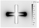
도 4는 도 3에 도시된 도체 패턴 주위에 있어서의 전계 강도의 분포의 시뮬레이션 결과의 일례를 나타낸 도면이다.
도 5는 일 실시형태에 따른 도체 패턴의 확대 평면도이다.
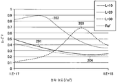
도 6은 도체 패턴의 각 부분의 길이와, 플라즈마의 전자 밀도와, 플라즈마에 대한 마이크로파의 흡수 효율과의 관계의 시뮬레이션 결과의 일례를 나타낸 도면이다.
도 7은 변형례 1에 따른 도체 패턴의 확대 평면도이다.
도 8은 도 7에 도시된 도체 패턴 주위에 있어서의 전계 강도의 분포의 시뮬레이션 결과의 일례를 나타낸 도면이다.
도 9는 변형례 2에 따른 도체 패턴의 확대 평면도이다.
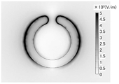
도 10은 도 9에 도시된 도체 패턴 주위에 있어서의 전계 강도의 분포의 시뮬레이션 결과의 일례를 나타낸 도면이다.
14 : 마이크로파 발생기 15 : 안테나
18 : 유전체창 18a : 대향면
18b : 면 18c : 영역
19 : 도체 패턴 19a : 제1 부분
19b : 제2 부분 20 : 스테이지
36 : 슬롯판 36a : 슬롯
Claims (6)
- 처리 공간을 구획하는 처리 용기와,
플라즈마 여기용의 마이크로파를 발생하는 마이크로파 발생기와,
상기 처리 공간에 대향하는 대향면을 갖는 유전체와,
상기 유전체의 상기 대향면과는 반대측 면 상에 설치되고, 상기 유전체를 통해 상기 마이크로파를 상기 처리 공간으로 방사하는 복수의 슬롯이 형성된 슬롯판과,
상기 유전체의 상기 대향면 상에 형성되고, 각 상기 슬롯으로부터 방사된 상기 마이크로파에 따른 전계를 집중시키는 도체 패턴
을 구비하는 것을 특징으로 하는 플라즈마 처리 장치. - 제1항에 있어서,
상기 도체 패턴은, 상기 유전체의 상기 대향면에 있어서, 상기 대향면에 수직인 방향에서 보았을 경우에 상기 복수의 슬롯과 각각 겹치는 복수의 영역 중, 적어도 어느 하나의 영역에 형성되는 것을 특징으로 하는 플라즈마 처리 장치. - 제1항에 있어서, 상기 도체 패턴의 적어도 일부는 직사각 형상으로 형성되고,
상기 도체 패턴의 적어도 일부의 길이는, 상기 유전체의 내부에서 전파되는 상기 마이크로파의 파장이 λ라고 하면, 3λ/8 이상 5λ/8 이하의 범위 내인 것을 특징으로 하는 플라즈마 처리 장치. - 제3항에 있어서, 상기 도체 패턴의 적어도 일부의 길이는, 상기 마이크로파에 공진하는 길이인 것을 특징으로 하는 플라즈마 처리 장치.
- 제4항에 있어서, 상기 도체 패턴의 적어도 일부의 길이는, λ/2인 것을 특징으로 하는 플라즈마 처리 장치.
- 제1항 내지 제5항 중 어느 한 항에 있어서, 상기 도체 패턴 상에는, 상기 도체 패턴을 플라즈마로부터 보호하기 위한 보호막이 형성되는 것을 특징으로 하는 플라즈마 처리 장치.
Applications Claiming Priority (2)
| Application Number | Priority Date | Filing Date | Title |
|---|---|---|---|
| JP2016028359A JP6695705B2 (ja) | 2016-02-17 | 2016-02-17 | プラズマ処理装置 |
| JPJP-P-2016-028359 | 2016-02-17 |
Publications (2)
| Publication Number | Publication Date |
|---|---|
| KR20170096960A true KR20170096960A (ko) | 2017-08-25 |
| KR102721366B1 KR102721366B1 (ko) | 2024-10-23 |
Family
ID=59559759
Family Applications (1)
| Application Number | Title | Priority Date | Filing Date |
|---|---|---|---|
| KR1020170019956A Active KR102721366B1 (ko) | 2016-02-17 | 2017-02-14 | 플라즈마 처리 장치 |
Country Status (3)
| Country | Link |
|---|---|
| US (1) | US10546725B2 (ko) |
| JP (1) | JP6695705B2 (ko) |
| KR (1) | KR102721366B1 (ko) |
Families Citing this family (9)
| Publication number | Priority date | Publication date | Assignee | Title |
|---|---|---|---|---|
| JP6804280B2 (ja) * | 2016-12-07 | 2020-12-23 | 東京エレクトロン株式会社 | プラズマ処理装置及びプラズマ処理方法 |
| JP7250376B2 (ja) * | 2017-07-28 | 2023-04-03 | ヤマハファインテック株式会社 | ガス漏れ検査システム及びガス漏れ検査方法 |
| JP2022039820A (ja) | 2020-08-28 | 2022-03-10 | 東京エレクトロン株式会社 | プラズマ処理装置およびプラズマ処理方法 |
| WO2022157883A1 (ja) * | 2021-01-21 | 2022-07-28 | 株式会社日立ハイテク | プラズマ処理装置 |
| WO2023032725A1 (ja) * | 2021-09-03 | 2023-03-09 | 東京エレクトロン株式会社 | プラズマ処理装置及びプラズマ制御方法 |
| JP7772325B2 (ja) * | 2022-06-09 | 2025-11-18 | 東京エレクトロン株式会社 | プラズマ処理装置及び共振周波数測定方法 |
| CN115821215B (zh) * | 2023-02-20 | 2023-04-28 | 成都富林达新材料有限公司 | 一种用于悬浮蒸镀氧化铝的喷射装置 |
| JP2024147876A (ja) * | 2023-04-04 | 2024-10-17 | 東京エレクトロン株式会社 | プラズマ処理装置 |
| JP2025055372A (ja) * | 2023-09-27 | 2025-04-08 | 東京エレクトロン株式会社 | プラズマ処理装置 |
Citations (5)
| Publication number | Priority date | Publication date | Assignee | Title |
|---|---|---|---|---|
| JPH0963794A (ja) * | 1995-06-15 | 1997-03-07 | Sumitomo Metal Ind Ltd | マイクロ波プラズマ処理装置 |
| JP2000273646A (ja) * | 1999-03-24 | 2000-10-03 | Sumitomo Metal Ind Ltd | マイクロ波プラズマ処理装置 |
| JP2004014262A (ja) * | 2002-06-06 | 2004-01-15 | Tokyo Electron Ltd | プラズマ処理装置 |
| JP2004235434A (ja) * | 2003-01-30 | 2004-08-19 | Rohm Co Ltd | プラズマ処理装置 |
| JP2015188061A (ja) | 2014-03-11 | 2015-10-29 | 東京エレクトロン株式会社 | プラズマ処理装置及び成膜方法 |
Family Cites Families (4)
| Publication number | Priority date | Publication date | Assignee | Title |
|---|---|---|---|---|
| US6998565B2 (en) * | 2003-01-30 | 2006-02-14 | Rohm Co., Ltd. | Plasma processing apparatus |
| JP4910396B2 (ja) * | 2006-01-12 | 2012-04-04 | 東京エレクトロン株式会社 | プラズマ処理装置 |
| US7998307B2 (en) * | 2006-09-12 | 2011-08-16 | Tokyo Electron Limited | Electron beam enhanced surface wave plasma source |
| US20100078315A1 (en) * | 2008-09-26 | 2010-04-01 | Applied Materials, Inc. | Microstrip antenna assisted ipvd |
-
2016
- 2016-02-17 JP JP2016028359A patent/JP6695705B2/ja active Active
-
2017
- 2017-02-10 US US15/429,393 patent/US10546725B2/en active Active
- 2017-02-14 KR KR1020170019956A patent/KR102721366B1/ko active Active
Patent Citations (5)
| Publication number | Priority date | Publication date | Assignee | Title |
|---|---|---|---|---|
| JPH0963794A (ja) * | 1995-06-15 | 1997-03-07 | Sumitomo Metal Ind Ltd | マイクロ波プラズマ処理装置 |
| JP2000273646A (ja) * | 1999-03-24 | 2000-10-03 | Sumitomo Metal Ind Ltd | マイクロ波プラズマ処理装置 |
| JP2004014262A (ja) * | 2002-06-06 | 2004-01-15 | Tokyo Electron Ltd | プラズマ処理装置 |
| JP2004235434A (ja) * | 2003-01-30 | 2004-08-19 | Rohm Co Ltd | プラズマ処理装置 |
| JP2015188061A (ja) | 2014-03-11 | 2015-10-29 | 東京エレクトロン株式会社 | プラズマ処理装置及び成膜方法 |
Also Published As
| Publication number | Publication date |
|---|---|
| JP2017147129A (ja) | 2017-08-24 |
| KR102721366B1 (ko) | 2024-10-23 |
| US20170236690A1 (en) | 2017-08-17 |
| US10546725B2 (en) | 2020-01-28 |
| JP6695705B2 (ja) | 2020-05-20 |
Similar Documents
| Publication | Publication Date | Title |
|---|---|---|
| KR20170096960A (ko) | 플라즈마 처리 장치 | |
| TWI681073B (zh) | 電漿處理裝置 | |
| KR100494607B1 (ko) | 플라즈마 프로세스 장치 | |
| JP3483147B2 (ja) | マイクロ波プラズマ反応器 | |
| KR101266890B1 (ko) | 플라즈마 처리 장치 및 플라즈마 처리 방법 | |
| JP5082229B2 (ja) | プラズマ処理装置 | |
| US5556475A (en) | Microwave plasma reactor | |
| JP5438260B2 (ja) | プラズマ処理装置 | |
| US9646867B2 (en) | Plasma processing apparatus, power supply unit and mounting table system | |
| KR20120112261A (ko) | 플라즈마 처리 장치 및 플라즈마 발생용 안테나 | |
| KR102605240B1 (ko) | 플라스마 처리 장치 및 플라스마 처리 방법 | |
| KR101274515B1 (ko) | 플라즈마 처리장치 | |
| KR102690756B1 (ko) | 플라즈마 처리 장치 및 프리코팅 처리 방법 | |
| JP5522887B2 (ja) | プラズマ処理装置 | |
| KR100794806B1 (ko) | 플라즈마 처리 장치 및 방법과, 슬롯 안테나 | |
| JP5723397B2 (ja) | プラズマ処理装置 | |
| KR100984121B1 (ko) | 기판처리장치 및 방법 | |
| TW201411688A (zh) | 電漿處理裝置及電漿處理方法 | |
| KR20110082193A (ko) | 플라즈마 처리 장치 | |
| CN114514794B (zh) | 具有集成温度控制的单片式模块化微波源 | |
| US12362147B2 (en) | Apparatus for treating substrate | |
| US20190279845A1 (en) | Antenna device and plasma processing apparatus | |
| KR20170093723A (ko) | 플라즈마 처리 장치 | |
| KR20210091338A (ko) | 플라스마 처리 장치 및 플라스마 처리 방법 | |
| US20250210316A1 (en) | Substrate processing apparatus using microwaves |
Legal Events
| Date | Code | Title | Description |
|---|---|---|---|
| PA0109 | Patent application |
Patent event code: PA01091R01D Comment text: Patent Application Patent event date: 20170214 |
|
| PG1501 | Laying open of application | ||
| A201 | Request for examination | ||
| PA0201 | Request for examination |
Patent event code: PA02012R01D Patent event date: 20211115 Comment text: Request for Examination of Application Patent event code: PA02011R01I Patent event date: 20170214 Comment text: Patent Application |
|
| E902 | Notification of reason for refusal | ||
| PE0902 | Notice of grounds for rejection |
Comment text: Notification of reason for refusal Patent event date: 20240425 Patent event code: PE09021S01D |
|
| E701 | Decision to grant or registration of patent right | ||
| PE0701 | Decision of registration |
Patent event code: PE07011S01D Comment text: Decision to Grant Registration Patent event date: 20240724 |
|
| GRNT | Written decision to grant | ||
| PR0701 | Registration of establishment |
Comment text: Registration of Establishment Patent event date: 20241021 Patent event code: PR07011E01D |
|
| PR1002 | Payment of registration fee |
Payment date: 20241021 End annual number: 3 Start annual number: 1 |
|
| PG1601 | Publication of registration |