KR20170097501A - Awg 플랫폼 기반 초소형 광 트랜시버 - Google Patents
Awg 플랫폼 기반 초소형 광 트랜시버 Download PDFInfo
- Publication number
- KR20170097501A KR20170097501A KR1020160019343A KR20160019343A KR20170097501A KR 20170097501 A KR20170097501 A KR 20170097501A KR 1020160019343 A KR1020160019343 A KR 1020160019343A KR 20160019343 A KR20160019343 A KR 20160019343A KR 20170097501 A KR20170097501 A KR 20170097501A
- Authority
- KR
- South Korea
- Prior art keywords
- trench
- waveguide
- awg
- platform
- optical transceiver
- Prior art date
- Legal status (The legal status is an assumption and is not a legal conclusion. Google has not performed a legal analysis and makes no representation as to the accuracy of the status listed.)
- Granted
Links
- 230000003287 optical effect Effects 0.000 title claims abstract description 48
- 238000000034 method Methods 0.000 claims description 5
- 238000004519 manufacturing process Methods 0.000 description 8
- 238000010586 diagram Methods 0.000 description 7
- 238000007796 conventional method Methods 0.000 description 2
- 238000005516 engineering process Methods 0.000 description 2
- 238000003491 array Methods 0.000 description 1
- 230000008878 coupling Effects 0.000 description 1
- 238000010168 coupling process Methods 0.000 description 1
- 238000005859 coupling reaction Methods 0.000 description 1
- 238000005530 etching Methods 0.000 description 1
- 238000007639 printing Methods 0.000 description 1
- 230000003252 repetitive effect Effects 0.000 description 1
Images





Classifications
-
- G—PHYSICS
- G02—OPTICS
- G02B—OPTICAL ELEMENTS, SYSTEMS OR APPARATUS
- G02B6/00—Light guides; Structural details of arrangements comprising light guides and other optical elements, e.g. couplings
- G02B6/10—Light guides; Structural details of arrangements comprising light guides and other optical elements, e.g. couplings of the optical waveguide type
- G02B6/12—Light guides; Structural details of arrangements comprising light guides and other optical elements, e.g. couplings of the optical waveguide type of the integrated circuit kind
- G02B6/12007—Light guides; Structural details of arrangements comprising light guides and other optical elements, e.g. couplings of the optical waveguide type of the integrated circuit kind forming wavelength selective elements, e.g. multiplexer, demultiplexer
- G02B6/12009—Light guides; Structural details of arrangements comprising light guides and other optical elements, e.g. couplings of the optical waveguide type of the integrated circuit kind forming wavelength selective elements, e.g. multiplexer, demultiplexer comprising arrayed waveguide grating [AWG] devices, i.e. with a phased array of waveguides
-
- G—PHYSICS
- G02—OPTICS
- G02B—OPTICAL ELEMENTS, SYSTEMS OR APPARATUS
- G02B6/00—Light guides; Structural details of arrangements comprising light guides and other optical elements, e.g. couplings
- G02B6/24—Coupling light guides
- G02B6/42—Coupling light guides with opto-electronic elements
- G02B6/4201—Packages, e.g. shape, construction, internal or external details
- G02B6/4246—Bidirectionally operating package structures
-
- H—ELECTRICITY
- H04—ELECTRIC COMMUNICATION TECHNIQUE
- H04B—TRANSMISSION
- H04B10/00—Transmission systems employing electromagnetic waves other than radio-waves, e.g. infrared, visible or ultraviolet light, or employing corpuscular radiation, e.g. quantum communication
- H04B10/40—Transceivers
Landscapes
- Physics & Mathematics (AREA)
- Engineering & Computer Science (AREA)
- General Physics & Mathematics (AREA)
- Optics & Photonics (AREA)
- Microelectronics & Electronic Packaging (AREA)
- Electromagnetism (AREA)
- Computer Networks & Wireless Communication (AREA)
- Signal Processing (AREA)
- Optical Couplings Of Light Guides (AREA)
- Semiconductor Lasers (AREA)
Abstract
Description
도 1b는 기존 광트랜시버에 있어서 광케이블과 LD를 정렬하는 기존 기술 중의 또 하나를 개략적으로 표현한 도면이다.
도 1c는 기존 광트랜시버에 있어서 광케이블과 LD를 정렬하는 기존 기술 중의 또 하나를 개략적으로 표현한 도면이다.
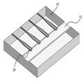
도 2a는 본 발명에 따른 AWG 플랫폼 기반 광 트랜시버가 제작될 때에 있어서 AWG에 트렌치가 파이고 평면렌즈가 장착된 것을 나타낸 도면이다.
도 2b는 테이퍼 형태의 평면 렌즈가 AWG에 장착된 것을 나타낸 평면 단면도이다.
도 2c는 도 2a의 장치에 전극이 프린팅된 것을 나타낸 도면이다.
도 2d는 도 2c의 장치에 신호 발광 영역을 아래로 한 LD가 실장하여 신호 발광 영역과 평면 렌즈가 정렬 된 것을 나타낸 도면이다.
도 2e는 도 2d의 장치에 LD 드라이버를 실장한 것을 나타낸 도면이다.
도 3a는 도 2e의 장치의 평면도이다.
도 3b는 도 2e의 장치의 수직 단면도이다.
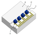
도 4a는 본 발명에 따른 AWG 플랫폼 기반 광 트랜시버가 완성된 것으로서 싱글 LD 칩이 실장된 것을 나타낸 도면이다.
도 4b는 본 발명에 따른 AWG 플랫폼 기반 광 트랜시버가 완성된 것으로서 LD 어레이가 실장된 것을 나타낸 도면이다.
20 : 도파로 30 : 전극
40 : LD 40a : 단일 LD 칩
40b : LD 칩 어레이 45 : 신호 발광 영역
50 : LD 드라이버
Claims (4)
- AWG 플랫폼 기반의 광트랜시버에 있어서,
상기 광트랜시버는,
AWG를 이루는 플랫폼에 트랜치가 파이고 상기 트랜치에 전극이 형성되고 연장되어 외부 전원과 연결되고, 트랜치에 형성된 전극 위로 LD가 신호 발광 영역을 아래로 하여 실장되고, 트랜치 외부로 연장 연결된 전극 위로 LD 드라이버 소자가 실장되며, 상기 플랫폼 내부에는 도파로가 설치되어 있으되, 트랜치를 이루는 하나의 측면에 상기 도파로 말단이 노출되어 있으며,
상기 트랜치의 깊이는 상기 전극의 두께와 도파로 두께를 합한 길이를 초과하며,
실장된 LD의 신호 발광 영역이 상기 트랜치를 이루는 하나의 측면에 노출된 도파로 말단과 대응되어 광신호를 주고 받을 수 있음을 특징으로 하는 AWG 플랫폼 기반 초소형 광트랜시버. - 청구항 1에 있어서,
상기 트랜치를 이루는 하나의 측면에 노출된 도파로 말단은 평면으로 볼록하게 원형을 이루어 평면 볼록 렌즈 형태를 가지는 것을 특징으로 하는 AWG 플랫폼 기반 초소형 광트랜시버. - 청구항 1에 있어서,
상기 도파로는 트렌치 측면에 노출된 말단부 방향으로 넓어져 테이퍼 형태를 이루는 것을 특징으로 하는 AWG 플랫폼 기반 초소형 광트랜시버. - 청구항 1에 있어서,
실장되는 LD는 광트랜시버의 신호 채널 수에 따라 단일 LD 칩이 여러개 또는 신호 채널수에 대응하는 LD 칩 어레이가 실장되는 것을 특징으로 하는 AWG 플랫폼 기반 초소형 광트랜시버.
Priority Applications (1)
| Application Number | Priority Date | Filing Date | Title |
|---|---|---|---|
| KR1020160019343A KR101827715B1 (ko) | 2016-02-18 | 2016-02-18 | Awg 플랫폼 기반 초소형 광 트랜시버 |
Applications Claiming Priority (1)
| Application Number | Priority Date | Filing Date | Title |
|---|---|---|---|
| KR1020160019343A KR101827715B1 (ko) | 2016-02-18 | 2016-02-18 | Awg 플랫폼 기반 초소형 광 트랜시버 |
Publications (2)
| Publication Number | Publication Date |
|---|---|
| KR20170097501A true KR20170097501A (ko) | 2017-08-28 |
| KR101827715B1 KR101827715B1 (ko) | 2018-02-09 |
Family
ID=59759744
Family Applications (1)
| Application Number | Title | Priority Date | Filing Date |
|---|---|---|---|
| KR1020160019343A Active KR101827715B1 (ko) | 2016-02-18 | 2016-02-18 | Awg 플랫폼 기반 초소형 광 트랜시버 |
Country Status (1)
| Country | Link |
|---|---|
| KR (1) | KR101827715B1 (ko) |
Cited By (3)
| Publication number | Priority date | Publication date | Assignee | Title |
|---|---|---|---|---|
| CN107688216A (zh) * | 2017-10-10 | 2018-02-13 | 成都优博创通信技术股份有限公司 | 光接收模块和光通信系统 |
| KR101896632B1 (ko) | 2017-09-28 | 2018-09-07 | 엑스빔테크 주식회사 | 광 트랜시버 모듈 |
| CN112817102A (zh) * | 2021-01-04 | 2021-05-18 | 武汉光迅科技股份有限公司 | 一种光模块及其制备方法 |
Family Cites Families (1)
| Publication number | Priority date | Publication date | Assignee | Title |
|---|---|---|---|---|
| JP4845851B2 (ja) * | 2007-10-23 | 2011-12-28 | 日東電工株式会社 | タッチパネル用光導波路およびそれを用いたタッチパネル |
-
2016
- 2016-02-18 KR KR1020160019343A patent/KR101827715B1/ko active Active
Cited By (3)
| Publication number | Priority date | Publication date | Assignee | Title |
|---|---|---|---|---|
| KR101896632B1 (ko) | 2017-09-28 | 2018-09-07 | 엑스빔테크 주식회사 | 광 트랜시버 모듈 |
| CN107688216A (zh) * | 2017-10-10 | 2018-02-13 | 成都优博创通信技术股份有限公司 | 光接收模块和光通信系统 |
| CN112817102A (zh) * | 2021-01-04 | 2021-05-18 | 武汉光迅科技股份有限公司 | 一种光模块及其制备方法 |
Also Published As
| Publication number | Publication date |
|---|---|
| KR101827715B1 (ko) | 2018-02-09 |
Similar Documents
| Publication | Publication Date | Title |
|---|---|---|
| KR100583646B1 (ko) | 병렬 광접속 모듈용 광접속 장치 및 이를 이용한 병렬광접속 모듈 | |
| CN203385897U (zh) | 具有柔性印刷电路板的高速光学模块 | |
| US9435970B2 (en) | Optical connector | |
| US6874952B2 (en) | Optical module and method of assembling the optical module | |
| EP2300862B1 (en) | Optical communication module for optical wavelength division multiplexing | |
| JP5737254B2 (ja) | 光通信モジュール | |
| KR100627701B1 (ko) | 병렬 광접속 모듈 | |
| KR101827715B1 (ko) | Awg 플랫폼 기반 초소형 광 트랜시버 | |
| TWI483023B (zh) | Socket and optical transmission module | |
| JPWO2019012607A1 (ja) | 光モジュール | |
| CN116184583A (zh) | 一种自对准光纤的400g硅光封装结构 | |
| EP2613188A1 (en) | Optical transmission substrate, optical transmission module, and method for manufacturing optical transmission substrate | |
| US20040218874A1 (en) | Fiber optic transceiver module, manufacturing method thereof, and electronic equipment | |
| JP4983149B2 (ja) | 光送信器 | |
| WO2014030562A1 (ja) | レセプタクル及び光伝送モジュール | |
| JP2009199037A (ja) | 光モジュール | |
| US6312167B1 (en) | Light transmission module | |
| US9103971B2 (en) | Optical module and method for producing the same | |
| JP5614725B2 (ja) | 光モジュール | |
| JPH08160262A (ja) | 光コネクタ | |
| JPH0339706A (ja) | 光モジュール | |
| KR102356288B1 (ko) | 광 결합 장치 | |
| JP2008134444A (ja) | 光モジュール及び光導波路構造体 | |
| KR100258962B1 (ko) | 광전송 모듈 | |
| JP5664910B2 (ja) | 光モジュール |
Legal Events
| Date | Code | Title | Description |
|---|---|---|---|
| A201 | Request for examination | ||
| PA0109 | Patent application |
Patent event code: PA01091R01D Comment text: Patent Application Patent event date: 20160218 |
|
| PA0201 | Request for examination | ||
| E902 | Notification of reason for refusal | ||
| PE0902 | Notice of grounds for rejection |
Comment text: Notification of reason for refusal Patent event date: 20170710 Patent event code: PE09021S01D |
|
| PG1501 | Laying open of application | ||
| E701 | Decision to grant or registration of patent right | ||
| PE0701 | Decision of registration |
Patent event code: PE07011S01D Comment text: Decision to Grant Registration Patent event date: 20180122 |
|
| GRNT | Written decision to grant | ||
| PR0701 | Registration of establishment |
Comment text: Registration of Establishment Patent event date: 20180205 Patent event code: PR07011E01D |
|
| PR1002 | Payment of registration fee |
Payment date: 20180205 End annual number: 3 Start annual number: 1 |
|
| PG1601 | Publication of registration | ||
| PR1001 | Payment of annual fee |
Payment date: 20220126 Start annual number: 5 End annual number: 5 |
|
| PR1001 | Payment of annual fee |
Payment date: 20230131 Start annual number: 6 End annual number: 6 |
|
| PR1001 | Payment of annual fee |
Payment date: 20231130 Start annual number: 7 End annual number: 7 |
|
| PR1001 | Payment of annual fee |
Payment date: 20241128 Start annual number: 8 End annual number: 8 |