KR20170097650A - 미러 디바이스 - Google Patents
미러 디바이스 Download PDFInfo
- Publication number
- KR20170097650A KR20170097650A KR1020177016251A KR20177016251A KR20170097650A KR 20170097650 A KR20170097650 A KR 20170097650A KR 1020177016251 A KR1020177016251 A KR 1020177016251A KR 20177016251 A KR20177016251 A KR 20177016251A KR 20170097650 A KR20170097650 A KR 20170097650A
- Authority
- KR
- South Korea
- Prior art keywords
- mirror
- shielding
- mirror device
- electrically conductive
- mirrors
- Prior art date
- Legal status (The legal status is an assumption and is not a legal conclusion. Google has not performed a legal analysis and makes no representation as to the accuracy of the status listed.)
- Granted
Links
Images




Classifications
-
- G—PHYSICS
- G02—OPTICS
- G02B—OPTICAL ELEMENTS, SYSTEMS OR APPARATUS
- G02B5/00—Optical elements other than lenses
- G02B5/08—Mirrors
- G02B5/09—Multifaceted or polygonal mirrors, e.g. polygonal scanning mirrors; Fresnel mirrors
-
- G—PHYSICS
- G02—OPTICS
- G02B—OPTICAL ELEMENTS, SYSTEMS OR APPARATUS
- G02B5/00—Optical elements other than lenses
- G02B5/08—Mirrors
-
- G—PHYSICS
- G03—PHOTOGRAPHY; CINEMATOGRAPHY; ANALOGOUS TECHNIQUES USING WAVES OTHER THAN OPTICAL WAVES; ELECTROGRAPHY; HOLOGRAPHY
- G03F—PHOTOMECHANICAL PRODUCTION OF TEXTURED OR PATTERNED SURFACES, e.g. FOR PRINTING, FOR PROCESSING OF SEMICONDUCTOR DEVICES; MATERIALS THEREFOR; ORIGINALS THEREFOR; APPARATUS SPECIALLY ADAPTED THEREFOR
- G03F7/00—Photomechanical, e.g. photolithographic, production of textured or patterned surfaces, e.g. printing surfaces; Materials therefor, e.g. comprising photoresists; Apparatus specially adapted therefor
- G03F7/70—Microphotolithographic exposure; Apparatus therefor
- G03F7/70058—Mask illumination systems
- G03F7/70075—Homogenization of illumination intensity in the mask plane by using an integrator, e.g. fly's eye lens, facet mirror or glass rod, by using a diffusing optical element or by beam deflection
-
- G—PHYSICS
- G03—PHOTOGRAPHY; CINEMATOGRAPHY; ANALOGOUS TECHNIQUES USING WAVES OTHER THAN OPTICAL WAVES; ELECTROGRAPHY; HOLOGRAPHY
- G03F—PHOTOMECHANICAL PRODUCTION OF TEXTURED OR PATTERNED SURFACES, e.g. FOR PRINTING, FOR PROCESSING OF SEMICONDUCTOR DEVICES; MATERIALS THEREFOR; ORIGINALS THEREFOR; APPARATUS SPECIALLY ADAPTED THEREFOR
- G03F7/00—Photomechanical, e.g. photolithographic, production of textured or patterned surfaces, e.g. printing surfaces; Materials therefor, e.g. comprising photoresists; Apparatus specially adapted therefor
- G03F7/70—Microphotolithographic exposure; Apparatus therefor
- G03F7/70058—Mask illumination systems
- G03F7/70091—Illumination settings, i.e. intensity distribution in the pupil plane or angular distribution in the field plane; On-axis or off-axis settings, e.g. annular, dipole or quadrupole settings; Partial coherence control, i.e. sigma or numerical aperture [NA]
- G03F7/70116—Off-axis setting using a programmable means, e.g. liquid crystal display [LCD], digital micromirror device [DMD] or pupil facets
-
- G—PHYSICS
- G03—PHOTOGRAPHY; CINEMATOGRAPHY; ANALOGOUS TECHNIQUES USING WAVES OTHER THAN OPTICAL WAVES; ELECTROGRAPHY; HOLOGRAPHY
- G03F—PHOTOMECHANICAL PRODUCTION OF TEXTURED OR PATTERNED SURFACES, e.g. FOR PRINTING, FOR PROCESSING OF SEMICONDUCTOR DEVICES; MATERIALS THEREFOR; ORIGINALS THEREFOR; APPARATUS SPECIALLY ADAPTED THEREFOR
- G03F7/00—Photomechanical, e.g. photolithographic, production of textured or patterned surfaces, e.g. printing surfaces; Materials therefor, e.g. comprising photoresists; Apparatus specially adapted therefor
- G03F7/70—Microphotolithographic exposure; Apparatus therefor
- G03F7/70058—Mask illumination systems
- G03F7/702—Reflective illumination, i.e. reflective optical elements other than folding mirrors, e.g. extreme ultraviolet [EUV] illumination systems
-
- G—PHYSICS
- G03—PHOTOGRAPHY; CINEMATOGRAPHY; ANALOGOUS TECHNIQUES USING WAVES OTHER THAN OPTICAL WAVES; ELECTROGRAPHY; HOLOGRAPHY
- G03F—PHOTOMECHANICAL PRODUCTION OF TEXTURED OR PATTERNED SURFACES, e.g. FOR PRINTING, FOR PROCESSING OF SEMICONDUCTOR DEVICES; MATERIALS THEREFOR; ORIGINALS THEREFOR; APPARATUS SPECIALLY ADAPTED THEREFOR
- G03F7/00—Photomechanical, e.g. photolithographic, production of textured or patterned surfaces, e.g. printing surfaces; Materials therefor, e.g. comprising photoresists; Apparatus specially adapted therefor
- G03F7/70—Microphotolithographic exposure; Apparatus therefor
- G03F7/708—Construction of apparatus, e.g. environment aspects, hygiene aspects or materials
- G03F7/70908—Hygiene, e.g. preventing apparatus pollution, mitigating effect of pollution or removing pollutants from apparatus
Landscapes
- Physics & Mathematics (AREA)
- General Physics & Mathematics (AREA)
- Health & Medical Sciences (AREA)
- Epidemiology (AREA)
- Public Health (AREA)
- Optics & Photonics (AREA)
- Life Sciences & Earth Sciences (AREA)
- Atmospheric Sciences (AREA)
- Engineering & Computer Science (AREA)
- Environmental & Geological Engineering (AREA)
- Exposure And Positioning Against Photoresist Photosensitive Materials (AREA)
- Exposure Of Semiconductors, Excluding Electron Or Ion Beam Exposure (AREA)
Abstract
Description
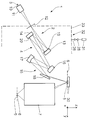
도 1은 마이크로리소그래피 투영 노광 장치의 개략도를 도시한다.
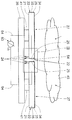
도 2는 두 개의 인접한 개별 미러의 구역에서 다중-미러 어레이의 단면 모습의 세부사항의 개략도를 도시한다.
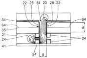
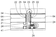
도 3a 및 도 3b는 개별 미러의 변위를 위한 액추에이터의 동작의 다양한 상태에서의 전기 필드의 필드 라인(field line) 패턴의 예시적 모습과 함께 도 2로부터의 구역(Ⅲ)의 세부사항의 확대도를 도시한다.
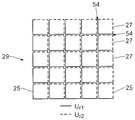
도 4는 인접한 개별 미러들의 측부 표면의 구역에서 차폐 전극의 쌍의 배열의 예시를 위한 다중-미러 어레이의 평면도로부터의 세부사항을 간략하게 도시한다.
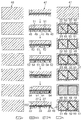
도 5는 개별 미러를 생성하기 위한 방법의 경우 중간 생성물의 시퀀스의 위로부터의(좌측 열), 아래로부터의(우측 열), 그리고 수직 단면(중간 열)의 도면을 간략하게 도시한다.
도 6은 보유 핀을 생성하기 위한 방법의 경우에 도 5에 대응하는 도면을 도시한다.
도 7은 도 5에서 도시된 바와 같은 미러 및 도 6에서 도시된 바와 같은 보유 핀으로부터 조립된 미러 요소를 생성하기 위한 방법의 경우에 도 5 및 도 6에 대응하는 도면을 도시한다.
도 8은 도 7에 도시된 바와 같은 조립된 미러로부터 다중-미러 어레이를 생성하기 위한 방법의 경우에 중간 생성물을 통한 수직 단면의 도면을 도시한다.
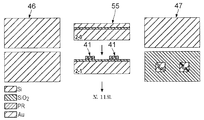
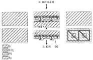
도 9 내지 도 12는 대안례에 따라 도 5 내지 도 8에 도시된 바와 같은 도면을 도시한다.
도 13은 차폐 요소의 대안적인 실시예의 도 2에 도시된 바와 같은 도면을 도시한다.
도 14는 도 13에 도시된 바와 같은 차폐 요소의 동작의 경우에 전기 필드의 필드 라인의 예시적인 패턴의 도면을 도시한다.


Claims (14)
- 미러 디바이스(29)이며,
1.1. 미러 본체(35)를 가지는 적어도 하나의 미러(27)로서,
1.1.1. 전방으로 향하는 전방 측부,
1.1.2. 후방 측부(21), 그리고
1.1.3. 적어도 하나의 측부 표면(22)
을 가지는 미러, 및
1.2. 적어도 두 개의 전기 전도성 차폐 요소(25)로서,
1.2.1. 적어도 두 개의 전기 공급 라인(64)에 의해 상이한 전압(Ur1, Ur2)이 차폐 요소에 적용될 수 있고;
1.2.2. 적어도 하나의 측부 표면(22) 및/또는 후방 측부(21)에 인접한 구역에 전기 필드를 생성하기 위한 수단을 형성하는
전기 전도성 차폐 요소
를 포함하는 미러 디바이스. - 제1항에 있어서, 전기 전도성 차폐 요소(25) 중 적어도 하나는 미러(27)의 적어도 하나의 측부 표면(22)의 구역 및/또는 후방 측부(21) 상의 또는 그 뒤의 구역에 배열되는 것을 특징으로 하는 미러 디바이스(29).
- 제1항 또는 제2항에 있어서, 전기 전도성 차폐 요소(25) 중 적어도 하나에 -300V 내지 300V 범위의 전기 전압을 적용시키기 위한 전압 소스(63)를 특징으로 하는 미러 디바이스(29).
- 제1항 내지 제3항 중 어느 한 항에 있어서, 전기 전도성 차폐 요소(25) 중 적어도 하나에 적용된 전기 전압을 제어하기 위한 제어 디바이스(60)를 특징으로 하는 미러 디바이스(29).
- 제1항 내지 제4항 중 어느 한 항에 있어서, 전압(Ur1, Ur2)이 미러 본체(35)의 전기 공급 라인에 의해 차폐 요소(25)에 적용될 수 있는 것을 특징으로 하는 미러 디바이스(29).
- 제1항 내지 제5항 중 어느 한 항에 있어서, 적어도 두 개의 전기 전도성 차폐 요소(25)가 미러 본체(35) 중 하나의 상이한 측부 표면(22)에 또는 그 상에 배열되는 것을 특징으로 하는 미러 디바이스(29).
- 제1항 내지 제6항 중 어느 한 항에 있어서, 제1항 내지 제6항 중 어느 한 항에서 청구된 바와 같은 복수의 미러(27)를 특징으로 하는 미러 디바이스(29).
- 제7항에 있어서, 적어도 하나의 전기 전도성 차폐 요소(25)가 두 인접한 미러(27) 사이의 사이공간 뒤의 구역에 각각 배열되는 것을 특징으로 하는 미러 디바이스(29).
- 제7항 또는 제8항에 있어서, 두 전기 전도성 차폐 요소(25)는 인접한 미러(27)들의 상호 대향하는 측부 표면(22)의 구역에 쌍으로 각각 배열되는 것을 특징으로 하는 미러 디바이스(29).
- 투영 노광 장치(1)를 위한 조명 광학 유닛(4)이며, 제1항 내지 제9항 중 어느 한 항에 청구된 바와 같은 적어도 하나의 미러 디바이스(29)를 포함하는 조명 광학 유닛.
- 마이크로리소그래피 투영 노광 장치(1)를 위한 조명 시스템(2)이며,
11.1. 제10항에서 청구된 바와 같은 조명 광학 유닛(4) 그리고
11.2. 조명 방사선(10)을 발생시키기 위한 방사선 소스(3)
를 포함하는 마이크로리소그래피 투영 노광 장치. - 마이크로리소그래피 투영 노광 장치(1)이며,
12.1. 제10항에서 청구된 바와 같은 조명 광학 유닛(4) 그리고
12.2. 대물 필드(5)로부터 영상 필드(8) 내로 조명 방사선(10)을 투영시키기 위한 투영 광학 유닛(7)
을 포함하는 마이크로리소그래피 투영 노광 장치. - 마이크로 또는 나노구조화된 구성요소를 생성하는 방법이며,
13.1. 레티클(30)을 제공하는 단계,
13.2. 조명 방사선(10)에 민감한 코팅을 가지는 웨이퍼를 제공하는 단계,
13.3. 제12항에 청구된 바와 같은 투영 노광 장치(1)의 도움에 의해 웨이퍼 상으로 레티클(30)의 적어도 하나의 섹션을 투영하는 단계, 및
13.4. 조명 방사선(10)에 의해 노광된 웨이퍼 상에 감광층을 현상하는 단계
를 포함하는 방법. - 제13항에 청구된 바와 같은 방법에 따라 생성된 구성요소.
Applications Claiming Priority (3)
| Application Number | Priority Date | Filing Date | Title |
|---|---|---|---|
| DE102014226272.0 | 2014-12-17 | ||
| DE102014226272.0A DE102014226272A1 (de) | 2014-12-17 | 2014-12-17 | Spiegel-Einrichtung |
| PCT/EP2015/079829 WO2016096878A1 (de) | 2014-12-17 | 2015-12-15 | Spiegel-einrichtung |
Publications (2)
| Publication Number | Publication Date |
|---|---|
| KR20170097650A true KR20170097650A (ko) | 2017-08-28 |
| KR102549920B1 KR102549920B1 (ko) | 2023-07-03 |
Family
ID=54937052
Family Applications (1)
| Application Number | Title | Priority Date | Filing Date |
|---|---|---|---|
| KR1020177016251A Active KR102549920B1 (ko) | 2014-12-17 | 2015-12-15 | 미러 디바이스 |
Country Status (6)
| Country | Link |
|---|---|
| US (1) | US10101507B2 (ko) |
| EP (1) | EP3234695B1 (ko) |
| KR (1) | KR102549920B1 (ko) |
| CN (1) | CN107111246B (ko) |
| DE (1) | DE102014226272A1 (ko) |
| WO (1) | WO2016096878A1 (ko) |
Families Citing this family (5)
| Publication number | Priority date | Publication date | Assignee | Title |
|---|---|---|---|---|
| DE102016216188A1 (de) | 2016-08-29 | 2018-03-01 | Carl Zeiss Smt Gmbh | Steuereinrichtung |
| DE102017213181A1 (de) * | 2017-07-31 | 2019-01-31 | Carl Zeiss Smt Gmbh | Optische Anordnung für EUV-Strahlung mit einer Abschirmung zum Schutz vor der Ätzwirkung eines Plasmas |
| DE102020205123A1 (de) * | 2020-04-23 | 2021-10-28 | Carl Zeiss Smt Gmbh | Facetten-Baugruppe für einen Facettenspiegel |
| DE102022213753A1 (de) | 2022-05-04 | 2023-11-09 | Carl Zeiss Smt Gmbh | Vorrichtung zum Schutz einer Oberfläche vor Schädigung durch auftreffende Ionen |
| DE102022209411A1 (de) * | 2022-09-09 | 2024-03-14 | Carl Zeiss Smt Gmbh | Mikrospiegelanordnung mit einer Anzahl von Einzelspiegelelementen |
Citations (3)
| Publication number | Priority date | Publication date | Assignee | Title |
|---|---|---|---|---|
| KR960038440A (ko) * | 1995-04-28 | 1996-11-21 | 제프리 엘.포만 | 공간 광 변조기 어레이 및 공간 광 변조기 어레이 형성방법 |
| US20020096647A1 (en) * | 2000-08-25 | 2002-07-25 | Asm Lithography B.V. | Mask handling apparatus, lithographic projection apparatus, device manufacturing method and device manufactured thereby |
| WO2009100856A1 (en) * | 2008-02-15 | 2009-08-20 | Carl Zeiss Smt Ag | Facet mirror for use in a projection exposure apparatus for microlithography |
Family Cites Families (8)
| Publication number | Priority date | Publication date | Assignee | Title |
|---|---|---|---|---|
| DE10138313A1 (de) | 2001-01-23 | 2002-07-25 | Zeiss Carl | Kollektor für Beleuchtugnssysteme mit einer Wellenlänge < 193 nm |
| JP3912760B2 (ja) * | 1999-01-20 | 2007-05-09 | 富士フイルム株式会社 | アレイ型光変調素子の駆動方法、並びに平面表示装置 |
| US7719661B2 (en) * | 2007-11-27 | 2010-05-18 | Nikon Corporation | Illumination optical apparatus, exposure apparatus, and method for producing device |
| JP5355699B2 (ja) | 2008-10-20 | 2013-11-27 | カール・ツァイス・エスエムティー・ゲーエムベーハー | 放射線ビームを案内するための光学モジュール |
| WO2010049976A1 (ja) | 2008-10-31 | 2010-05-06 | 三菱電機株式会社 | 電力変換装置 |
| JP6081711B2 (ja) * | 2011-09-23 | 2017-02-15 | エーエスエムエル ネザーランズ ビー.ブイ. | 放射源 |
| DE102013218748A1 (de) * | 2013-09-18 | 2014-10-02 | Carl Zeiss Smt Gmbh | Optisches Bauelement |
| JP6246907B2 (ja) | 2013-05-22 | 2017-12-13 | カール・ツァイス・エスエムティー・ゲーエムベーハー | 光学素子及び当該光学素子に対する放射の影響を低減する手段を備えた光学コンポーネント |
-
2014
- 2014-12-17 DE DE102014226272.0A patent/DE102014226272A1/de not_active Ceased
-
2015
- 2015-12-15 KR KR1020177016251A patent/KR102549920B1/ko active Active
- 2015-12-15 EP EP15813340.5A patent/EP3234695B1/de active Active
- 2015-12-15 WO PCT/EP2015/079829 patent/WO2016096878A1/de not_active Ceased
- 2015-12-15 CN CN201580069606.3A patent/CN107111246B/zh active Active
-
2017
- 2017-06-13 US US15/621,555 patent/US10101507B2/en active Active
Patent Citations (4)
| Publication number | Priority date | Publication date | Assignee | Title |
|---|---|---|---|---|
| KR960038440A (ko) * | 1995-04-28 | 1996-11-21 | 제프리 엘.포만 | 공간 광 변조기 어레이 및 공간 광 변조기 어레이 형성방법 |
| US20020096647A1 (en) * | 2000-08-25 | 2002-07-25 | Asm Lithography B.V. | Mask handling apparatus, lithographic projection apparatus, device manufacturing method and device manufactured thereby |
| WO2009100856A1 (en) * | 2008-02-15 | 2009-08-20 | Carl Zeiss Smt Ag | Facet mirror for use in a projection exposure apparatus for microlithography |
| JP2011512659A (ja) * | 2008-02-15 | 2011-04-21 | カール・ツァイス・エスエムティー・ゲーエムベーハー | マイクロリソグラフィのための投影露光装置に使用するファセットミラー |
Also Published As
| Publication number | Publication date |
|---|---|
| EP3234695A1 (de) | 2017-10-25 |
| CN107111246B (zh) | 2020-01-14 |
| DE102014226272A1 (de) | 2016-06-23 |
| CN107111246A (zh) | 2017-08-29 |
| US20170276842A1 (en) | 2017-09-28 |
| EP3234695B1 (de) | 2018-10-10 |
| KR102549920B1 (ko) | 2023-07-03 |
| US10101507B2 (en) | 2018-10-16 |
| WO2016096878A1 (de) | 2016-06-23 |
Similar Documents
| Publication | Publication Date | Title |
|---|---|---|
| KR102424717B1 (ko) | 미러 어레이 | |
| KR102549920B1 (ko) | 미러 디바이스 | |
| KR100528982B1 (ko) | 척, 리소그래피투영장치, 척의 제조방법 및디바이스제조방법 | |
| JP3763446B2 (ja) | 静電レンズ、電子ビーム描画装置、荷電ビーム応用装置、および、デバイス製造方法 | |
| KR100532522B1 (ko) | 척, 리소그래피장치 및 디바이스 제조방법 | |
| CN102257421B (zh) | 用于引导辐射束的光学模块 | |
| CN103293665B (zh) | 微光刻的投射曝光设备使用的分面镜 | |
| TWI453545B (zh) | 微影裝置、元件製造方法、清潔系統及清潔圖案化元件的方法 | |
| TWI608303B (zh) | 靜電夾具 | |
| JP6207530B2 (ja) | 光学コンポーネント | |
| TWI267695B (en) | Lithographic apparatus having a debris-mitigation system, a source for producing EUV radiation having a debris mitigation system and a method for mitigating debris | |
| JP6253647B2 (ja) | 静電クランプ、リソグラフィ装置及び方法 | |
| US20160342094A1 (en) | Method for illuminating an object field of a projection exposure system | |
| US20230026528A1 (en) | Facet assembly for a facet mirror | |
| US20240248408A1 (en) | Multi-mirror array | |
| TW202546985A (zh) | 夾持設備及微影設備 | |
| CN1327296C (zh) | 包括二次电子清除单元的平版印刷投影装置 | |
| CN104380172B (zh) | 空间光调制器及曝光装置 | |
| TW201351065A (zh) | 具有電漿輻射源的裝置和形成一輻射波束的方法及微影裝置 | |
| US20160077442A1 (en) | Optical component | |
| JP2026514039A (ja) | リソグラフィに使用される静電クランプ、リソグラフィ装置、および、リソグラフィ装置においてコンポーネントをクランプするための静電クランプを制御する方法 | |
| TW202509666A (zh) | 使用於微影中之靜電夾具 | |
| DE102022213753A1 (de) | Vorrichtung zum Schutz einer Oberfläche vor Schädigung durch auftreffende Ionen |
Legal Events
| Date | Code | Title | Description |
|---|---|---|---|
| PA0105 | International application |
Patent event date: 20170614 Patent event code: PA01051R01D Comment text: International Patent Application |
|
| PG1501 | Laying open of application | ||
| A201 | Request for examination | ||
| PA0201 | Request for examination |
Patent event code: PA02012R01D Patent event date: 20201211 Comment text: Request for Examination of Application |
|
| E902 | Notification of reason for refusal | ||
| PE0902 | Notice of grounds for rejection |
Comment text: Notification of reason for refusal Patent event date: 20220802 Patent event code: PE09021S01D |
|
| E701 | Decision to grant or registration of patent right | ||
| PE0701 | Decision of registration |
Patent event code: PE07011S01D Comment text: Decision to Grant Registration Patent event date: 20230327 |
|
| GRNT | Written decision to grant | ||
| PR0701 | Registration of establishment |
Comment text: Registration of Establishment Patent event date: 20230627 Patent event code: PR07011E01D |
|
| PR1002 | Payment of registration fee |
Payment date: 20230628 End annual number: 3 Start annual number: 1 |
|
| PG1601 | Publication of registration |