KR20170097828A - 요철 패턴을 갖는 활성층을 포함하는 홀 센서 및 이의 제조방법 - Google Patents
요철 패턴을 갖는 활성층을 포함하는 홀 센서 및 이의 제조방법 Download PDFInfo
- Publication number
- KR20170097828A KR20170097828A KR1020160019243A KR20160019243A KR20170097828A KR 20170097828 A KR20170097828 A KR 20170097828A KR 1020160019243 A KR1020160019243 A KR 1020160019243A KR 20160019243 A KR20160019243 A KR 20160019243A KR 20170097828 A KR20170097828 A KR 20170097828A
- Authority
- KR
- South Korea
- Prior art keywords
- metal layer
- pattern portion
- convex pattern
- concavo
- semiconductor substrate
- Prior art date
- Legal status (The legal status is an assumption and is not a legal conclusion. Google has not performed a legal analysis and makes no representation as to the accuracy of the status listed.)
- Ceased
Links
- 238000004519 manufacturing process Methods 0.000 title abstract description 15
- 229910052751 metal Inorganic materials 0.000 claims abstract description 131
- 239000002184 metal Substances 0.000 claims abstract description 131
- 239000004065 semiconductor Substances 0.000 claims abstract description 62
- 239000000758 substrate Substances 0.000 claims abstract description 55
- 238000000034 method Methods 0.000 claims description 33
- 239000012535 impurity Substances 0.000 claims description 12
- 230000001788 irregular Effects 0.000 claims description 11
- 150000001875 compounds Chemical class 0.000 claims description 9
- 238000005530 etching Methods 0.000 claims description 8
- 238000001039 wet etching Methods 0.000 claims description 6
- 238000005468 ion implantation Methods 0.000 claims description 5
- 238000007747 plating Methods 0.000 claims description 5
- 239000010409 thin film Substances 0.000 claims description 5
- 238000001312 dry etching Methods 0.000 claims description 4
- 230000002093 peripheral effect Effects 0.000 claims 1
- 230000035945 sensitivity Effects 0.000 abstract description 5
- 239000010410 layer Substances 0.000 description 164
- 239000010931 gold Substances 0.000 description 7
- 239000000463 material Substances 0.000 description 7
- BASFCYQUMIYNBI-UHFFFAOYSA-N platinum Chemical compound [Pt] BASFCYQUMIYNBI-UHFFFAOYSA-N 0.000 description 7
- 239000010936 titanium Substances 0.000 description 7
- PXHVJJICTQNCMI-UHFFFAOYSA-N Nickel Chemical compound [Ni] PXHVJJICTQNCMI-UHFFFAOYSA-N 0.000 description 4
- NBIIXXVUZAFLBC-UHFFFAOYSA-N Phosphoric acid Chemical compound OP(O)(O)=O NBIIXXVUZAFLBC-UHFFFAOYSA-N 0.000 description 4
- XUIMIQQOPSSXEZ-UHFFFAOYSA-N Silicon Chemical compound [Si] XUIMIQQOPSSXEZ-UHFFFAOYSA-N 0.000 description 3
- 238000012986 modification Methods 0.000 description 3
- 230000004048 modification Effects 0.000 description 3
- 229910052710 silicon Inorganic materials 0.000 description 3
- 239000010703 silicon Substances 0.000 description 3
- JBRZTFJDHDCESZ-UHFFFAOYSA-N AsGa Chemical compound [As]#[Ga] JBRZTFJDHDCESZ-UHFFFAOYSA-N 0.000 description 2
- GYHNNYVSQQEPJS-UHFFFAOYSA-N Gallium Chemical compound [Ga] GYHNNYVSQQEPJS-UHFFFAOYSA-N 0.000 description 2
- 230000005355 Hall effect Effects 0.000 description 2
- VEXZGXHMUGYJMC-UHFFFAOYSA-N Hydrochloric acid Chemical compound Cl VEXZGXHMUGYJMC-UHFFFAOYSA-N 0.000 description 2
- MHAJPDPJQMAIIY-UHFFFAOYSA-N Hydrogen peroxide Chemical compound OO MHAJPDPJQMAIIY-UHFFFAOYSA-N 0.000 description 2
- RTAQQCXQSZGOHL-UHFFFAOYSA-N Titanium Chemical compound [Ti] RTAQQCXQSZGOHL-UHFFFAOYSA-N 0.000 description 2
- 229910052782 aluminium Inorganic materials 0.000 description 2
- XAGFODPZIPBFFR-UHFFFAOYSA-N aluminium Chemical compound [Al] XAGFODPZIPBFFR-UHFFFAOYSA-N 0.000 description 2
- 229910000147 aluminium phosphate Inorganic materials 0.000 description 2
- 229910052787 antimony Inorganic materials 0.000 description 2
- WATWJIUSRGPENY-UHFFFAOYSA-N antimony atom Chemical compound [Sb] WATWJIUSRGPENY-UHFFFAOYSA-N 0.000 description 2
- 229910052785 arsenic Inorganic materials 0.000 description 2
- RQNWIZPPADIBDY-UHFFFAOYSA-N arsenic atom Chemical compound [As] RQNWIZPPADIBDY-UHFFFAOYSA-N 0.000 description 2
- 230000015572 biosynthetic process Effects 0.000 description 2
- 239000010949 copper Substances 0.000 description 2
- 230000007423 decrease Effects 0.000 description 2
- 230000000694 effects Effects 0.000 description 2
- 229910052733 gallium Inorganic materials 0.000 description 2
- 229910052732 germanium Inorganic materials 0.000 description 2
- GNPVGFCGXDBREM-UHFFFAOYSA-N germanium atom Chemical compound [Ge] GNPVGFCGXDBREM-UHFFFAOYSA-N 0.000 description 2
- PCHJSUWPFVWCPO-UHFFFAOYSA-N gold Chemical compound [Au] PCHJSUWPFVWCPO-UHFFFAOYSA-N 0.000 description 2
- 229910052737 gold Inorganic materials 0.000 description 2
- 229910052738 indium Inorganic materials 0.000 description 2
- APFVFJFRJDLVQX-UHFFFAOYSA-N indium atom Chemical compound [In] APFVFJFRJDLVQX-UHFFFAOYSA-N 0.000 description 2
- 239000000203 mixture Substances 0.000 description 2
- 229910052697 platinum Inorganic materials 0.000 description 2
- 229910052719 titanium Inorganic materials 0.000 description 2
- RYGMFSIKBFXOCR-UHFFFAOYSA-N Copper Chemical compound [Cu] RYGMFSIKBFXOCR-UHFFFAOYSA-N 0.000 description 1
- JMASRVWKEDWRBT-UHFFFAOYSA-N Gallium nitride Chemical compound [Ga]#N JMASRVWKEDWRBT-UHFFFAOYSA-N 0.000 description 1
- GPXJNWSHGFTCBW-UHFFFAOYSA-N Indium phosphide Chemical compound [In]#P GPXJNWSHGFTCBW-UHFFFAOYSA-N 0.000 description 1
- ATJFFYVFTNAWJD-UHFFFAOYSA-N Tin Chemical compound [Sn] ATJFFYVFTNAWJD-UHFFFAOYSA-N 0.000 description 1
- XLOMVQKBTHCTTD-UHFFFAOYSA-N Zinc monoxide Chemical compound [Zn]=O XLOMVQKBTHCTTD-UHFFFAOYSA-N 0.000 description 1
- 239000000969 carrier Substances 0.000 description 1
- 238000005229 chemical vapour deposition Methods 0.000 description 1
- 239000004020 conductor Substances 0.000 description 1
- 229910052802 copper Inorganic materials 0.000 description 1
- 239000013078 crystal Substances 0.000 description 1
- 238000000151 deposition Methods 0.000 description 1
- 238000000313 electron-beam-induced deposition Methods 0.000 description 1
- 230000005284 excitation Effects 0.000 description 1
- HZXMRANICFIONG-UHFFFAOYSA-N gallium phosphide Chemical compound [Ga]#P HZXMRANICFIONG-UHFFFAOYSA-N 0.000 description 1
- BHEPBYXIRTUNPN-UHFFFAOYSA-N hydridophosphorus(.) (triplet) Chemical compound [PH] BHEPBYXIRTUNPN-UHFFFAOYSA-N 0.000 description 1
- 238000002513 implantation Methods 0.000 description 1
- 239000007769 metal material Substances 0.000 description 1
- 238000001451 molecular beam epitaxy Methods 0.000 description 1
- 229910052759 nickel Inorganic materials 0.000 description 1
- 230000001151 other effect Effects 0.000 description 1
- HBMJWWWQQXIZIP-UHFFFAOYSA-N silicon carbide Chemical compound [Si+]#[C-] HBMJWWWQQXIZIP-UHFFFAOYSA-N 0.000 description 1
- 239000002356 single layer Substances 0.000 description 1
- 238000004544 sputter deposition Methods 0.000 description 1
- 238000006467 substitution reaction Methods 0.000 description 1
- 229910052714 tellurium Inorganic materials 0.000 description 1
- PORWMNRCUJJQNO-UHFFFAOYSA-N tellurium atom Chemical compound [Te] PORWMNRCUJJQNO-UHFFFAOYSA-N 0.000 description 1
- WFKWXMTUELFFGS-UHFFFAOYSA-N tungsten Chemical compound [W] WFKWXMTUELFFGS-UHFFFAOYSA-N 0.000 description 1
- 229910052721 tungsten Inorganic materials 0.000 description 1
- 239000010937 tungsten Substances 0.000 description 1
- 238000009827 uniform distribution Methods 0.000 description 1
Images




Classifications
-
- G—PHYSICS
- G01—MEASURING; TESTING
- G01R—MEASURING ELECTRIC VARIABLES; MEASURING MAGNETIC VARIABLES
- G01R33/00—Arrangements or instruments for measuring magnetic variables
- G01R33/02—Measuring direction or magnitude of magnetic fields or magnetic flux
- G01R33/06—Measuring direction or magnitude of magnetic fields or magnetic flux using galvano-magnetic devices
- G01R33/07—Hall effect devices
-
- G—PHYSICS
- G01—MEASURING; TESTING
- G01D—MEASURING NOT SPECIALLY ADAPTED FOR A SPECIFIC VARIABLE; ARRANGEMENTS FOR MEASURING TWO OR MORE VARIABLES NOT COVERED IN A SINGLE OTHER SUBCLASS; TARIFF METERING APPARATUS; MEASURING OR TESTING NOT OTHERWISE PROVIDED FOR
- G01D5/00—Mechanical means for transferring the output of a sensing member; Means for converting the output of a sensing member to another variable where the form or nature of the sensing member does not constrain the means for converting; Transducers not specially adapted for a specific variable
- G01D5/12—Mechanical means for transferring the output of a sensing member; Means for converting the output of a sensing member to another variable where the form or nature of the sensing member does not constrain the means for converting; Transducers not specially adapted for a specific variable using electric or magnetic means
- G01D5/14—Mechanical means for transferring the output of a sensing member; Means for converting the output of a sensing member to another variable where the form or nature of the sensing member does not constrain the means for converting; Transducers not specially adapted for a specific variable using electric or magnetic means influencing the magnitude of a current or voltage
- G01D5/142—Mechanical means for transferring the output of a sensing member; Means for converting the output of a sensing member to another variable where the form or nature of the sensing member does not constrain the means for converting; Transducers not specially adapted for a specific variable using electric or magnetic means influencing the magnitude of a current or voltage using Hall-effect devices
- G01D5/145—Mechanical means for transferring the output of a sensing member; Means for converting the output of a sensing member to another variable where the form or nature of the sensing member does not constrain the means for converting; Transducers not specially adapted for a specific variable using electric or magnetic means influencing the magnitude of a current or voltage using Hall-effect devices influenced by the relative movement between the Hall device and magnetic fields
-
- G—PHYSICS
- G01—MEASURING; TESTING
- G01R—MEASURING ELECTRIC VARIABLES; MEASURING MAGNETIC VARIABLES
- G01R3/00—Apparatus or processes specially adapted for the manufacture or maintenance of measuring instruments, e.g. of probe tips
-
- G—PHYSICS
- G01—MEASURING; TESTING
- G01R—MEASURING ELECTRIC VARIABLES; MEASURING MAGNETIC VARIABLES
- G01R33/00—Arrangements or instruments for measuring magnetic variables
- G01R33/0052—Manufacturing aspects; Manufacturing of single devices, i.e. of semiconductor magnetic sensor chips
-
- H01L43/04—
-
- H01L43/065—
-
- H01L43/12—
Landscapes
- Physics & Mathematics (AREA)
- General Physics & Mathematics (AREA)
- Condensed Matter Physics & Semiconductors (AREA)
- Engineering & Computer Science (AREA)
- Manufacturing & Machinery (AREA)
- Hall/Mr Elements (AREA)
Abstract
Description
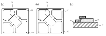
도 2a 내지 도 2b는 본 발명의 다른 실시예에 따른 홀 센서의 제조방법을 설명하기 위한 모식도이다.
도 3은 본 발명의 일 실시예에 따른 홀 센서를 모식화한 측면도이다.
도 4는 종래의 홀 센서의 구조를 나타낸 모식도이다.
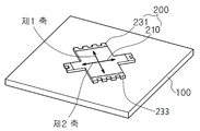
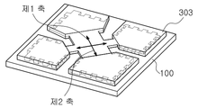
210, 220: 활성층의 감지부 230, 240: 활성층의 요철 패턴부
231, 241: 제1 접촉부 233, 243: 제2 접촉부
301, 303: 전극부 310: 오믹금속층
330: 금속배선층
Claims (15)
- 반도체 기판 상에 배치된, 제1 축 및 제2 축이 수직으로 교차된 십자 형태의 감지부 및 상기 감지부와 일체로 형성되며 상기 감지부의 4개의 끝단에 연결하여 위치하는 요철 패턴부를 포함하는 활성층; 및
상기 요철 패턴부의 표면 및 상기 반도체 기판 상에 배치된 전극부를 포함하고,
상기 전극부는 상기 제1 축 방향의 요철 패턴부의 끝단에 서로 대향하여 위치하는 제1 금속층 및 제2 금속층과, 상기 제2 축의 방향의 요철 패턴부의 끝단에 서로 대향하여 위치하는 제3 금속층 및 제4 금속층으로 이루어지며,
상기 요철 패턴부 형상의 적어도 하나의 변은 복수의 오목부와 복수의 볼록부가 교대로 배열된 요철 구조를 포함하는 것을 특징으로 하는 홀 센서. - 제1항에 있어서,
상기 활성층은 n형 불순물로 도핑된 화합물 반도체를 포함하는 것을 특징으로 하는 홀 센서. - 제1항에 있어서, 상기 요철 패턴부는
상기 제1 축 방향으로 신장된 제1 요철 패턴부; 및
상기 제2 축 방향으로 신장된 제2 요철 패턴부를 포함하는 것을 특징으로 하는 홀 센서. - 제3항에 있어서,
상기 제1 요철 패턴부의 폭은 상기 감지부의 상기 제1 축 방향으로 신장된 부분의 폭과 동일한 것을 특징으로 하는 홀 센서. - 제3항에 있어서,
상기 제2 요철 패턴부의 폭은 상기 감지부의 상기 제2 축 방향으로 신장된 부분의 폭과 동일한 것을 특징으로 하는 홀 센서. - 제3항에 있어서,
상기 제 1 요철 패턴부는 상기 감지부로부터 상기 전극부의 형상을 따라 신장되어 상기 제1 요철 패턴부의 최대폭은 상기 감지부의 상기 제1 축 방향으로 신장된 부분의 최대폭보다 큰 것을 특징으로 하는 홀 센서. - 제3항에 있어서,
상기 제 2 요철 패턴부는 상기 감지부로부터 상기 전극부의 형상을 따라 신장되어 상기 제2 요철 패턴부의 최대폭은 상기 감지부의 상기 제2 축 방향으로 신장된 부분의 최대폭보다 큰 것을 특징으로 하는 홀 센서. - 제3항에 있어서,
상기 제1 요철 패턴부의 표면 및 상기 반도체 기판 상에 배치되는 상기 제1 금속층 및 상기 제2 금속층은 상기 홀 센서의 전원을 공급하는 전원입력 전극으로 사용되고,
상기 제2 요철 패턴부의 표면 및 상기 반도체 기판 상에 배치되는 상기 제3 금속층 및 상기 제4 금속층은 상기 홀 센서에서 생성된 홀 전압을 측정하는 홀 전압출력 전극으로 사용되는 것을 특징으로 하는 홀 센서. - 제1항에 있어서,
각각의 상기 제1 금속층 내지 상기 제 4금속층은,
상기 요철 패턴부의 표면 및 상기 반도체 기판 상에 배치된 오믹(ohmic)금속층; 및
상기 오믹금속층 상부에 배치된 금속배선층이 순차적으로 적층된 구조를 갖는 것을 특징으로 하는 홀 센서. - 제1항에 있어서,
상기 전극부 형상의 적어도 하나의 변은 상기 반도체 기판의 외주면을 따라 형성된 것을 특징으로 하는 홀 센서. - 반도체 기판 상에 박막 형태의 활성층을 형성하는 단계;
상기 활성층을, 제1 축 및 제2 축이 수직으로 교차된 십자형태의 감지부 및 상기 감지부와 일체로 형성되며 상기 감지부의 4개의 끝단에 위치되는 요철 패턴부를 포함하는 구조를 갖도록 식각하는 단계; 및
상기 요철 패턴부의 표면 및 상기 반도체 기판 상에 전극부를 형성하는 단계를 포함하며,
상기 전극부는, 상기 제1 축 방향의 요철 패턴부의 끝단에 서로 대향하여 위치하는 제1 금속층 및 제2 금속층과, 상기 제2 축 방향의 요철 패턴부의 끝단에 서로 대향하여 위치하는 제3 금속층 및 제4 금속층으로 이루어진 것이며,
상기 요철 패턴부 형상의 적어도 하나의 변은 복수의 오목부와 복수의 볼록부가 교대로 배열된 요철 구조를 포함하는 것을 특징으로 하는 홀 센서의 제조방법. - 제11항에 있어서,
이온 주입법을 이용하여 상기 활성층을 n형 불순물로 도핑시키는 단계를 더 포함하는 것을 특징으로 하는 홀 센서의 제조방법. - 제11항에 있어서,
상기 활성층을 식각하는 단계는, 습식식각, 건식식각, 또는 습식식각과 건식식각을 혼용하여 수행하는 것을 특징으로 하는 홀 센서의 제조방법. - 제11항에 있어서,
각각의 상기 제1 금속층 내지 상기 제 4금속층은,
상기 요철 패턴부의 표면 및 상기 반도체 기판 상에 배치된 오믹(ohmic)금속층; 및
상기 오믹금속층 상부에 배치된 금속배선층을 순차적으로 적층시켜 형성하는 것을 특징으로 하는 홀 센서의 제조방법. - 제11항에 있어서,
상기 전극부를 형성하는 단계는,
금속 리프트 오프(lift off) 공정 또는 금속 도금 공정을 이용하여 수행하는 것을 특징으로 하는 홀 센서의 제조방법.
Priority Applications (1)
| Application Number | Priority Date | Filing Date | Title |
|---|---|---|---|
| KR1020160019243A KR20170097828A (ko) | 2016-02-18 | 2016-02-18 | 요철 패턴을 갖는 활성층을 포함하는 홀 센서 및 이의 제조방법 |
Applications Claiming Priority (1)
| Application Number | Priority Date | Filing Date | Title |
|---|---|---|---|
| KR1020160019243A KR20170097828A (ko) | 2016-02-18 | 2016-02-18 | 요철 패턴을 갖는 활성층을 포함하는 홀 센서 및 이의 제조방법 |
Publications (1)
| Publication Number | Publication Date |
|---|---|
| KR20170097828A true KR20170097828A (ko) | 2017-08-29 |
Family
ID=59760084
Family Applications (1)
| Application Number | Title | Priority Date | Filing Date |
|---|---|---|---|
| KR1020160019243A Ceased KR20170097828A (ko) | 2016-02-18 | 2016-02-18 | 요철 패턴을 갖는 활성층을 포함하는 홀 센서 및 이의 제조방법 |
Country Status (1)
| Country | Link |
|---|---|
| KR (1) | KR20170097828A (ko) |
Cited By (4)
| Publication number | Priority date | Publication date | Assignee | Title |
|---|---|---|---|---|
| WO2020180977A1 (en) * | 2019-03-04 | 2020-09-10 | University Of Maryland, College Park | Systems, devices, and methods for resistance metrology using graphene with superconducting components |
| KR20210069421A (ko) | 2019-12-03 | 2021-06-11 | 엘지전자 주식회사 | 식기 세척기 및 식기 세척기의 제어 방법 |
| KR20230106960A (ko) * | 2022-01-07 | 2023-07-14 | 한국과학기술원 | 금속과 실리콘 접합 구조를 적용한 자기장 센서 |
| US12142182B2 (en) | 2022-01-04 | 2024-11-12 | Samsung Display Co., Ltd. | Display device and driving method of display device |
-
2016
- 2016-02-18 KR KR1020160019243A patent/KR20170097828A/ko not_active Ceased
Cited By (6)
| Publication number | Priority date | Publication date | Assignee | Title |
|---|---|---|---|---|
| WO2020180977A1 (en) * | 2019-03-04 | 2020-09-10 | University Of Maryland, College Park | Systems, devices, and methods for resistance metrology using graphene with superconducting components |
| US11867775B2 (en) | 2019-03-04 | 2024-01-09 | Government Of The United States Of America | Systems, devices, and methods for resistance metrology using graphene with superconducting components |
| KR20210069421A (ko) | 2019-12-03 | 2021-06-11 | 엘지전자 주식회사 | 식기 세척기 및 식기 세척기의 제어 방법 |
| US12142182B2 (en) | 2022-01-04 | 2024-11-12 | Samsung Display Co., Ltd. | Display device and driving method of display device |
| KR20230106960A (ko) * | 2022-01-07 | 2023-07-14 | 한국과학기술원 | 금속과 실리콘 접합 구조를 적용한 자기장 센서 |
| US12416690B2 (en) | 2022-01-07 | 2025-09-16 | Korea Advanced Institute Of Science And Technology | Magnetic sensor using metal and silicon junction structure |
Similar Documents
| Publication | Publication Date | Title |
|---|---|---|
| KR100576872B1 (ko) | 정전기 방전 방지기능을 갖는 질화물 반도체 발광소자 | |
| US9136432B2 (en) | High efficiency light emitting diode | |
| US9000476B2 (en) | Optoelectronic component | |
| US9099614B2 (en) | Semiconductor light emitting element | |
| WO2007021069A1 (en) | Light emitting diode employing an array of nanorods and method of fabricating the same | |
| KR20170097828A (ko) | 요철 패턴을 갖는 활성층을 포함하는 홀 센서 및 이의 제조방법 | |
| JP3706458B2 (ja) | 半導体発光素子 | |
| CN111710729B (zh) | 齐纳二极管及其制造方法 | |
| CN113224153A (zh) | 高电子迁移率晶体管及其制作方法 | |
| JP6204131B2 (ja) | 発光素子及びその製造方法 | |
| KR20030036032A (ko) | 3 내지 5족 화합물 반도체 및 반도체 장치 | |
| US11715766B2 (en) | Stacked high barrier III-V power semiconductor diode | |
| US7435605B2 (en) | Method for fabricating a component having an electrical contact region | |
| KR101786207B1 (ko) | 접촉면적이 확장된 활성층을 포함하는 홀 센서 및 이의 제조방법 | |
| KR20050031720A (ko) | 질화물 반도체 발광 소자 및 그 제조 방법 | |
| US20150263229A1 (en) | Semiconductor light-emitting device and method of manufacturing the same | |
| CN221176251U (zh) | 发光二极管 | |
| KR20200016585A (ko) | 실리콘카바이드 파워반도체 및 그 제조방법 | |
| KR101067938B1 (ko) | 쇼트키 배리어 다이오드 및 그 제조 방법 | |
| TW201145610A (en) | Semiconductor diode and method for manufacturing a semiconductor diode | |
| JP2003133561A (ja) | 3−5族化合物半導体および半導体装置 | |
| JP4572430B2 (ja) | オーミック電極の形成方法 | |
| JP4110417B2 (ja) | 面発光型装置及びその製造方法 | |
| JP4066886B2 (ja) | ショットキ障壁を有する半導体素子及びその製造方法 | |
| JP2583793B2 (ja) | 半導体基板 |
Legal Events
| Date | Code | Title | Description |
|---|---|---|---|
| A201 | Request for examination | ||
| PA0109 | Patent application |
Patent event code: PA01091R01D Comment text: Patent Application Patent event date: 20160218 |
|
| PA0201 | Request for examination | ||
| E902 | Notification of reason for refusal | ||
| PE0902 | Notice of grounds for rejection |
Comment text: Notification of reason for refusal Patent event date: 20170322 Patent event code: PE09021S01D |
|
| PG1501 | Laying open of application | ||
| E601 | Decision to refuse application | ||
| PE0601 | Decision on rejection of patent |
Patent event date: 20180130 Comment text: Decision to Refuse Application Patent event code: PE06012S01D Patent event date: 20170322 Comment text: Notification of reason for refusal Patent event code: PE06011S01I |