KR20170098367A - 지지 기판 및 이를 사용한 반도체 패키지의 제조방법 - Google Patents
지지 기판 및 이를 사용한 반도체 패키지의 제조방법 Download PDFInfo
- Publication number
- KR20170098367A KR20170098367A KR1020160019771A KR20160019771A KR20170098367A KR 20170098367 A KR20170098367 A KR 20170098367A KR 1020160019771 A KR1020160019771 A KR 1020160019771A KR 20160019771 A KR20160019771 A KR 20160019771A KR 20170098367 A KR20170098367 A KR 20170098367A
- Authority
- KR
- South Korea
- Prior art keywords
- plate
- inorganic material
- material layer
- thermal expansion
- expansion coefficient
- Prior art date
- Legal status (The legal status is an assumption and is not a legal conclusion. Google has not performed a legal analysis and makes no representation as to the accuracy of the status listed.)
- Granted
Links
Images









Classifications
-
- H—ELECTRICITY
- H10—SEMICONDUCTOR DEVICES; ELECTRIC SOLID-STATE DEVICES NOT OTHERWISE PROVIDED FOR
- H10W—GENERIC PACKAGES, INTERCONNECTIONS, CONNECTORS OR OTHER CONSTRUCTIONAL DETAILS OF DEVICES COVERED BY CLASS H10
- H10W74/00—Encapsulations, e.g. protective coatings
- H10W74/01—Manufacture or treatment
- H10W74/019—Manufacture or treatment using temporary auxiliary substrates
-
- H01L23/3735—
-
- B—PERFORMING OPERATIONS; TRANSPORTING
- B32—LAYERED PRODUCTS
- B32B—LAYERED PRODUCTS, i.e. PRODUCTS BUILT-UP OF STRATA OF FLAT OR NON-FLAT, e.g. CELLULAR OR HONEYCOMB, FORM
- B32B17/00—Layered products essentially comprising sheet glass, or glass, slag, or like fibres
- B32B17/06—Layered products essentially comprising sheet glass, or glass, slag, or like fibres comprising glass as the main or only constituent of a layer, next to another layer of a specific material
- B32B17/10—Layered products essentially comprising sheet glass, or glass, slag, or like fibres comprising glass as the main or only constituent of a layer, next to another layer of a specific material of synthetic resin
-
- H01L21/471—
-
- H01L23/142—
-
- H01L23/147—
-
- H01L23/3121—
-
- H01L23/3675—
-
- H01L23/4926—
-
- H01L23/4985—
-
- H—ELECTRICITY
- H10—SEMICONDUCTOR DEVICES; ELECTRIC SOLID-STATE DEVICES NOT OTHERWISE PROVIDED FOR
- H10P—GENERIC PROCESSES OR APPARATUS FOR THE MANUFACTURE OR TREATMENT OF DEVICES COVERED BY CLASS H10
- H10P72/00—Handling or holding of wafers, substrates or devices during manufacture or treatment thereof
- H10P72/70—Handling or holding of wafers, substrates or devices during manufacture or treatment thereof for supporting or gripping
- H10P72/74—Handling or holding of wafers, substrates or devices during manufacture or treatment thereof for supporting or gripping using temporarily an auxiliary support
-
- H—ELECTRICITY
- H10—SEMICONDUCTOR DEVICES; ELECTRIC SOLID-STATE DEVICES NOT OTHERWISE PROVIDED FOR
- H10W—GENERIC PACKAGES, INTERCONNECTIONS, CONNECTORS OR OTHER CONSTRUCTIONAL DETAILS OF DEVICES COVERED BY CLASS H10
- H10W72/00—Interconnections or connectors in packages
- H10W72/01—Manufacture or treatment
- H10W72/0198—Manufacture or treatment batch processes
-
- H—ELECTRICITY
- H10—SEMICONDUCTOR DEVICES; ELECTRIC SOLID-STATE DEVICES NOT OTHERWISE PROVIDED FOR
- H10P—GENERIC PROCESSES OR APPARATUS FOR THE MANUFACTURE OR TREATMENT OF DEVICES COVERED BY CLASS H10
- H10P72/00—Handling or holding of wafers, substrates or devices during manufacture or treatment thereof
- H10P72/70—Handling or holding of wafers, substrates or devices during manufacture or treatment thereof for supporting or gripping
- H10P72/74—Handling or holding of wafers, substrates or devices during manufacture or treatment thereof for supporting or gripping using temporarily an auxiliary support
- H10P72/7412—Handling or holding of wafers, substrates or devices during manufacture or treatment thereof for supporting or gripping using temporarily an auxiliary support the auxiliary support including means facilitating the separation of a device or wafer from the auxiliary support
-
- H—ELECTRICITY
- H10—SEMICONDUCTOR DEVICES; ELECTRIC SOLID-STATE DEVICES NOT OTHERWISE PROVIDED FOR
- H10P—GENERIC PROCESSES OR APPARATUS FOR THE MANUFACTURE OR TREATMENT OF DEVICES COVERED BY CLASS H10
- H10P72/00—Handling or holding of wafers, substrates or devices during manufacture or treatment thereof
- H10P72/70—Handling or holding of wafers, substrates or devices during manufacture or treatment thereof for supporting or gripping
- H10P72/74—Handling or holding of wafers, substrates or devices during manufacture or treatment thereof for supporting or gripping using temporarily an auxiliary support
- H10P72/7424—Handling or holding of wafers, substrates or devices during manufacture or treatment thereof for supporting or gripping using temporarily an auxiliary support used as a support during the manufacture of self-supporting substrates
-
- H—ELECTRICITY
- H10—SEMICONDUCTOR DEVICES; ELECTRIC SOLID-STATE DEVICES NOT OTHERWISE PROVIDED FOR
- H10P—GENERIC PROCESSES OR APPARATUS FOR THE MANUFACTURE OR TREATMENT OF DEVICES COVERED BY CLASS H10
- H10P72/00—Handling or holding of wafers, substrates or devices during manufacture or treatment thereof
- H10P72/70—Handling or holding of wafers, substrates or devices during manufacture or treatment thereof for supporting or gripping
- H10P72/74—Handling or holding of wafers, substrates or devices during manufacture or treatment thereof for supporting or gripping using temporarily an auxiliary support
- H10P72/744—Details of chemical or physical process used for separating the auxiliary support from a device or a wafer
- H10P72/7442—Separation by peeling
-
- H—ELECTRICITY
- H10—SEMICONDUCTOR DEVICES; ELECTRIC SOLID-STATE DEVICES NOT OTHERWISE PROVIDED FOR
- H10W—GENERIC PACKAGES, INTERCONNECTIONS, CONNECTORS OR OTHER CONSTRUCTIONAL DETAILS OF DEVICES COVERED BY CLASS H10
- H10W40/00—Arrangements for thermal protection or thermal control
- H10W40/20—Arrangements for cooling
- H10W40/25—Arrangements for cooling characterised by their materials
-
- H—ELECTRICITY
- H10—SEMICONDUCTOR DEVICES; ELECTRIC SOLID-STATE DEVICES NOT OTHERWISE PROVIDED FOR
- H10W—GENERIC PACKAGES, INTERCONNECTIONS, CONNECTORS OR OTHER CONSTRUCTIONAL DETAILS OF DEVICES COVERED BY CLASS H10
- H10W70/00—Package substrates; Interposers; Redistribution layers [RDL]
- H10W70/01—Manufacture or treatment
- H10W70/05—Manufacture or treatment of insulating or insulated package substrates, or of interposers, or of redistribution layers
- H10W70/08—Manufacture or treatment of insulating or insulated package substrates, or of interposers, or of redistribution layers by depositing layers on the chip or wafer, e.g. "chip-first" RDLs
- H10W70/09—Manufacture or treatment of insulating or insulated package substrates, or of interposers, or of redistribution layers by depositing layers on the chip or wafer, e.g. "chip-first" RDLs extending onto an encapsulation that laterally surrounds the chip or wafer, e.g. fan-out wafer level package [FOWLP] RDLs
-
- H—ELECTRICITY
- H10—SEMICONDUCTOR DEVICES; ELECTRIC SOLID-STATE DEVICES NOT OTHERWISE PROVIDED FOR
- H10W—GENERIC PACKAGES, INTERCONNECTIONS, CONNECTORS OR OTHER CONSTRUCTIONAL DETAILS OF DEVICES COVERED BY CLASS H10
- H10W70/00—Package substrates; Interposers; Redistribution layers [RDL]
- H10W70/60—Insulating or insulated package substrates; Interposers; Redistribution layers
-
- H—ELECTRICITY
- H10—SEMICONDUCTOR DEVICES; ELECTRIC SOLID-STATE DEVICES NOT OTHERWISE PROVIDED FOR
- H10W—GENERIC PACKAGES, INTERCONNECTIONS, CONNECTORS OR OTHER CONSTRUCTIONAL DETAILS OF DEVICES COVERED BY CLASS H10
- H10W72/00—Interconnections or connectors in packages
- H10W72/20—Bump connectors, e.g. solder bumps or copper pillars; Dummy bumps; Thermal bumps
- H10W72/241—Dispositions, e.g. layouts
-
- H—ELECTRICITY
- H10—SEMICONDUCTOR DEVICES; ELECTRIC SOLID-STATE DEVICES NOT OTHERWISE PROVIDED FOR
- H10W—GENERIC PACKAGES, INTERCONNECTIONS, CONNECTORS OR OTHER CONSTRUCTIONAL DETAILS OF DEVICES COVERED BY CLASS H10
- H10W72/00—Interconnections or connectors in packages
- H10W72/20—Bump connectors, e.g. solder bumps or copper pillars; Dummy bumps; Thermal bumps
- H10W72/241—Dispositions, e.g. layouts
- H10W72/244—Dispositions, e.g. layouts relative to underlying supporting features, e.g. bond pads, RDLs or vias
-
- H—ELECTRICITY
- H10—SEMICONDUCTOR DEVICES; ELECTRIC SOLID-STATE DEVICES NOT OTHERWISE PROVIDED FOR
- H10W—GENERIC PACKAGES, INTERCONNECTIONS, CONNECTORS OR OTHER CONSTRUCTIONAL DETAILS OF DEVICES COVERED BY CLASS H10
- H10W72/00—Interconnections or connectors in packages
- H10W72/90—Bond pads, in general
- H10W72/941—Dispositions of bond pads
- H10W72/9413—Dispositions of bond pads on encapsulations
-
- H—ELECTRICITY
- H10—SEMICONDUCTOR DEVICES; ELECTRIC SOLID-STATE DEVICES NOT OTHERWISE PROVIDED FOR
- H10W—GENERIC PACKAGES, INTERCONNECTIONS, CONNECTORS OR OTHER CONSTRUCTIONAL DETAILS OF DEVICES COVERED BY CLASS H10
- H10W74/00—Encapsulations, e.g. protective coatings
- H10W74/01—Manufacture or treatment
- H10W74/014—Manufacture or treatment using batch processing
-
- H—ELECTRICITY
- H10—SEMICONDUCTOR DEVICES; ELECTRIC SOLID-STATE DEVICES NOT OTHERWISE PROVIDED FOR
- H10W—GENERIC PACKAGES, INTERCONNECTIONS, CONNECTORS OR OTHER CONSTRUCTIONAL DETAILS OF DEVICES COVERED BY CLASS H10
- H10W74/00—Encapsulations, e.g. protective coatings
- H10W74/10—Encapsulations, e.g. protective coatings characterised by their shape or disposition
- H10W74/111—Encapsulations, e.g. protective coatings characterised by their shape or disposition the semiconductor body being completely enclosed
- H10W74/114—Encapsulations, e.g. protective coatings characterised by their shape or disposition the semiconductor body being completely enclosed by a substrate and the encapsulations
- H10W74/117—Encapsulations, e.g. protective coatings characterised by their shape or disposition the semiconductor body being completely enclosed by a substrate and the encapsulations the substrate having spherical bumps for external connection
Landscapes
- Structures Or Materials For Encapsulating Or Coating Semiconductor Devices Or Solid State Devices (AREA)
- Engineering & Computer Science (AREA)
- Chemical & Material Sciences (AREA)
- Ceramic Engineering (AREA)
- Microelectronics & Electronic Packaging (AREA)
- Laminated Bodies (AREA)
Abstract
Description
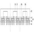
도 1은 실시예에 따른 반도체 패키지를 도시한 단면도이다.
도 2a 내지 도 2e는 실시예들에 따른 반도체 패키지의 제조 과정을 도시한 단면도이다.
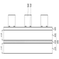
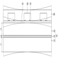
도 3a는 실시예들에 따른 지지 기판을 도시한 단면도이다.
도 3b는 도 3a의 지지 기판을 사용한 반도체 패키지의 제조의 일 단계을 도시한 것으로, 몰딩막의 경화 과정에 대응된다.
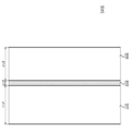
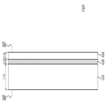
도 4a는 실시예들에 따른 지지 기판을 도시한 단면도이다.
도 4b는 도 4a의 지지 기판을 사용한 반도체 패키지의 제조에서 몰딩막의 경화 과정을 도시하였다.
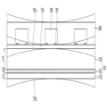
도 5a는 실시예들에 따른 지지 기판을 도시한 단면도이다.
도 5b는 도 5a의 지지 기판을 사용한 반도체 패키지의 제조에서 몰딩막의 경화 과정을 도시하였다.
도 6a는 실시예들에 따른 지지 기판을 도시한 단면도이다.
도 6b는 도 6a의 지지 기판을 사용한 반도체 패키지의 제조에서 몰딩막의 경화 과정을 도시하였다.
도 7a는 실시예들에 따른 지지 기판을 도시한 단면도이다.
도 7b는 도 7a의 지지 기판을 사용한 반도체 패키지의 제조에서 몰딩막의 경화 과정을 도시하였다.
Claims (19)
- 제1 플레이트;
상기 제1 플레이트 상의 제2 플레이트; 및
상기 제1 플레이트 및 상기 제2 플레이트 사이에 개재된 접착층을 포함하되,
상기 접착층은 상기 제1 플레이트 및 상기 제2 플레이트보다 높은 열팽창계수를 갖는 지지 기판. - 제1 항에 있어서,
상기 제1 플레이트는 상기 제2 플레이트보다 높은 열팽창계수를 가지며,
상기 제1 플레이트는 상기 제2 플레이트와 동일한 두께를 갖는 지지 기판. - 제1 항에 있어서,
상기 제1 플레이트는 상기 제2 플레이트보다 높은 열팽창계수를 가지며,
상기 제1 플레이트는 상기 제2 플레이트보다 더 얇은 두께를 갖는 지지 기판. - 제3 항에 있어서,
상기 제1 플레이트, 상기 접착층, 및 상기 제2 플레이트의 두께들의 합은 0.7mm 내지 1.5mm인 지지 기판. - 제1 항에 있어서,
상기 제1 플레이트는 상기 제2 플레이트보다 얇은 지지 기판. - 제5 항에 있어서,
상기 제1 플레이트는 상기 제2 플레이트와 동일한 열팽창계수를 가지는 지지 기판. - 제1 무기물층;
상기 제1 무기물층 상에 제공되는 폴리머층; 및
상기 폴리머층 상의 제2 무기물층을 포함하되,
상기 폴리머층은 상기 제1 무기물층 및 상기 제2 무기물층보다 높은 열 팽창계수를 갖는 지지 기판. - 제7 항에 있어서,
상기 제1 무기물층은 상기 제2 무기물층보다 높은 열팽창계수를 갖는 지지 기판. - 제8 항에 있어서,
상기 제1 무기물층은 상기 제2 무기물층과 다른 두께를 갖는 지지 기판. - 제7 항에 있어서,
상기 제1 무기물층은 상기 제2 무기물층과 동일한 두께를 갖는 지지 기판. - 제10 항에 있어서,
상기 제2 무기물층을 구성하는 원소들 중에서 적어도 하나는 상기 제1 무기물층을 구성하는 원소들과 다른 지지 기판. - 제10 항에 있어서,
상기 제2 무기물층을 구성하는 원소들은 상기 제1 무기물층을 구성하는 원소들과 동일하되, 상기 제2 무기물층의 조성비는 상기 제1 무기물층의 조성비와 다른 지지 기판. - 제12 항에 있어서,
제1 무기물층은 상기 제2 무기물층보다 얇은 두께를 가지되,
상기 제1 무기물층은 상기 제1 무기물층과 동일한 원소들을 포함하며, 상기 제1 무기물층의 조성비는 상기 제2 무기물층의 조성비와 동일한 지지 기판. - 적층된 제1 플레이트, 접착층, 및 제2 플레이트를 포함하는 지지 기판을 제공하는 것;
상기 지지 기판 상에 반도체칩을 배치하는 것;
상기 지지 기판 상에 상기 반도체칩을 덮는 몰딩막을 형성하는 것; 및
상기 지지 기판을 제거하여, 상기 반도체칩의 하면을 노출시키는 것을 포함하되,
상기 접착층은 상기 제1 플레이트 및 상기 제2 플레이트보다 높은 열팽창계수를 갖는 반도체 패키지 제조방법. - 제14 항에 있어서,
상기 제1 플레이트는 상기 제2 플레이트보다 높은 열팽창계수를 갖는 반도체 패키지 제조방법. - 제15 항에 있어서,
상기 지지 기판은 상기 반도체칩을 향하는 상면 및 상기 상면과 대향되는 하면을 가지고,
상기 접착층은 상기 지지 기판의 상기 상면보다 상기 하면에 더 인접하여 제공되는 반도체 패키지 제조방법. - 제14 항에 있어서,
상기 제1 플레이트는 상기 제2 플레이트와 동일한 두께를 갖는 반도체 패키지 제조방법. - 제14 항에 있어서,
상기 반도체칩의 상기 하면 상에 기판을 형성하는 것을 더 포함하되,
상기 기판은 절연 패턴들 및 상기 절연 패턴들 사이의 도전 패턴을 포함하는 반도체 패키지 제조방법. - 제14 항에 있어서,
상기 몰딩막을 형성하는 것은:
상기 지지 기판 상에 몰딩 물질을 공급하여, 상기 반도체칩을 덮는 것; 및
상기 몰딩 물질을 경화시키는 것을 포함하는 반도체 패키지 제조방법.
Priority Applications (3)
| Application Number | Priority Date | Filing Date | Title |
|---|---|---|---|
| KR1020160019771A KR102466362B1 (ko) | 2016-02-19 | 2016-02-19 | 지지 기판 및 이를 사용한 반도체 패키지의 제조방법 |
| US15/345,534 US9947554B2 (en) | 2016-02-19 | 2016-11-08 | Support substrate and a method of manufacturing a semiconductor package using the same |
| CN201710041269.8A CN107104070B (zh) | 2016-02-19 | 2017-01-20 | 支撑基底以及使用支撑基底制造半导体封装件的方法 |
Applications Claiming Priority (1)
| Application Number | Priority Date | Filing Date | Title |
|---|---|---|---|
| KR1020160019771A KR102466362B1 (ko) | 2016-02-19 | 2016-02-19 | 지지 기판 및 이를 사용한 반도체 패키지의 제조방법 |
Publications (2)
| Publication Number | Publication Date |
|---|---|
| KR20170098367A true KR20170098367A (ko) | 2017-08-30 |
| KR102466362B1 KR102466362B1 (ko) | 2022-11-15 |
Family
ID=59631178
Family Applications (1)
| Application Number | Title | Priority Date | Filing Date |
|---|---|---|---|
| KR1020160019771A Active KR102466362B1 (ko) | 2016-02-19 | 2016-02-19 | 지지 기판 및 이를 사용한 반도체 패키지의 제조방법 |
Country Status (3)
| Country | Link |
|---|---|
| US (1) | US9947554B2 (ko) |
| KR (1) | KR102466362B1 (ko) |
| CN (1) | CN107104070B (ko) |
Cited By (1)
| Publication number | Priority date | Publication date | Assignee | Title |
|---|---|---|---|---|
| KR20200046265A (ko) * | 2018-10-24 | 2020-05-07 | 삼성전자주식회사 | 캐리어 기판 및 이를 이용한 패키징 방법 |
Families Citing this family (7)
| Publication number | Priority date | Publication date | Assignee | Title |
|---|---|---|---|---|
| US11393701B2 (en) | 2019-08-12 | 2022-07-19 | Taiwan Semiconductor Manufacturing Company, Ltd. | Anisotropic carrier for high aspect ratio fanout |
| KR102767982B1 (ko) * | 2019-10-15 | 2025-02-14 | 에스케이하이닉스 주식회사 | 웨이퍼 지지 구조체 |
| CN111508902B (zh) * | 2020-04-26 | 2021-09-10 | 全球能源互联网研究院有限公司 | 一种绝缘结构、包覆芯片周缘的绝缘件及其制备方法 |
| TW202143401A (zh) * | 2020-05-08 | 2021-11-16 | 力成科技股份有限公司 | 半導體封裝方法及其結構 |
| CN113436979B (zh) * | 2021-06-15 | 2024-02-27 | 矽磐微电子(重庆)有限公司 | 半导体封装方法 |
| TWI769109B (zh) * | 2021-11-05 | 2022-06-21 | 友達光電股份有限公司 | 封裝結構及其製造方法 |
| CN116525551A (zh) * | 2022-01-24 | 2023-08-01 | 群创光电股份有限公司 | 电子元件的封装结构的制造方法 |
Citations (4)
| Publication number | Priority date | Publication date | Assignee | Title |
|---|---|---|---|---|
| US20090179317A1 (en) * | 2008-01-11 | 2009-07-16 | Kabushiki Kaisha Toshiba | Semiconductor device and method for manufacturing the same |
| US20100201462A1 (en) * | 2002-03-18 | 2010-08-12 | Qualcomm Incorporated | Flexible interconnect cable for an electronic assembly |
| US20140226290A1 (en) * | 2011-09-30 | 2014-08-14 | Kyocera Corporation | Wiring substrate, component embedded substrate, and package structure |
| US20160104620A1 (en) * | 2014-10-08 | 2016-04-14 | Toyota Jidosha Kabushiki Kaisha | Method for manufacturing substrate |
Family Cites Families (14)
| Publication number | Priority date | Publication date | Assignee | Title |
|---|---|---|---|---|
| US20030011108A1 (en) | 2001-07-12 | 2003-01-16 | Matthies Dennis L. | Assembly display modules |
| JP3888302B2 (ja) | 2002-12-24 | 2007-02-28 | カシオ計算機株式会社 | 半導体装置 |
| KR100906047B1 (ko) * | 2005-03-14 | 2009-07-03 | 스미토모 베이클리트 컴퍼니 리미티드 | 반도체 장치 |
| JP2007059821A (ja) * | 2005-08-26 | 2007-03-08 | Shinko Electric Ind Co Ltd | 配線基板の製造方法 |
| WO2008120705A1 (ja) * | 2007-03-29 | 2008-10-09 | Nec Corporation | 半導体装置 |
| KR100878408B1 (ko) | 2007-07-04 | 2009-01-13 | 삼성전기주식회사 | 웨이퍼 레벨 디바이스 패키징 방법 |
| JP5091696B2 (ja) | 2008-01-26 | 2012-12-05 | 株式会社フジクラ | 半導体パッケージの製造方法 |
| JP2011222946A (ja) * | 2010-03-26 | 2011-11-04 | Sumitomo Bakelite Co Ltd | 回路基板、半導体装置、回路基板の製造方法および半導体装置の製造方法 |
| US20140329083A1 (en) | 2010-04-06 | 2014-11-06 | Lg Hausys, Ltd. | Adhesive film for touch panel and touch panel |
| KR101156896B1 (ko) * | 2010-07-09 | 2012-06-21 | 삼성전기주식회사 | 반도체 패키지 기판 및 그 제조방법 |
| KR101679657B1 (ko) | 2010-09-29 | 2016-11-25 | 삼성전자주식회사 | 유리섬유를 이용한 웨이퍼 레벨 몰드 형성방법 및 그 방법에 의한 웨이퍼 구조 |
| KR101393701B1 (ko) | 2012-11-29 | 2014-05-13 | 서울과학기술대학교 산학협력단 | 웨이퍼의 휨 발생 방지와 방열기능을 부여하는 팬 아웃 웨이퍼 레벨 패키징 공정 |
| KR101393700B1 (ko) | 2012-11-29 | 2014-05-13 | 서울과학기술대학교 산학협력단 | 웨이퍼의 휨 발생 방지 기능을 강화시킨 팬 아웃 웨이퍼 레벨 패키징 공정 |
| KR101494814B1 (ko) | 2013-04-15 | 2015-02-23 | 앰코 테크놀로지 코리아 주식회사 | 팬 아웃 반도체 패키지 및 그 제조 방법 |
-
2016
- 2016-02-19 KR KR1020160019771A patent/KR102466362B1/ko active Active
- 2016-11-08 US US15/345,534 patent/US9947554B2/en active Active
-
2017
- 2017-01-20 CN CN201710041269.8A patent/CN107104070B/zh active Active
Patent Citations (4)
| Publication number | Priority date | Publication date | Assignee | Title |
|---|---|---|---|---|
| US20100201462A1 (en) * | 2002-03-18 | 2010-08-12 | Qualcomm Incorporated | Flexible interconnect cable for an electronic assembly |
| US20090179317A1 (en) * | 2008-01-11 | 2009-07-16 | Kabushiki Kaisha Toshiba | Semiconductor device and method for manufacturing the same |
| US20140226290A1 (en) * | 2011-09-30 | 2014-08-14 | Kyocera Corporation | Wiring substrate, component embedded substrate, and package structure |
| US20160104620A1 (en) * | 2014-10-08 | 2016-04-14 | Toyota Jidosha Kabushiki Kaisha | Method for manufacturing substrate |
Cited By (1)
| Publication number | Priority date | Publication date | Assignee | Title |
|---|---|---|---|---|
| KR20200046265A (ko) * | 2018-10-24 | 2020-05-07 | 삼성전자주식회사 | 캐리어 기판 및 이를 이용한 패키징 방법 |
Also Published As
| Publication number | Publication date |
|---|---|
| US20170243763A1 (en) | 2017-08-24 |
| US9947554B2 (en) | 2018-04-17 |
| KR102466362B1 (ko) | 2022-11-15 |
| CN107104070B (zh) | 2020-11-17 |
| CN107104070A (zh) | 2017-08-29 |
Similar Documents
| Publication | Publication Date | Title |
|---|---|---|
| KR102466362B1 (ko) | 지지 기판 및 이를 사용한 반도체 패키지의 제조방법 | |
| US7973398B2 (en) | Embedded chip package structure with chip support protruding section | |
| KR100907232B1 (ko) | 반도체 장치 및 그 제조 방법 | |
| TWI605528B (zh) | 包封晶粒、含有包封晶粒之微電子封裝體以及用於製造該微電子封裝體之方法(二) | |
| US9451700B2 (en) | Method for producing multi-layer substrate and multi-layer substrate | |
| CN102549785B (zh) | 发光装置 | |
| KR102180746B1 (ko) | 반도체 패키지 구조 및 그 제조 방법 | |
| US9799626B2 (en) | Semiconductor packages and other circuit modules with porous and non-porous stabilizing layers | |
| US10090276B2 (en) | Semiconductor package to reduce warping | |
| US7663248B2 (en) | Flip-chip component | |
| US11562969B2 (en) | Semiconductor device package including reinforced structure | |
| US7105920B2 (en) | Substrate design to improve chip package reliability | |
| KR100652442B1 (ko) | 반도체 칩 및 그 제조 방법 | |
| US7998834B2 (en) | Substrate level bonding method and substrate level package | |
| US20130119540A1 (en) | Semiconductor package and method for manufacturing the same | |
| CN113628981A (zh) | 半导体封装方法及其结构 | |
| TWI902086B (zh) | 扇出型封裝體的製備方法 | |
| US20250062185A1 (en) | Electronic package and manufacturing method thereof | |
| TWI819456B (zh) | 複合層電路元件及其製作方法 | |
| TWI875268B (zh) | 複合封裝基板 | |
| US20080191319A1 (en) | Semiconductor chip suppressing a void during a die attaching process and semiconductor package including the same | |
| Justin et al. | Evaluation of support wafer system for thin wafer handling | |
| KR100401148B1 (ko) | 반도체 패키지 제조용 부재 | |
| JP2006165275A (ja) | 半導体装置及びその製造方法 | |
| KR20260030277A (ko) | 반도체 장치용 캐리어 어셈블리 |
Legal Events
| Date | Code | Title | Description |
|---|---|---|---|
| PA0109 | Patent application |
St.27 status event code: A-0-1-A10-A12-nap-PA0109 |
|
| PG1501 | Laying open of application |
St.27 status event code: A-1-1-Q10-Q12-nap-PG1501 |
|
| A201 | Request for examination | ||
| E13-X000 | Pre-grant limitation requested |
St.27 status event code: A-2-3-E10-E13-lim-X000 |
|
| P11-X000 | Amendment of application requested |
St.27 status event code: A-2-2-P10-P11-nap-X000 |
|
| P13-X000 | Application amended |
St.27 status event code: A-2-2-P10-P13-nap-X000 |
|
| PA0201 | Request for examination |
St.27 status event code: A-1-2-D10-D11-exm-PA0201 |
|
| E902 | Notification of reason for refusal | ||
| PE0902 | Notice of grounds for rejection |
St.27 status event code: A-1-2-D10-D21-exm-PE0902 |
|
| P11-X000 | Amendment of application requested |
St.27 status event code: A-2-2-P10-P11-nap-X000 |
|
| P13-X000 | Application amended |
St.27 status event code: A-2-2-P10-P13-nap-X000 |
|
| E701 | Decision to grant or registration of patent right | ||
| PE0701 | Decision of registration |
St.27 status event code: A-1-2-D10-D22-exm-PE0701 |
|
| GRNT | Written decision to grant | ||
| PR0701 | Registration of establishment |
St.27 status event code: A-2-4-F10-F11-exm-PR0701 |
|
| PR1002 | Payment of registration fee |
St.27 status event code: A-2-2-U10-U11-oth-PR1002 Fee payment year number: 1 |
|
| PG1601 | Publication of registration |
St.27 status event code: A-4-4-Q10-Q13-nap-PG1601 |
|
| PR1001 | Payment of annual fee |
St.27 status event code: A-4-4-U10-U11-oth-PR1001 Fee payment year number: 4 |
|
| U11 | Full renewal or maintenance fee paid |
Free format text: ST27 STATUS EVENT CODE: A-4-4-U10-U11-OTH-PR1001 (AS PROVIDED BY THE NATIONAL OFFICE) Year of fee payment: 4 |
|
| P22-X000 | Classification modified |
St.27 status event code: A-4-4-P10-P22-nap-X000 |