KR20170101144A - 기능성 컨택터 및 이를 구비한 휴대용 전자장치 - Google Patents
기능성 컨택터 및 이를 구비한 휴대용 전자장치 Download PDFInfo
- Publication number
- KR20170101144A KR20170101144A KR1020170024466A KR20170024466A KR20170101144A KR 20170101144 A KR20170101144 A KR 20170101144A KR 1020170024466 A KR1020170024466 A KR 1020170024466A KR 20170024466 A KR20170024466 A KR 20170024466A KR 20170101144 A KR20170101144 A KR 20170101144A
- Authority
- KR
- South Korea
- Prior art keywords
- electrode
- conductor
- functional
- electronic device
- contactor
- Prior art date
- Legal status (The legal status is an assumption and is not a legal conclusion. Google has not performed a legal analysis and makes no representation as to the accuracy of the status listed.)
- Granted
Links
Images




Classifications
-
- H—ELECTRICITY
- H01—ELECTRIC ELEMENTS
- H01R—ELECTRICALLY-CONDUCTIVE CONNECTIONS; STRUCTURAL ASSOCIATIONS OF A PLURALITY OF MUTUALLY-INSULATED ELECTRICAL CONNECTING ELEMENTS; COUPLING DEVICES; CURRENT COLLECTORS
- H01R12/00—Structural associations of a plurality of mutually-insulated electrical connecting elements, specially adapted for printed circuits, e.g. printed circuit boards [PCB], flat or ribbon cables, or like generally planar structures, e.g. terminal strips, terminal blocks; Coupling devices specially adapted for printed circuits, flat or ribbon cables, or like generally planar structures; Terminals specially adapted for contact with, or insertion into, printed circuits, flat or ribbon cables, or like generally planar structures
- H01R12/70—Coupling devices
- H01R12/71—Coupling devices for rigid printing circuits or like structures
- H01R12/712—Coupling devices for rigid printing circuits or like structures co-operating with the surface of the printed circuit or with a coupling device exclusively provided on the surface of the printed circuit
- H01R12/716—Coupling device provided on the PCB
- H01R12/718—Contact members provided on the PCB without an insulating housing
-
- H—ELECTRICITY
- H01—ELECTRIC ELEMENTS
- H01R—ELECTRICALLY-CONDUCTIVE CONNECTIONS; STRUCTURAL ASSOCIATIONS OF A PLURALITY OF MUTUALLY-INSULATED ELECTRICAL CONNECTING ELEMENTS; COUPLING DEVICES; CURRENT COLLECTORS
- H01R13/00—Details of coupling devices of the kinds covered by groups H01R12/70 or H01R24/00 - H01R33/00
- H01R13/648—Protective earth or shield arrangements on coupling devices, e.g. anti-static shielding
- H01R13/6485—Electrostatic discharge protection
-
- H—ELECTRICITY
- H01—ELECTRIC ELEMENTS
- H01R—ELECTRICALLY-CONDUCTIVE CONNECTIONS; STRUCTURAL ASSOCIATIONS OF A PLURALITY OF MUTUALLY-INSULATED ELECTRICAL CONNECTING ELEMENTS; COUPLING DEVICES; CURRENT COLLECTORS
- H01R13/00—Details of coupling devices of the kinds covered by groups H01R12/70 or H01R24/00 - H01R33/00
- H01R13/02—Contact members
- H01R13/22—Contacts for co-operating by abutting
- H01R13/24—Contacts for co-operating by abutting resilient; resiliently-mounted
- H01R13/2407—Contacts for co-operating by abutting resilient; resiliently-mounted characterized by the resilient means
-
- H—ELECTRICITY
- H01—ELECTRIC ELEMENTS
- H01R—ELECTRICALLY-CONDUCTIVE CONNECTIONS; STRUCTURAL ASSOCIATIONS OF A PLURALITY OF MUTUALLY-INSULATED ELECTRICAL CONNECTING ELEMENTS; COUPLING DEVICES; CURRENT COLLECTORS
- H01R13/00—Details of coupling devices of the kinds covered by groups H01R12/70 or H01R24/00 - H01R33/00
- H01R13/02—Contact members
- H01R13/22—Contacts for co-operating by abutting
- H01R13/24—Contacts for co-operating by abutting resilient; resiliently-mounted
- H01R13/2407—Contacts for co-operating by abutting resilient; resiliently-mounted characterized by the resilient means
- H01R13/2428—Contacts for co-operating by abutting resilient; resiliently-mounted characterized by the resilient means using meander springs
-
- H—ELECTRICITY
- H01—ELECTRIC ELEMENTS
- H01R—ELECTRICALLY-CONDUCTIVE CONNECTIONS; STRUCTURAL ASSOCIATIONS OF A PLURALITY OF MUTUALLY-INSULATED ELECTRICAL CONNECTING ELEMENTS; COUPLING DEVICES; CURRENT COLLECTORS
- H01R13/00—Details of coupling devices of the kinds covered by groups H01R12/70 or H01R24/00 - H01R33/00
- H01R13/02—Contact members
- H01R13/22—Contacts for co-operating by abutting
- H01R13/24—Contacts for co-operating by abutting resilient; resiliently-mounted
- H01R13/2442—Contacts for co-operating by abutting resilient; resiliently-mounted with a single cantilevered beam
-
- H—ELECTRICITY
- H01—ELECTRIC ELEMENTS
- H01R—ELECTRICALLY-CONDUCTIVE CONNECTIONS; STRUCTURAL ASSOCIATIONS OF A PLURALITY OF MUTUALLY-INSULATED ELECTRICAL CONNECTING ELEMENTS; COUPLING DEVICES; CURRENT COLLECTORS
- H01R13/00—Details of coupling devices of the kinds covered by groups H01R12/70 or H01R24/00 - H01R33/00
- H01R13/66—Structural association with built-in electrical component
- H01R13/70—Structural association with built-in electrical component with built-in switch
- H01R13/703—Structural association with built-in electrical component with built-in switch operated by engagement or disengagement of coupling parts, e.g. dual-continuity coupling part
- H01R13/7031—Shorting, shunting or bussing of different terminals interrupted or effected on engagement of coupling part, e.g. for ESD protection, line continuity
-
- H—ELECTRICITY
- H05—ELECTRIC TECHNIQUES NOT OTHERWISE PROVIDED FOR
- H05K—PRINTED CIRCUITS; CASINGS OR CONSTRUCTIONAL DETAILS OF ELECTRIC APPARATUS; MANUFACTURE OF ASSEMBLAGES OF ELECTRICAL COMPONENTS
- H05K1/00—Printed circuits
- H05K1/02—Details
- H05K1/0213—Electrical arrangements not otherwise provided for
- H05K1/0254—High voltage adaptations; Electrical insulation details; Overvoltage or electrostatic discharge protection ; Arrangements for regulating voltages or for using plural voltages
- H05K1/0257—Overvoltage protection
- H05K1/0259—Electrostatic discharge [ESD] protection
-
- H—ELECTRICITY
- H05—ELECTRIC TECHNIQUES NOT OTHERWISE PROVIDED FOR
- H05K—PRINTED CIRCUITS; CASINGS OR CONSTRUCTIONAL DETAILS OF ELECTRIC APPARATUS; MANUFACTURE OF ASSEMBLAGES OF ELECTRICAL COMPONENTS
- H05K1/00—Printed circuits
- H05K1/02—Details
- H05K1/0266—Marks, test patterns or identification means
- H05K1/0268—Marks, test patterns or identification means for electrical inspection or testing
-
- H—ELECTRICITY
- H05—ELECTRIC TECHNIQUES NOT OTHERWISE PROVIDED FOR
- H05K—PRINTED CIRCUITS; CASINGS OR CONSTRUCTIONAL DETAILS OF ELECTRIC APPARATUS; MANUFACTURE OF ASSEMBLAGES OF ELECTRICAL COMPONENTS
- H05K1/00—Printed circuits
- H05K1/02—Details
- H05K1/03—Use of materials for the substrate
- H05K1/0306—Inorganic insulating substrates, e.g. ceramic, glass
-
- H—ELECTRICITY
- H05—ELECTRIC TECHNIQUES NOT OTHERWISE PROVIDED FOR
- H05K—PRINTED CIRCUITS; CASINGS OR CONSTRUCTIONAL DETAILS OF ELECTRIC APPARATUS; MANUFACTURE OF ASSEMBLAGES OF ELECTRICAL COMPONENTS
- H05K9/00—Screening of apparatus or components against electric or magnetic fields
- H05K9/0007—Casings
- H05K9/0009—Casings with provisions to reduce EMI leakage through the joining parts
-
- H—ELECTRICITY
- H05—ELECTRIC TECHNIQUES NOT OTHERWISE PROVIDED FOR
- H05K—PRINTED CIRCUITS; CASINGS OR CONSTRUCTIONAL DETAILS OF ELECTRIC APPARATUS; MANUFACTURE OF ASSEMBLAGES OF ELECTRICAL COMPONENTS
- H05K9/00—Screening of apparatus or components against electric or magnetic fields
- H05K9/0007—Casings
- H05K9/0015—Gaskets or seals
- H05K9/0016—Gaskets or seals having a spring contact
-
- H—ELECTRICITY
- H05—ELECTRIC TECHNIQUES NOT OTHERWISE PROVIDED FOR
- H05K—PRINTED CIRCUITS; CASINGS OR CONSTRUCTIONAL DETAILS OF ELECTRIC APPARATUS; MANUFACTURE OF ASSEMBLAGES OF ELECTRICAL COMPONENTS
- H05K9/00—Screening of apparatus or components against electric or magnetic fields
- H05K9/0067—Devices for protecting against damage from electrostatic discharge
-
- H—ELECTRICITY
- H05—ELECTRIC TECHNIQUES NOT OTHERWISE PROVIDED FOR
- H05K—PRINTED CIRCUITS; CASINGS OR CONSTRUCTIONAL DETAILS OF ELECTRIC APPARATUS; MANUFACTURE OF ASSEMBLAGES OF ELECTRICAL COMPONENTS
- H05K1/00—Printed circuits
- H05K1/02—Details
- H05K1/0213—Electrical arrangements not otherwise provided for
- H05K1/0215—Grounding of printed circuits by connection to external grounding means
-
- H—ELECTRICITY
- H05—ELECTRIC TECHNIQUES NOT OTHERWISE PROVIDED FOR
- H05K—PRINTED CIRCUITS; CASINGS OR CONSTRUCTIONAL DETAILS OF ELECTRIC APPARATUS; MANUFACTURE OF ASSEMBLAGES OF ELECTRICAL COMPONENTS
- H05K1/00—Printed circuits
- H05K1/02—Details
- H05K1/14—Structural association of two or more printed circuits
- H05K1/144—Stacked arrangements of planar printed circuit boards
-
- H—ELECTRICITY
- H05—ELECTRIC TECHNIQUES NOT OTHERWISE PROVIDED FOR
- H05K—PRINTED CIRCUITS; CASINGS OR CONSTRUCTIONAL DETAILS OF ELECTRIC APPARATUS; MANUFACTURE OF ASSEMBLAGES OF ELECTRICAL COMPONENTS
- H05K2201/00—Indexing scheme relating to printed circuits covered by H05K1/00
- H05K2201/01—Dielectrics
- H05K2201/0183—Dielectric layers
- H05K2201/0187—Dielectric layers with regions of different dielectrics in the same layer, e.g. in a printed capacitor for locally changing the dielectric properties
-
- H—ELECTRICITY
- H05—ELECTRIC TECHNIQUES NOT OTHERWISE PROVIDED FOR
- H05K—PRINTED CIRCUITS; CASINGS OR CONSTRUCTIONAL DETAILS OF ELECTRIC APPARATUS; MANUFACTURE OF ASSEMBLAGES OF ELECTRICAL COMPONENTS
- H05K2201/00—Indexing scheme relating to printed circuits covered by H05K1/00
- H05K2201/03—Conductive materials
- H05K2201/0302—Properties and characteristics in general
- H05K2201/0314—Elastomeric connector or conductor, e.g. rubber with metallic filler
-
- H—ELECTRICITY
- H05—ELECTRIC TECHNIQUES NOT OTHERWISE PROVIDED FOR
- H05K—PRINTED CIRCUITS; CASINGS OR CONSTRUCTIONAL DETAILS OF ELECTRIC APPARATUS; MANUFACTURE OF ASSEMBLAGES OF ELECTRICAL COMPONENTS
- H05K2201/00—Indexing scheme relating to printed circuits covered by H05K1/00
- H05K2201/04—Assemblies of printed circuits
- H05K2201/042—Stacked spaced PCBs; Planar parts of folded flexible circuits having mounted components in between or spaced from each other
-
- H—ELECTRICITY
- H05—ELECTRIC TECHNIQUES NOT OTHERWISE PROVIDED FOR
- H05K—PRINTED CIRCUITS; CASINGS OR CONSTRUCTIONAL DETAILS OF ELECTRIC APPARATUS; MANUFACTURE OF ASSEMBLAGES OF ELECTRICAL COMPONENTS
- H05K2201/00—Indexing scheme relating to printed circuits covered by H05K1/00
- H05K2201/10—Details of components or other objects attached to or integrated in a printed circuit board
- H05K2201/10227—Other objects, e.g. metallic pieces
- H05K2201/10265—Metallic coils or springs, e.g. as part of a connection element
-
- H—ELECTRICITY
- H05—ELECTRIC TECHNIQUES NOT OTHERWISE PROVIDED FOR
- H05K—PRINTED CIRCUITS; CASINGS OR CONSTRUCTIONAL DETAILS OF ELECTRIC APPARATUS; MANUFACTURE OF ASSEMBLAGES OF ELECTRICAL COMPONENTS
- H05K2201/00—Indexing scheme relating to printed circuits covered by H05K1/00
- H05K2201/10—Details of components or other objects attached to or integrated in a printed circuit board
- H05K2201/10227—Other objects, e.g. metallic pieces
- H05K2201/1031—Surface mounted metallic connector elements
-
- Y—GENERAL TAGGING OF NEW TECHNOLOGICAL DEVELOPMENTS; GENERAL TAGGING OF CROSS-SECTIONAL TECHNOLOGIES SPANNING OVER SEVERAL SECTIONS OF THE IPC; TECHNICAL SUBJECTS COVERED BY FORMER USPC CROSS-REFERENCE ART COLLECTIONS [XRACs] AND DIGESTS
- Y02—TECHNOLOGIES OR APPLICATIONS FOR MITIGATION OR ADAPTATION AGAINST CLIMATE CHANGE
- Y02P—CLIMATE CHANGE MITIGATION TECHNOLOGIES IN THE PRODUCTION OR PROCESSING OF GOODS
- Y02P70/00—Climate change mitigation technologies in the production process for final industrial or consumer products
- Y02P70/50—Manufacturing or production processes characterised by the final manufactured product
Landscapes
- Engineering & Computer Science (AREA)
- Microelectronics & Electronic Packaging (AREA)
- Chemical & Material Sciences (AREA)
- Ceramic Engineering (AREA)
- Inorganic Chemistry (AREA)
- Telephone Set Structure (AREA)
- Thermistors And Varistors (AREA)
- Measuring Leads Or Probes (AREA)
Abstract
Description
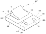
도 2는 본 발명의 일 실시예에 따른 기능성 컨택터의 일례의 사시도,
도 3은 본 발명의 일 실시예에 따른 기능성 컨택터의 다른 예의 사시도,
도 4는 본 발명의 일 실시예에 따른 기능성 컨택터에서 연결부가 캐스텔레이션 형태로 이루어진 경우의 단면도,
도 5는 도 4의 사시도,
도 6은 본 발명의 일 실시예에 따른 기능성 컨택터에서 연결부가 전극 형태로 이루어진 경우의 단면도,
도 7은 도 6의 사시도,
도 8은 본 발명의 일 실시예에 따른 기능성 컨택터에서 연결부가 양측에 구비된 경우의 단면도,
도 9는 본 발명의 일 실시예에 따른 기능성 컨택터에서 탄성을 갖는 전도체가 개스킷인 경우의 전극 형태로 이루어진 경우의 단면도,
도 10은 본 발명의 일 실시예에 따른 기능성 컨택터에서 기능소자의 일례를 나타낸 단면도, 그리고,
도 11은 본 발명의 일 실시예에 따른 기능성 컨택터에서 기능소자의 다른 예를 나타낸 단면도이다.
14a: 수용부 15 : 도전성 접착층
100,100a,100b,100c,200 : 컨택터
110 : 탄성을 갖는 전도체 110a : 도전성 접착층 또는 솔더
120 : 기능소자 120a : 몸체
121 : 제1전극 122 : 제2전극
123a,123a' : 제1검사용전극 123b : 제2검사용전극
123c,123d : 연장부 124 : 관통전극
124a,124b,124b' : 연결부 125a,125b : 내부전극
126a,126b: 중간전극 127 : 공극
128a,128b : 커패시터전극
Claims (15)
- 전자장치의 전도체에 전기적으로 접촉되는 탄성을 갖는 전도체;
상기 탄성을 갖는 전도체에 연결되며, 하면 및 상면의 적어도 일부에 각각 제1전극 및 제2전극이 구비되는 기능소자;
상기 제1전극에 연결되며 상기 기능소자의 상면에서 상기 제2전극과 일정 거리 이격되어 구비되는 제1검사용전극; 및
상기 제2전극에 연결되며 상기 기능소자의 상면에 구비되는 제2검사용전극을 포함하는 기능성 컨택터. - 제1항에 있어서,
상기 기능소자를 수직 관통하여 상기 제1검사용전극과 상기 제1전극을 연결하는 비아홀; 및 상기 비아홀에 충진된 도전성 물질을 더 포함하는 기능성 컨택터. - 제1항에 있어서,
상기 기능소자의 측면의 적어도 일부에 구비되어 상기 제1검사용전극과 상기 제1전극을 연결하는 연결부를 더 포함하는 기능성 컨택터. - 제3항에 있어서,
상기 연결부는 캐스텔레이션(castellation) 형태로 구비되거나 전극 형태로 구비되는 기능성 컨택터. - 제3항에 있어서,
상기 연결부는 상기 제1검사용전극과 일체로 이루어지는 기능성 컨택터. - 제5항에 있어서,
상기 전극 형태의 연결부는 상기 기능소자의 양측면 전체에 구비되고,
상기 제1검사용전극은 상기 기능소자의 상면에서 상기 제2전극의 양측에 대칭으로 구비되는 기능성 컨택터. - 제1항에 있어서,
상기 제2검사용전극은 상기 제2전극의 적어도 일부인 기능성 컨택터. - 제1항에 있어서,
상기 탄성을 갖는 전도체는 도전성 접착층 또는 솔더를 통하여 상기 제2전극 상에 적층되는 기능성 컨택터. - 제1항에 있어서,
상기 기능소자는 상기 전자장치의 전도체의 수용부에 도전성 접착층을 통하여 결합되는 기능성 컨택터. - 제1항에 있어서,
상기 탄성을 갖는 전도체는 도전성 개스킷, 실리콘 고무 패드, 및 C-클립 중 어느 하나인 기능성 컨택터. - 제1항에 있어서,
상기 기능소자는 상기 전자장치의 회로기판의 접지로부터 유입되는 외부전원의 누설전류를 차단하는 감전 방지 기능, 상기 전자장치의 전도체 또는 상기 회로기판으로부터 유입되는 통신 신호를 통과시키는 통신 신호 전달 기능, 및 상기 전자장치의 전도체로부터 정전기 유입시 방전에 의해 통과시키는 ESD 방호 기능 중 적어도 하나의 기능을 갖는 기능성 컨택터. - 인체 접촉가능한 외장 전도체;
내부 전도체; 및
상기 외장 전도체 및 상기 내부 전도체 중 어느 하나에 결합되며, 상기 외장 전도체와 상기 내부 전도체 사이에 직렬 연결되는 청구항 제1항 내지 제11항 중 어느 한 항에 기재된 기능성 컨택터를 포함하는 휴대용 전자장치. - 제12항에 있어서,
상기 외장 전도체 및 상기 내부 전도체 중 상기 기능성 컨택터가 결합되는 전도체는 상기 기능성 컨택터를 수용하기 위한 수용부가 구비되는 휴대용 전자장치. - 제12항에 있어서,
상기 외장 전도체는 상기 전자장치와 외부기기의 통신을 위한 안테나, 메탈 케이스, 및 도전성 장신구 중 어느 하나인 휴대용 전자장치. - 제12항에 있어서,
상기 내부 전도체는 도전성 브래킷 또는 회로기판인 휴대용 전자장치.
Priority Applications (2)
| Application Number | Priority Date | Filing Date | Title |
|---|---|---|---|
| US16/079,834 US10756472B2 (en) | 2016-02-26 | 2017-02-24 | Functional contactor and portable electronic device comprising same |
| PCT/KR2017/002051 WO2017146517A1 (ko) | 2016-02-26 | 2017-02-24 | 기능성 컨택터 및 이를 구비한 휴대용 전자장치 |
Applications Claiming Priority (2)
| Application Number | Priority Date | Filing Date | Title |
|---|---|---|---|
| KR1020160023567 | 2016-02-26 | ||
| KR20160023567 | 2016-02-26 |
Publications (2)
| Publication Number | Publication Date |
|---|---|
| KR20170101144A true KR20170101144A (ko) | 2017-09-05 |
| KR101887369B1 KR101887369B1 (ko) | 2018-09-06 |
Family
ID=59924969
Family Applications (1)
| Application Number | Title | Priority Date | Filing Date |
|---|---|---|---|
| KR1020170024466A Active KR101887369B1 (ko) | 2016-02-26 | 2017-02-24 | 기능성 컨택터 및 이를 구비한 휴대용 전자장치 |
Country Status (3)
| Country | Link |
|---|---|
| US (1) | US10756472B2 (ko) |
| KR (1) | KR101887369B1 (ko) |
| CN (1) | CN108701943B (ko) |
Cited By (2)
| Publication number | Priority date | Publication date | Assignee | Title |
|---|---|---|---|---|
| WO2020009316A1 (ko) * | 2018-07-05 | 2020-01-09 | 삼성전자 주식회사 | 서지 전압으로부터 부품들을 보호하기 위한 전자 장치 및 그에 관한 구조 |
| KR20210154792A (ko) * | 2020-06-05 | 2021-12-21 | 주식회사 나노엑스 | 반도체 소자 검사용 프로브 헤드 |
Families Citing this family (3)
| Publication number | Priority date | Publication date | Assignee | Title |
|---|---|---|---|---|
| KR101977270B1 (ko) * | 2016-02-24 | 2019-05-10 | 주식회사 아모텍 | 가이드 결합형 컨택터 및 이를 구비한 휴대용 전자장치 |
| EP3905861A1 (de) * | 2020-04-30 | 2021-11-03 | ZKW Group GmbH | Barriere gegen verschwimmen von smt-bauteilen |
| CN117063372A (zh) * | 2021-03-18 | 2023-11-14 | 三星电子株式会社 | 包括用于无线充电的天线构件的电子装置 |
Citations (6)
| Publication number | Priority date | Publication date | Assignee | Title |
|---|---|---|---|---|
| KR20070109332A (ko) | 2006-05-10 | 2007-11-15 | 삼성전기주식회사 | 무선통신 단말기의 내장 안테나 조립체 |
| KR20130026735A (ko) * | 2011-09-06 | 2013-03-14 | 삼성전자주식회사 | 인쇄회로 기판용 접촉 단자 |
| KR101339166B1 (ko) * | 2012-06-18 | 2013-12-09 | 주식회사 아이에스시 | 관통공이 형성된 도전성 입자를 가지는 검사용 소켓 및 그 제조방법 |
| KR101556936B1 (ko) * | 2014-08-25 | 2015-10-19 | 협진커넥터(주) | 표면 실장형 접속단자 |
| KR101585604B1 (ko) * | 2015-07-01 | 2016-01-14 | 주식회사 아모텍 | 감전보호용 컨택터 및 이를 구비한 휴대용 전자장치 |
| US9240645B1 (en) * | 2014-09-22 | 2016-01-19 | Foxconn Interconnect Technology Limited | Electrical contact |
Family Cites Families (20)
| Publication number | Priority date | Publication date | Assignee | Title |
|---|---|---|---|---|
| JP2793728B2 (ja) | 1991-09-26 | 1998-09-03 | 富士通株式会社 | シリアル/パラレル変換回路 |
| JPH11326379A (ja) | 1998-03-12 | 1999-11-26 | Fujitsu Ltd | 電子部品用コンタクタ及びその製造方法及びコンタクタ製造装置 |
| TW433591U (en) | 2000-02-02 | 2001-05-01 | Hon Hai Prec Ind Co Ltd | Electrical connector |
| JP4598779B2 (ja) * | 2004-11-16 | 2010-12-15 | 富士通セミコンダクター株式会社 | コンタクタ及びコンタクタを用いた試験方法 |
| KR100753187B1 (ko) | 2005-11-28 | 2007-08-30 | 엠텍비젼 주식회사 | 휴대 단말기 외부로 노출되는 칩 패키지 |
| KR100846343B1 (ko) * | 2006-10-27 | 2008-07-15 | 삼성전자주식회사 | 휴대용 무선단말기의 내장형 안테나 장치 |
| KR101472172B1 (ko) | 2007-09-26 | 2014-12-12 | 몰렉스 인코포레이티드 | 전기 부품 장착 조립체 |
| WO2009069270A1 (ja) * | 2007-11-27 | 2009-06-04 | Panasonic Corporation | 静電気対策部品およびその製造方法 |
| KR101033990B1 (ko) | 2010-09-03 | 2011-05-11 | 테크원 주식회사 | 카본알루미늄 복합소재를 이용한 파워 발광다이오드형 조명기구 |
| KR101915961B1 (ko) * | 2011-09-06 | 2019-01-31 | 삼성전자주식회사 | 전자 장치 및 그 전자 장치에 사용 가능한 보드 |
| KR102026695B1 (ko) | 2012-11-27 | 2019-09-30 | 엘지전자 주식회사 | 이동 단말기 |
| KR101638053B1 (ko) | 2015-09-18 | 2016-07-20 | 주식회사 아모텍 | 컨택터 및 이를 구비한 휴대용 전자장치 |
| WO2017146435A1 (ko) | 2016-02-24 | 2017-08-31 | 주식회사 아모텍 | 가이드 결합형 컨택터 및 이를 구비한 휴대용 전자장치 |
| KR101947425B1 (ko) | 2016-05-12 | 2019-02-13 | 주식회사 아모텍 | 기능성 컨택터 |
| KR101738984B1 (ko) * | 2016-05-26 | 2017-05-24 | 주식회사 모다이노칩 | 보호 컨택터 |
| CN109891680B (zh) | 2016-11-04 | 2021-11-16 | 阿莫技术有限公司 | 功能性接触器 |
| KR102565034B1 (ko) * | 2016-11-09 | 2023-08-09 | 주식회사 아모텍 | 기능성 컨택터 |
| US11165182B2 (en) * | 2016-12-21 | 2021-11-02 | Amotech Co., Ltd. | Functional contactor |
| US20190207386A1 (en) * | 2018-01-04 | 2019-07-04 | Ceramate Technical Co., Ltd. | Surge protection device structure |
| MX2020008622A (es) * | 2018-03-05 | 2021-01-15 | Kyocera Avx Components Corp | Varistor en cascada con mejores capacidades de manejo de energia. |
-
2017
- 2017-02-24 CN CN201780013576.3A patent/CN108701943B/zh active Active
- 2017-02-24 KR KR1020170024466A patent/KR101887369B1/ko active Active
- 2017-02-24 US US16/079,834 patent/US10756472B2/en active Active
Patent Citations (6)
| Publication number | Priority date | Publication date | Assignee | Title |
|---|---|---|---|---|
| KR20070109332A (ko) | 2006-05-10 | 2007-11-15 | 삼성전기주식회사 | 무선통신 단말기의 내장 안테나 조립체 |
| KR20130026735A (ko) * | 2011-09-06 | 2013-03-14 | 삼성전자주식회사 | 인쇄회로 기판용 접촉 단자 |
| KR101339166B1 (ko) * | 2012-06-18 | 2013-12-09 | 주식회사 아이에스시 | 관통공이 형성된 도전성 입자를 가지는 검사용 소켓 및 그 제조방법 |
| KR101556936B1 (ko) * | 2014-08-25 | 2015-10-19 | 협진커넥터(주) | 표면 실장형 접속단자 |
| US9240645B1 (en) * | 2014-09-22 | 2016-01-19 | Foxconn Interconnect Technology Limited | Electrical contact |
| KR101585604B1 (ko) * | 2015-07-01 | 2016-01-14 | 주식회사 아모텍 | 감전보호용 컨택터 및 이를 구비한 휴대용 전자장치 |
Cited By (3)
| Publication number | Priority date | Publication date | Assignee | Title |
|---|---|---|---|---|
| WO2020009316A1 (ko) * | 2018-07-05 | 2020-01-09 | 삼성전자 주식회사 | 서지 전압으로부터 부품들을 보호하기 위한 전자 장치 및 그에 관한 구조 |
| US11336762B2 (en) | 2018-07-05 | 2022-05-17 | Samsung Electronics Co., Ltd. | Electronic device for protecting components from surge voltage and structure thereof |
| KR20210154792A (ko) * | 2020-06-05 | 2021-12-21 | 주식회사 나노엑스 | 반도체 소자 검사용 프로브 헤드 |
Also Published As
| Publication number | Publication date |
|---|---|
| CN108701943A (zh) | 2018-10-23 |
| KR101887369B1 (ko) | 2018-09-06 |
| US10756472B2 (en) | 2020-08-25 |
| US20200212614A1 (en) | 2020-07-02 |
| CN108701943B (zh) | 2020-02-07 |
Similar Documents
| Publication | Publication Date | Title |
|---|---|---|
| KR101585604B1 (ko) | 감전보호용 컨택터 및 이를 구비한 휴대용 전자장치 | |
| KR101990415B1 (ko) | 가이드 결합형 컨택터 및 이를 구비한 휴대용 전자장치 | |
| KR101887369B1 (ko) | 기능성 컨택터 및 이를 구비한 휴대용 전자장치 | |
| CN109075483B (zh) | 功能性接触器 | |
| KR101939651B1 (ko) | 기능성 컨택터 및 이를 구비한 휴대용 전자장치 | |
| KR101638053B1 (ko) | 컨택터 및 이를 구비한 휴대용 전자장치 | |
| KR101959452B1 (ko) | 감전보호용 컨택터 결합체 및 이를 구비한 휴대용 전자장치 | |
| US20190281689A1 (en) | Functional contactor | |
| KR101969023B1 (ko) | 감전보호용 컨택터 결합체 및 이를 구비한 휴대용 전자장치 | |
| US10231366B2 (en) | Electric shock prevention apparatus | |
| KR101939658B1 (ko) | 감전보호용 컨택터 결합체 및 이를 구비한 휴대용 전자장치 | |
| KR101939649B1 (ko) | 감전보호용 컨택터 결합체 및 이를 구비한 휴대용 전자장치 | |
| KR20170048986A (ko) | 감전보호용 컨택터 및 이를 구비한 휴대용 전자장치 | |
| KR101916156B1 (ko) | 감전보호 장치 | |
| KR20170004797A (ko) | 감전보호용 컨택터 및 이를 구비한 휴대용 전자장치 | |
| KR20170053052A (ko) | 감전보호용 컨택터 및 이를 구비한 휴대용 전자장치 | |
| KR20170051068A (ko) | 감전보호용 컨택터 및 이를 구비한 휴대용 전자장치 | |
| KR20170053049A (ko) | 감전보호용 컨택터 및 이를 구비한 휴대용 전자장치 | |
| KR20170059780A (ko) | 감전보호용 컨택터 및 이를 구비한 휴대용 전자장치 | |
| KR20180051825A (ko) | 기능성 컨택터 및 이를 구비한 휴대용 전자장치 | |
| KR20170040639A (ko) | 감전보호용 컨택터 및 이를 구비한 휴대용 전자장치 | |
| KR20170048985A (ko) | 감전보호용 컨택터 및 이를 구비한 휴대용 전자장치 | |
| KR20170053053A (ko) | 감전보호용 컨택터 및 이를 구비한 휴대용 전자장치 |
Legal Events
| Date | Code | Title | Description |
|---|---|---|---|
| A201 | Request for examination | ||
| PA0109 | Patent application |
St.27 status event code: A-0-1-A10-A12-nap-PA0109 |
|
| PA0201 | Request for examination |
St.27 status event code: A-1-2-D10-D11-exm-PA0201 |
|
| PG1501 | Laying open of application |
St.27 status event code: A-1-1-Q10-Q12-nap-PG1501 |
|
| E902 | Notification of reason for refusal | ||
| PE0902 | Notice of grounds for rejection |
St.27 status event code: A-1-2-D10-D21-exm-PE0902 |
|
| P11-X000 | Amendment of application requested |
St.27 status event code: A-2-2-P10-P11-nap-X000 |
|
| P13-X000 | Application amended |
St.27 status event code: A-2-2-P10-P13-nap-X000 |
|
| E701 | Decision to grant or registration of patent right | ||
| PE0701 | Decision of registration |
St.27 status event code: A-1-2-D10-D22-exm-PE0701 |
|
| GRNT | Written decision to grant | ||
| PR0701 | Registration of establishment |
St.27 status event code: A-2-4-F10-F11-exm-PR0701 |
|
| PR1002 | Payment of registration fee |
St.27 status event code: A-2-2-U10-U11-oth-PR1002 Fee payment year number: 1 |
|
| PG1601 | Publication of registration |
St.27 status event code: A-4-4-Q10-Q13-nap-PG1601 |
|
| PR1001 | Payment of annual fee |
St.27 status event code: A-4-4-U10-U11-oth-PR1001 Fee payment year number: 4 |
|
| PR1001 | Payment of annual fee |
St.27 status event code: A-4-4-U10-U11-oth-PR1001 Fee payment year number: 5 |
|
| PR1001 | Payment of annual fee |
St.27 status event code: A-4-4-U10-U11-oth-PR1001 Fee payment year number: 6 |
|
| PN2301 | Change of applicant |
St.27 status event code: A-5-5-R10-R13-asn-PN2301 St.27 status event code: A-5-5-R10-R11-asn-PN2301 |
|
| PR1001 | Payment of annual fee |
St.27 status event code: A-4-4-U10-U11-oth-PR1001 Fee payment year number: 7 |
|
| PR1001 | Payment of annual fee |
St.27 status event code: A-4-4-U10-U11-oth-PR1001 Fee payment year number: 8 |
|
| U11 | Full renewal or maintenance fee paid |
Free format text: ST27 STATUS EVENT CODE: A-4-4-U10-U11-OTH-PR1001 (AS PROVIDED BY THE NATIONAL OFFICE) Year of fee payment: 8 |