KR20170101242A - 절연된 하부를 가지는 반도체 나노와이어 또는 마이크로와이어의 제조방법 - Google Patents
절연된 하부를 가지는 반도체 나노와이어 또는 마이크로와이어의 제조방법 Download PDFInfo
- Publication number
- KR20170101242A KR20170101242A KR1020177019191A KR20177019191A KR20170101242A KR 20170101242 A KR20170101242 A KR 20170101242A KR 1020177019191 A KR1020177019191 A KR 1020177019191A KR 20177019191 A KR20177019191 A KR 20177019191A KR 20170101242 A KR20170101242 A KR 20170101242A
- Authority
- KR
- South Korea
- Prior art keywords
- layer
- etching
- resist
- resist layer
- thickness
- Prior art date
- Legal status (The legal status is an assumption and is not a legal conclusion. Google has not performed a legal analysis and makes no representation as to the accuracy of the status listed.)
- Granted
Links
Images






Classifications
-
- H01L33/005—
-
- H—ELECTRICITY
- H10—SEMICONDUCTOR DEVICES; ELECTRIC SOLID-STATE DEVICES NOT OTHERWISE PROVIDED FOR
- H10H—INORGANIC LIGHT-EMITTING SEMICONDUCTOR DEVICES HAVING POTENTIAL BARRIERS
- H10H20/00—Individual inorganic light-emitting semiconductor devices having potential barriers, e.g. light-emitting diodes [LED]
- H10H20/01—Manufacture or treatment
-
- H01L31/18—
-
- H01L33/08—
-
- H01L33/18—
-
- H01L33/24—
-
- H01L33/46—
-
- H—ELECTRICITY
- H10—SEMICONDUCTOR DEVICES; ELECTRIC SOLID-STATE DEVICES NOT OTHERWISE PROVIDED FOR
- H10F—INORGANIC SEMICONDUCTOR DEVICES SENSITIVE TO INFRARED RADIATION, LIGHT, ELECTROMAGNETIC RADIATION OF SHORTER WAVELENGTH OR CORPUSCULAR RADIATION
- H10F71/00—Manufacture or treatment of devices covered by this subclass
-
- H—ELECTRICITY
- H10—SEMICONDUCTOR DEVICES; ELECTRIC SOLID-STATE DEVICES NOT OTHERWISE PROVIDED FOR
- H10F—INORGANIC SEMICONDUCTOR DEVICES SENSITIVE TO INFRARED RADIATION, LIGHT, ELECTROMAGNETIC RADIATION OF SHORTER WAVELENGTH OR CORPUSCULAR RADIATION
- H10F71/00—Manufacture or treatment of devices covered by this subclass
- H10F71/125—The active layers comprising only Group II-VI materials, e.g. CdS, ZnS or CdTe
-
- H—ELECTRICITY
- H10—SEMICONDUCTOR DEVICES; ELECTRIC SOLID-STATE DEVICES NOT OTHERWISE PROVIDED FOR
- H10F—INORGANIC SEMICONDUCTOR DEVICES SENSITIVE TO INFRARED RADIATION, LIGHT, ELECTROMAGNETIC RADIATION OF SHORTER WAVELENGTH OR CORPUSCULAR RADIATION
- H10F71/00—Manufacture or treatment of devices covered by this subclass
- H10F71/127—The active layers comprising only Group III-V materials, e.g. GaAs or InP
-
- H—ELECTRICITY
- H10—SEMICONDUCTOR DEVICES; ELECTRIC SOLID-STATE DEVICES NOT OTHERWISE PROVIDED FOR
- H10F—INORGANIC SEMICONDUCTOR DEVICES SENSITIVE TO INFRARED RADIATION, LIGHT, ELECTROMAGNETIC RADIATION OF SHORTER WAVELENGTH OR CORPUSCULAR RADIATION
- H10F77/00—Constructional details of devices covered by this subclass
- H10F77/10—Semiconductor bodies
- H10F77/14—Shape of semiconductor bodies; Shapes, relative sizes or dispositions of semiconductor regions within semiconductor bodies
- H10F77/143—Shape of semiconductor bodies; Shapes, relative sizes or dispositions of semiconductor regions within semiconductor bodies comprising quantum structures
- H10F77/1437—Quantum wires or nanorods
-
- H—ELECTRICITY
- H10—SEMICONDUCTOR DEVICES; ELECTRIC SOLID-STATE DEVICES NOT OTHERWISE PROVIDED FOR
- H10F—INORGANIC SEMICONDUCTOR DEVICES SENSITIVE TO INFRARED RADIATION, LIGHT, ELECTROMAGNETIC RADIATION OF SHORTER WAVELENGTH OR CORPUSCULAR RADIATION
- H10F77/00—Constructional details of devices covered by this subclass
- H10F77/10—Semiconductor bodies
- H10F77/14—Shape of semiconductor bodies; Shapes, relative sizes or dispositions of semiconductor regions within semiconductor bodies
- H10F77/148—Shapes of potential barriers
-
- H—ELECTRICITY
- H10—SEMICONDUCTOR DEVICES; ELECTRIC SOLID-STATE DEVICES NOT OTHERWISE PROVIDED FOR
- H10F—INORGANIC SEMICONDUCTOR DEVICES SENSITIVE TO INFRARED RADIATION, LIGHT, ELECTROMAGNETIC RADIATION OF SHORTER WAVELENGTH OR CORPUSCULAR RADIATION
- H10F77/00—Constructional details of devices covered by this subclass
- H10F77/20—Electrodes
- H10F77/206—Electrodes for devices having potential barriers
-
- H—ELECTRICITY
- H10—SEMICONDUCTOR DEVICES; ELECTRIC SOLID-STATE DEVICES NOT OTHERWISE PROVIDED FOR
- H10F—INORGANIC SEMICONDUCTOR DEVICES SENSITIVE TO INFRARED RADIATION, LIGHT, ELECTROMAGNETIC RADIATION OF SHORTER WAVELENGTH OR CORPUSCULAR RADIATION
- H10F77/00—Constructional details of devices covered by this subclass
- H10F77/30—Coatings
- H10F77/306—Coatings for devices having potential barriers
-
- H—ELECTRICITY
- H10—SEMICONDUCTOR DEVICES; ELECTRIC SOLID-STATE DEVICES NOT OTHERWISE PROVIDED FOR
- H10H—INORGANIC LIGHT-EMITTING SEMICONDUCTOR DEVICES HAVING POTENTIAL BARRIERS
- H10H20/00—Individual inorganic light-emitting semiconductor devices having potential barriers, e.g. light-emitting diodes [LED]
- H10H20/80—Constructional details
- H10H20/81—Bodies
- H10H20/811—Bodies having quantum effect structures or superlattices, e.g. tunnel junctions
- H10H20/812—Bodies having quantum effect structures or superlattices, e.g. tunnel junctions within the light-emitting regions, e.g. having quantum confinement structures
-
- H—ELECTRICITY
- H10—SEMICONDUCTOR DEVICES; ELECTRIC SOLID-STATE DEVICES NOT OTHERWISE PROVIDED FOR
- H10H—INORGANIC LIGHT-EMITTING SEMICONDUCTOR DEVICES HAVING POTENTIAL BARRIERS
- H10H20/00—Individual inorganic light-emitting semiconductor devices having potential barriers, e.g. light-emitting diodes [LED]
- H10H20/80—Constructional details
- H10H20/81—Bodies
- H10H20/813—Bodies having a plurality of light-emitting regions, e.g. multi-junction LEDs or light-emitting devices having photoluminescent regions within the bodies
-
- H—ELECTRICITY
- H10—SEMICONDUCTOR DEVICES; ELECTRIC SOLID-STATE DEVICES NOT OTHERWISE PROVIDED FOR
- H10H—INORGANIC LIGHT-EMITTING SEMICONDUCTOR DEVICES HAVING POTENTIAL BARRIERS
- H10H20/00—Individual inorganic light-emitting semiconductor devices having potential barriers, e.g. light-emitting diodes [LED]
- H10H20/80—Constructional details
- H10H20/81—Bodies
- H10H20/817—Bodies characterised by the crystal structures or orientations, e.g. polycrystalline, amorphous or porous
- H10H20/818—Bodies characterised by the crystal structures or orientations, e.g. polycrystalline, amorphous or porous within the light-emitting regions
-
- H—ELECTRICITY
- H10—SEMICONDUCTOR DEVICES; ELECTRIC SOLID-STATE DEVICES NOT OTHERWISE PROVIDED FOR
- H10H—INORGANIC LIGHT-EMITTING SEMICONDUCTOR DEVICES HAVING POTENTIAL BARRIERS
- H10H20/00—Individual inorganic light-emitting semiconductor devices having potential barriers, e.g. light-emitting diodes [LED]
- H10H20/80—Constructional details
- H10H20/81—Bodies
- H10H20/819—Bodies characterised by their shape, e.g. curved or truncated substrates
- H10H20/821—Bodies characterised by their shape, e.g. curved or truncated substrates of the light-emitting regions, e.g. non-planar junctions
-
- H—ELECTRICITY
- H10—SEMICONDUCTOR DEVICES; ELECTRIC SOLID-STATE DEVICES NOT OTHERWISE PROVIDED FOR
- H10H—INORGANIC LIGHT-EMITTING SEMICONDUCTOR DEVICES HAVING POTENTIAL BARRIERS
- H10H20/00—Individual inorganic light-emitting semiconductor devices having potential barriers, e.g. light-emitting diodes [LED]
- H10H20/80—Constructional details
- H10H20/83—Electrodes
- H10H20/832—Electrodes characterised by their material
- H10H20/835—Reflective materials
-
- H—ELECTRICITY
- H10—SEMICONDUCTOR DEVICES; ELECTRIC SOLID-STATE DEVICES NOT OTHERWISE PROVIDED FOR
- H10H—INORGANIC LIGHT-EMITTING SEMICONDUCTOR DEVICES HAVING POTENTIAL BARRIERS
- H10H20/00—Individual inorganic light-emitting semiconductor devices having potential barriers, e.g. light-emitting diodes [LED]
- H10H20/80—Constructional details
- H10H20/84—Coatings, e.g. passivation layers or antireflective coatings
-
- H—ELECTRICITY
- H10—SEMICONDUCTOR DEVICES; ELECTRIC SOLID-STATE DEVICES NOT OTHERWISE PROVIDED FOR
- H10H—INORGANIC LIGHT-EMITTING SEMICONDUCTOR DEVICES HAVING POTENTIAL BARRIERS
- H10H20/00—Individual inorganic light-emitting semiconductor devices having potential barriers, e.g. light-emitting diodes [LED]
- H10H20/80—Constructional details
- H10H20/84—Coatings, e.g. passivation layers or antireflective coatings
- H10H20/841—Reflective coatings, e.g. dielectric Bragg reflectors
-
- H—ELECTRICITY
- H10—SEMICONDUCTOR DEVICES; ELECTRIC SOLID-STATE DEVICES NOT OTHERWISE PROVIDED FOR
- H10H—INORGANIC LIGHT-EMITTING SEMICONDUCTOR DEVICES HAVING POTENTIAL BARRIERS
- H10H20/00—Individual inorganic light-emitting semiconductor devices having potential barriers, e.g. light-emitting diodes [LED]
- H10H20/01—Manufacture or treatment
- H10H20/032—Manufacture or treatment of electrodes
-
- H—ELECTRICITY
- H10—SEMICONDUCTOR DEVICES; ELECTRIC SOLID-STATE DEVICES NOT OTHERWISE PROVIDED FOR
- H10H—INORGANIC LIGHT-EMITTING SEMICONDUCTOR DEVICES HAVING POTENTIAL BARRIERS
- H10H20/00—Individual inorganic light-emitting semiconductor devices having potential barriers, e.g. light-emitting diodes [LED]
- H10H20/01—Manufacture or treatment
- H10H20/034—Manufacture or treatment of coatings
-
- Y—GENERAL TAGGING OF NEW TECHNOLOGICAL DEVELOPMENTS; GENERAL TAGGING OF CROSS-SECTIONAL TECHNOLOGIES SPANNING OVER SEVERAL SECTIONS OF THE IPC; TECHNICAL SUBJECTS COVERED BY FORMER USPC CROSS-REFERENCE ART COLLECTIONS [XRACs] AND DIGESTS
- Y02—TECHNOLOGIES OR APPLICATIONS FOR MITIGATION OR ADAPTATION AGAINST CLIMATE CHANGE
- Y02E—REDUCTION OF GREENHOUSE GAS [GHG] EMISSIONS, RELATED TO ENERGY GENERATION, TRANSMISSION OR DISTRIBUTION
- Y02E10/00—Energy generation through renewable energy sources
- Y02E10/50—Photovoltaic [PV] energy
- Y02E10/543—Solar cells from Group II-VI materials
-
- Y—GENERAL TAGGING OF NEW TECHNOLOGICAL DEVELOPMENTS; GENERAL TAGGING OF CROSS-SECTIONAL TECHNOLOGIES SPANNING OVER SEVERAL SECTIONS OF THE IPC; TECHNICAL SUBJECTS COVERED BY FORMER USPC CROSS-REFERENCE ART COLLECTIONS [XRACs] AND DIGESTS
- Y02—TECHNOLOGIES OR APPLICATIONS FOR MITIGATION OR ADAPTATION AGAINST CLIMATE CHANGE
- Y02E—REDUCTION OF GREENHOUSE GAS [GHG] EMISSIONS, RELATED TO ENERGY GENERATION, TRANSMISSION OR DISTRIBUTION
- Y02E10/00—Energy generation through renewable energy sources
- Y02E10/50—Photovoltaic [PV] energy
- Y02E10/544—Solar cells from Group III-V materials
-
- Y—GENERAL TAGGING OF NEW TECHNOLOGICAL DEVELOPMENTS; GENERAL TAGGING OF CROSS-SECTIONAL TECHNOLOGIES SPANNING OVER SEVERAL SECTIONS OF THE IPC; TECHNICAL SUBJECTS COVERED BY FORMER USPC CROSS-REFERENCE ART COLLECTIONS [XRACs] AND DIGESTS
- Y02—TECHNOLOGIES OR APPLICATIONS FOR MITIGATION OR ADAPTATION AGAINST CLIMATE CHANGE
- Y02P—CLIMATE CHANGE MITIGATION TECHNOLOGIES IN THE PRODUCTION OR PROCESSING OF GOODS
- Y02P70/00—Climate change mitigation technologies in the production process for final industrial or consumer products
- Y02P70/50—Manufacturing or production processes characterised by the final manufactured product
Landscapes
- Led Devices (AREA)
- Engineering & Computer Science (AREA)
- Chemical & Material Sciences (AREA)
- Materials Engineering (AREA)
- Nanotechnology (AREA)
- Manufacturing & Machinery (AREA)
- Light Receiving Elements (AREA)
- Electrodes Of Semiconductors (AREA)
- Internal Circuitry In Semiconductor Integrated Circuit Devices (AREA)
Abstract
Description
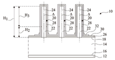
도 1은 마이크로와이어 또는 나노와이어를 구비하는 광전자 기기광전자 기기를 보이는 부분 개략 단면도; 그리고
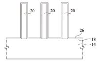
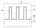
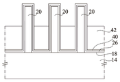
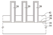
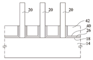
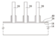
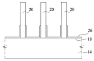
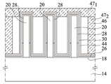
도 2a 내지 2p는 도 1의 광전자 기기를 제조하는 방법의 본 발명에 의한 실시예의 순차적인 단계들에서 얻어지는 구조들의 부분 개략 단면도들이다.
Claims (10)
- 기판(14)과 기판 상에 지지되는 마이크로와이어 또는 나노와이어(20)들을 구비하는 전자광전자 기기(10)를 제조하는 방법으로, 이 방법이:
a) 마이크로와이어 또는 나노와이어들을 절연층(26)으로 덮는 단계와;
b) 절연층을 불투명층(40)으로 덮는 단계와;
c) 와이어들 사이의 기판 상에 연장되는 제1 레지스트 층(42)을 적층시키는 단계와;
d) 제1 레지스트 층을 사진식각에 의해 제1 두께만큼 식각하는 단계와;
e) 단계 d)의 결과 남은 제1 레지스트 층을 플라즈마 식각에 의해 제2 두께만큼 식각하는 단계와;
f) 단계 e)의 결과 남은 제1 레지스트 층에 덮이지 않은 불투명층의 부분을 식각하는 단계와;
g) 불투명층으로 덮이지 않은 절연층의 부분을 식각하는 단계와;
h) 단계 e)의 결과 남은 제1 레지스트 층을 제거하는 단계와; 그리고
i) 불투명층을 제거하는 단계
들의 순차적인 단계들을 구비하는 전자기기의 제조방법. - 청구항 1에서,
마이크로와이어 또는 나노와이어(20)들의 높이가 250 nm 내지 50 μm의 범위에 있는
전자기기의 제조방법. - 청구항 1또는 2에서,
단계 c)에서의 제1 레지스트 층(42)의 최대 두께가 마이크로와이어 또는 나노와이어(20)들의 높이보다 더 큰
전자기기의 제조방법. - 청구항 1 내지 3 중의 어느 한 항에서,
절연층(26)의 두께가 5 nm 내지 1 μm의 범위에 있는
전자기기의 제조방법. - 청구항 1 내지 4 중의 어느 한 항에서,
플라즈마 식각이 산소 플라즈마 식각인
전자기기의 제조방법. - 청구항 1 내지 5 중의 어느 한 항에서,
불투명층(40)이 금속 또는 금속 합금으로 구성되는
전자기기의 제조방법. - 청구항 1 내지 6 중의 어느 한 항에서,
불투명층(40)의 두께가 5 nm 내지 1 μm의 범위에 있는
전자기기의 제조방법. - 청구항 1 내지 7 중의 어느 한 항에서, 단계 i) 이후에:
j) 각 마이크로와이어 또는 나노와이어(20)들의 절연층(26)으로 덮이지 않은 부분 상에 쉘(28)을 형성하는 단계로, 쉘이 전자기기에서 공급되거나 포착되는 복사의 대부분을 포착하거나 방출할 수 있는 활성 영역을 구비하는 단계와;
k) 쉘 상과 절연층 상에 전극층(30)을 형성하는 단계와;
l) 전극층을 도전층(44)으로 덮는 단계와;
m) 와이어들 사이의 도전층 상에 연장되는 제2 레지스트 층(46)을 적층시키는 단계와;
n) 제2 레지스트 층을 사진식각에 의해 구획하여 마이크로와이어 또는 나노와이어(20)들 상에 연장되는 레지스트 블록(48)을 형성하는 단계와;
o) 레지스트 블록을 플라즈마 식각에 의해 제3 두께만큼 식각하는 단계와;
p) 단계 o)의 결과로 남은 레지스트 블록으로 덮이지 않은 제2 반사성 도전층의 일부를 식각하는 단계와; 그리고
q) 단계 o)의 결과로 남은 제2 레지스트 층을 제거하는 단계
의 순차적인 단계들을 더 구비하는 전자기기의 제조방법. - 청구항 8에서, 단계 n)이:
r) 제2 레지스트 층(46)을 제4 두께만큼 부분적으로 노광시키는 단계와;
s) 마스킹 스크린을 사용하여 제2 레지스트 층의 부분을 전체 두께만큼 노광시키는 단계와; 그리고
t) 단계 r)과 s)에서 노광된 제2 레지스트 층의 부분들을 식각하는 단계
들을 포함하는 전자기기의 제조방법. - 청구항 8 또는 9에서,
도전층(44)이 반사성인
전자기기의 제조방법.
Applications Claiming Priority (3)
| Application Number | Priority Date | Filing Date | Title |
|---|---|---|---|
| FR1463372 | 2014-12-29 | ||
| FR1463372A FR3031242B1 (fr) | 2014-12-29 | 2014-12-29 | Procede de fabrication de nanofils ou de microfils semiconducteurs a pieds isoles |
| PCT/FR2015/053758 WO2016108023A1 (fr) | 2014-12-29 | 2015-12-24 | Procédé de fabrication de nanofils ou de microfils semiconducteurs a pieds isoles |
Publications (2)
| Publication Number | Publication Date |
|---|---|
| KR20170101242A true KR20170101242A (ko) | 2017-09-05 |
| KR102414850B1 KR102414850B1 (ko) | 2022-06-29 |
Family
ID=52779830
Family Applications (1)
| Application Number | Title | Priority Date | Filing Date |
|---|---|---|---|
| KR1020177019191A Active KR102414850B1 (ko) | 2014-12-29 | 2015-12-24 | 절연된 하부를 가지는 반도체 나노와이어 또는 마이크로와이어의 제조방법 |
Country Status (5)
| Country | Link |
|---|---|
| US (1) | US9954141B2 (ko) |
| EP (1) | EP3241246B1 (ko) |
| KR (1) | KR102414850B1 (ko) |
| FR (1) | FR3031242B1 (ko) |
| WO (1) | WO2016108023A1 (ko) |
Families Citing this family (6)
| Publication number | Priority date | Publication date | Assignee | Title |
|---|---|---|---|---|
| DE102015104144A1 (de) * | 2015-03-19 | 2016-09-22 | Osram Opto Semiconductors Gmbh | Optoelektronischer Halbleiterkörper und Verfahren zur Herstellung eines optoelektronischen Halbleiterkörpers |
| FR3068514B1 (fr) | 2017-06-30 | 2019-08-09 | Aledia | Dispositif optoelectronique |
| FR3076078B1 (fr) | 2017-12-27 | 2021-11-26 | Aledia | Dispositif optoelectronique a matrice de diodes tridimensionnelles |
| FR3093861B1 (fr) * | 2019-03-12 | 2021-09-17 | Commissariat Energie Atomique | Procédé d’enrobage de puces |
| FR3124024A1 (fr) * | 2021-06-11 | 2022-12-16 | Aledia | Procédé de fabrication d’un dispositif optoélectronique |
| FR3137498B1 (fr) | 2022-06-30 | 2025-03-28 | Aledia | Dispositif optoélectronique et procédé de fabrication d’un tel dispositif |
Citations (3)
| Publication number | Priority date | Publication date | Assignee | Title |
|---|---|---|---|---|
| KR100846514B1 (ko) * | 2007-02-05 | 2008-07-17 | 삼성전자주식회사 | 수직 구조물 상에 증착된 박막의 선택적 식각방법 및동방법을 이용한 메모리 소자의 제조방법 |
| WO2014064395A1 (fr) * | 2012-10-26 | 2014-05-01 | Aledia | Dispositif optoelectronique et son procede de fabrication |
| WO2014196920A1 (en) * | 2013-06-05 | 2014-12-11 | Sol Voltaics Ab | A solar cell structure and a method of its fabrication |
Family Cites Families (7)
| Publication number | Priority date | Publication date | Assignee | Title |
|---|---|---|---|---|
| FR1463372A (fr) | 1965-01-11 | 1966-12-23 | Moteur à combustion interne à piston rotatif | |
| CN101681813B (zh) | 2007-01-12 | 2012-07-11 | 昆南诺股份有限公司 | 氮化物纳米线及其制造方法 |
| WO2010062644A2 (en) | 2008-10-28 | 2010-06-03 | The Regents Of The University Of California | Vertical group iii-v nanowires on si, heterostructures, flexible arrays and fabrication |
| FR2995729B1 (fr) | 2012-09-18 | 2016-01-01 | Aledia | Dispositif opto-electrique a microfils ou nanofils semiconducteurs et son procede de fabrication |
| US9537044B2 (en) * | 2012-10-26 | 2017-01-03 | Aledia | Optoelectric device and method for manufacturing the same |
| US9500519B2 (en) * | 2012-12-03 | 2016-11-22 | Yale University | Superconducting single photon detector |
| US9773669B2 (en) * | 2014-09-11 | 2017-09-26 | Ramot At Tel-Aviv University Ltd. | Method of fabricating a nanoribbon and applications thereof |
-
2014
- 2014-12-29 FR FR1463372A patent/FR3031242B1/fr not_active Expired - Fee Related
-
2015
- 2015-12-24 KR KR1020177019191A patent/KR102414850B1/ko active Active
- 2015-12-24 EP EP15823722.2A patent/EP3241246B1/fr active Active
- 2015-12-24 US US15/538,148 patent/US9954141B2/en active Active
- 2015-12-24 WO PCT/FR2015/053758 patent/WO2016108023A1/fr not_active Ceased
Patent Citations (3)
| Publication number | Priority date | Publication date | Assignee | Title |
|---|---|---|---|---|
| KR100846514B1 (ko) * | 2007-02-05 | 2008-07-17 | 삼성전자주식회사 | 수직 구조물 상에 증착된 박막의 선택적 식각방법 및동방법을 이용한 메모리 소자의 제조방법 |
| WO2014064395A1 (fr) * | 2012-10-26 | 2014-05-01 | Aledia | Dispositif optoelectronique et son procede de fabrication |
| WO2014196920A1 (en) * | 2013-06-05 | 2014-12-11 | Sol Voltaics Ab | A solar cell structure and a method of its fabrication |
Also Published As
| Publication number | Publication date |
|---|---|
| US20180019376A1 (en) | 2018-01-18 |
| US9954141B2 (en) | 2018-04-24 |
| EP3241246A1 (fr) | 2017-11-08 |
| KR102414850B1 (ko) | 2022-06-29 |
| FR3031242A1 (fr) | 2016-07-01 |
| FR3031242B1 (fr) | 2016-12-30 |
| WO2016108023A1 (fr) | 2016-07-07 |
| EP3241246B1 (fr) | 2018-10-31 |
Similar Documents
| Publication | Publication Date | Title |
|---|---|---|
| KR102414850B1 (ko) | 절연된 하부를 가지는 반도체 나노와이어 또는 마이크로와이어의 제조방법 | |
| KR102060392B1 (ko) | 나노피라미드 크기의 광전자 구조 및 이를 제조하는 방법 | |
| US20110127554A1 (en) | Light emitting device and method of manufacturing the same | |
| WO2010071594A1 (en) | A nanostructured device | |
| KR102633272B1 (ko) | 발광 부품과 트랜지스터를 구비하는 광전자 소자 | |
| US20140014897A1 (en) | Semiconductor light emitting device with doped buffer layer and method of manufacturing the same | |
| CN107078186B (zh) | 具有三维半导体元件的光电设备 | |
| KR20220024162A (ko) | 발광 다이오드를 구비한 축형 광전자 장치 및 그 제조 방법 | |
| US10153399B2 (en) | Optoelectronic device comprising semiconductor elements and its fabrication process | |
| KR20100073757A (ko) | 마이크로 로드를 이용한 발광소자 및 그 제조방법 | |
| US10026870B2 (en) | Optoelectronic device having semiconductor elements | |
| EP3712963B1 (en) | Method of making a photoelectrode for solar water splitting | |
| KR101373398B1 (ko) | 고효율 발광다이오드 제조방법 | |
| US20170365737A1 (en) | Optoelectronic device comprising three-dimensional semiconductor elements and method for the production thereof | |
| US20190181329A1 (en) | Method to achieve active p-type layer/layers in iii-nitride epitaxial or device structures having buried p-type layers | |
| TWI437731B (zh) | 一種具有提升光取出率之半導體光電元件及其製造方法 | |
| KR101383161B1 (ko) | 발광 다이오드 및 그 제조 방법 | |
| KR20160003378A (ko) | 발광구조물 및 이를 포함하는 발광소자 | |
| KR100818459B1 (ko) | 발광소자 및 그의 제조방법 | |
| TWI714891B (zh) | 發光元件及其製造方法 | |
| KR20140036396A (ko) | 다공성 투명 전극을 포함하는 발광 다이오드 및 그 제조 방법 | |
| KR101171328B1 (ko) | 고효율 발광 다이오드 | |
| KR101403715B1 (ko) | 발광 소자 및 그 제조 방법 | |
| KR20130117735A (ko) | 고효율 발광다이오드 제조방법 |
Legal Events
| Date | Code | Title | Description |
|---|---|---|---|
| PA0105 | International application |
St.27 status event code: A-0-1-A10-A15-nap-PA0105 |
|
| PG1501 | Laying open of application |
St.27 status event code: A-1-1-Q10-Q12-nap-PG1501 |
|
| R18-X000 | Changes to party contact information recorded |
St.27 status event code: A-3-3-R10-R18-oth-X000 |
|
| A201 | Request for examination | ||
| PA0201 | Request for examination |
St.27 status event code: A-1-2-D10-D11-exm-PA0201 |
|
| R18-X000 | Changes to party contact information recorded |
St.27 status event code: A-3-3-R10-R18-oth-X000 |
|
| D13-X000 | Search requested |
St.27 status event code: A-1-2-D10-D13-srh-X000 |
|
| D14-X000 | Search report completed |
St.27 status event code: A-1-2-D10-D14-srh-X000 |
|
| E902 | Notification of reason for refusal | ||
| PE0902 | Notice of grounds for rejection |
St.27 status event code: A-1-2-D10-D21-exm-PE0902 |
|
| P11-X000 | Amendment of application requested |
St.27 status event code: A-2-2-P10-P11-nap-X000 |
|
| P13-X000 | Application amended |
St.27 status event code: A-2-2-P10-P13-nap-X000 |
|
| E701 | Decision to grant or registration of patent right | ||
| PE0701 | Decision of registration |
St.27 status event code: A-1-2-D10-D22-exm-PE0701 |
|
| GRNT | Written decision to grant | ||
| PR0701 | Registration of establishment |
St.27 status event code: A-2-4-F10-F11-exm-PR0701 |
|
| PR1002 | Payment of registration fee |
St.27 status event code: A-2-2-U10-U12-oth-PR1002 Fee payment year number: 1 |
|
| PG1601 | Publication of registration |
St.27 status event code: A-4-4-Q10-Q13-nap-PG1601 |
|
| P22-X000 | Classification modified |
St.27 status event code: A-4-4-P10-P22-nap-X000 |
|
| PR1001 | Payment of annual fee |
St.27 status event code: A-4-4-U10-U11-oth-PR1001 Fee payment year number: 4 |
|
| R18 | Changes to party contact information recorded |
Free format text: ST27 STATUS EVENT CODE: A-5-5-R10-R18-OTH-X000 (AS PROVIDED BY THE NATIONAL OFFICE) |
|
| R18-X000 | Changes to party contact information recorded |
St.27 status event code: A-5-5-R10-R18-oth-X000 |
|
| R18 | Changes to party contact information recorded |
Free format text: ST27 STATUS EVENT CODE: A-5-5-R10-R18-OTH-X000 (AS PROVIDED BY THE NATIONAL OFFICE) |
|
| R18-X000 | Changes to party contact information recorded |
St.27 status event code: A-5-5-R10-R18-oth-X000 |