KR20170105480A - 스핀-온 하드마스크 재료 - Google Patents
스핀-온 하드마스크 재료 Download PDFInfo
- Publication number
- KR20170105480A KR20170105480A KR1020177012083A KR20177012083A KR20170105480A KR 20170105480 A KR20170105480 A KR 20170105480A KR 1020177012083 A KR1020177012083 A KR 1020177012083A KR 20177012083 A KR20177012083 A KR 20177012083A KR 20170105480 A KR20170105480 A KR 20170105480A
- Authority
- KR
- South Korea
- Prior art keywords
- resin
- organic sulfonic
- composition
- sulfonic acids
- spin
- Prior art date
- Legal status (The legal status is an assumption and is not a legal conclusion. Google has not performed a legal analysis and makes no representation as to the accuracy of the status listed.)
- Granted
Links
Images


Classifications
-
- G—PHYSICS
- G03—PHOTOGRAPHY; CINEMATOGRAPHY; ANALOGOUS TECHNIQUES USING WAVES OTHER THAN OPTICAL WAVES; ELECTROGRAPHY; HOLOGRAPHY
- G03F—PHOTOMECHANICAL PRODUCTION OF TEXTURED OR PATTERNED SURFACES, e.g. FOR PRINTING, FOR PROCESSING OF SEMICONDUCTOR DEVICES; MATERIALS THEREFOR; ORIGINALS THEREFOR; APPARATUS SPECIALLY ADAPTED THEREFOR
- G03F7/00—Photomechanical, e.g. photolithographic, production of textured or patterned surfaces, e.g. printing surfaces; Materials therefor, e.g. comprising photoresists; Apparatus specially adapted therefor
- G03F7/004—Photosensitive materials
-
- C—CHEMISTRY; METALLURGY
- C01—INORGANIC CHEMISTRY
- C01B—NON-METALLIC ELEMENTS; COMPOUNDS THEREOF; METALLOIDS OR COMPOUNDS THEREOF NOT COVERED BY SUBCLASS C01C
- C01B32/00—Carbon; Compounds thereof
- C01B32/15—Nano-sized carbon materials
- C01B32/152—Fullerenes
- C01B32/156—After-treatment
-
- B—PERFORMING OPERATIONS; TRANSPORTING
- B05—SPRAYING OR ATOMISING IN GENERAL; APPLYING FLUENT MATERIALS TO SURFACES, IN GENERAL
- B05D—PROCESSES FOR APPLYING FLUENT MATERIALS TO SURFACES, IN GENERAL
- B05D1/00—Processes for applying liquids or other fluent materials
- B05D1/002—Processes for applying liquids or other fluent materials the substrate being rotated
- B05D1/005—Spin coating
-
- B—PERFORMING OPERATIONS; TRANSPORTING
- B05—SPRAYING OR ATOMISING IN GENERAL; APPLYING FLUENT MATERIALS TO SURFACES, IN GENERAL
- B05D—PROCESSES FOR APPLYING FLUENT MATERIALS TO SURFACES, IN GENERAL
- B05D3/00—Pretreatment of surfaces to which liquids or other fluent materials are to be applied; After-treatment of applied coatings, e.g. intermediate treating of an applied coating preparatory to subsequent applications of liquids or other fluent materials
- B05D3/002—Pretreatement
-
- B—PERFORMING OPERATIONS; TRANSPORTING
- B05—SPRAYING OR ATOMISING IN GENERAL; APPLYING FLUENT MATERIALS TO SURFACES, IN GENERAL
- B05D—PROCESSES FOR APPLYING FLUENT MATERIALS TO SURFACES, IN GENERAL
- B05D3/00—Pretreatment of surfaces to which liquids or other fluent materials are to be applied; After-treatment of applied coatings, e.g. intermediate treating of an applied coating preparatory to subsequent applications of liquids or other fluent materials
- B05D3/02—Pretreatment of surfaces to which liquids or other fluent materials are to be applied; After-treatment of applied coatings, e.g. intermediate treating of an applied coating preparatory to subsequent applications of liquids or other fluent materials by baking
- B05D3/0254—After-treatment
-
- C—CHEMISTRY; METALLURGY
- C09—DYES; PAINTS; POLISHES; NATURAL RESINS; ADHESIVES; COMPOSITIONS NOT OTHERWISE PROVIDED FOR; APPLICATIONS OF MATERIALS NOT OTHERWISE PROVIDED FOR
- C09D—COATING COMPOSITIONS, e.g. PAINTS, VARNISHES OR LACQUERS; FILLING PASTES; CHEMICAL PAINT OR INK REMOVERS; INKS; CORRECTING FLUIDS; WOODSTAINS; PASTES OR SOLIDS FOR COLOURING OR PRINTING; USE OF MATERIALS THEREFOR
- C09D163/00—Coating compositions based on epoxy resins; Coating compositions based on derivatives of epoxy resins
- C09D163/04—Epoxynovolacs
-
- C—CHEMISTRY; METALLURGY
- C09—DYES; PAINTS; POLISHES; NATURAL RESINS; ADHESIVES; COMPOSITIONS NOT OTHERWISE PROVIDED FOR; APPLICATIONS OF MATERIALS NOT OTHERWISE PROVIDED FOR
- C09D—COATING COMPOSITIONS, e.g. PAINTS, VARNISHES OR LACQUERS; FILLING PASTES; CHEMICAL PAINT OR INK REMOVERS; INKS; CORRECTING FLUIDS; WOODSTAINS; PASTES OR SOLIDS FOR COLOURING OR PRINTING; USE OF MATERIALS THEREFOR
- C09D177/00—Coating compositions based on polyamides obtained by reactions forming a carboxylic amide link in the main chain; Coating compositions based on derivatives of such polymers
-
- G—PHYSICS
- G03—PHOTOGRAPHY; CINEMATOGRAPHY; ANALOGOUS TECHNIQUES USING WAVES OTHER THAN OPTICAL WAVES; ELECTROGRAPHY; HOLOGRAPHY
- G03F—PHOTOMECHANICAL PRODUCTION OF TEXTURED OR PATTERNED SURFACES, e.g. FOR PRINTING, FOR PROCESSING OF SEMICONDUCTOR DEVICES; MATERIALS THEREFOR; ORIGINALS THEREFOR; APPARATUS SPECIALLY ADAPTED THEREFOR
- G03F7/00—Photomechanical, e.g. photolithographic, production of textured or patterned surfaces, e.g. printing surfaces; Materials therefor, e.g. comprising photoresists; Apparatus specially adapted therefor
- G03F7/004—Photosensitive materials
- G03F7/0048—Photosensitive materials characterised by the solvents or agents facilitating spreading, e.g. tensio-active agents
-
- G—PHYSICS
- G03—PHOTOGRAPHY; CINEMATOGRAPHY; ANALOGOUS TECHNIQUES USING WAVES OTHER THAN OPTICAL WAVES; ELECTROGRAPHY; HOLOGRAPHY
- G03F—PHOTOMECHANICAL PRODUCTION OF TEXTURED OR PATTERNED SURFACES, e.g. FOR PRINTING, FOR PROCESSING OF SEMICONDUCTOR DEVICES; MATERIALS THEREFOR; ORIGINALS THEREFOR; APPARATUS SPECIALLY ADAPTED THEREFOR
- G03F7/00—Photomechanical, e.g. photolithographic, production of textured or patterned surfaces, e.g. printing surfaces; Materials therefor, e.g. comprising photoresists; Apparatus specially adapted therefor
- G03F7/004—Photosensitive materials
- G03F7/09—Photosensitive materials characterised by structural details, e.g. supports, auxiliary layers
- G03F7/11—Photosensitive materials characterised by structural details, e.g. supports, auxiliary layers having cover layers or intermediate layers, e.g. subbing layers
-
- H—ELECTRICITY
- H10—SEMICONDUCTOR DEVICES; ELECTRIC SOLID-STATE DEVICES NOT OTHERWISE PROVIDED FOR
- H10P—GENERIC PROCESSES OR APPARATUS FOR THE MANUFACTURE OR TREATMENT OF DEVICES COVERED BY CLASS H10
- H10P14/00—Formation of materials, e.g. in the shape of layers or pillars
- H10P14/60—Formation of materials, e.g. in the shape of layers or pillars of insulating materials
- H10P14/63—Formation of materials, e.g. in the shape of layers or pillars of insulating materials characterised by the formation processes
- H10P14/6326—Deposition processes
- H10P14/6342—Liquid deposition, e.g. spin-coating, sol-gel techniques or spray coating
-
- H—ELECTRICITY
- H10—SEMICONDUCTOR DEVICES; ELECTRIC SOLID-STATE DEVICES NOT OTHERWISE PROVIDED FOR
- H10P—GENERIC PROCESSES OR APPARATUS FOR THE MANUFACTURE OR TREATMENT OF DEVICES COVERED BY CLASS H10
- H10P14/00—Formation of materials, e.g. in the shape of layers or pillars
- H10P14/60—Formation of materials, e.g. in the shape of layers or pillars of insulating materials
- H10P14/65—Formation of materials, e.g. in the shape of layers or pillars of insulating materials characterised by treatments performed before or after the formation of the materials
- H10P14/6516—Formation of materials, e.g. in the shape of layers or pillars of insulating materials characterised by treatments performed before or after the formation of the materials of treatments performed after formation of the materials
-
- H—ELECTRICITY
- H10—SEMICONDUCTOR DEVICES; ELECTRIC SOLID-STATE DEVICES NOT OTHERWISE PROVIDED FOR
- H10P—GENERIC PROCESSES OR APPARATUS FOR THE MANUFACTURE OR TREATMENT OF DEVICES COVERED BY CLASS H10
- H10P14/00—Formation of materials, e.g. in the shape of layers or pillars
- H10P14/60—Formation of materials, e.g. in the shape of layers or pillars of insulating materials
- H10P14/69—Inorganic materials
- H10P14/6902—Inorganic materials composed of carbon, e.g. alpha-C, diamond or hydrogen doped carbon
-
- H—ELECTRICITY
- H10—SEMICONDUCTOR DEVICES; ELECTRIC SOLID-STATE DEVICES NOT OTHERWISE PROVIDED FOR
- H10P—GENERIC PROCESSES OR APPARATUS FOR THE MANUFACTURE OR TREATMENT OF DEVICES COVERED BY CLASS H10
- H10P50/00—Etching of wafers, substrates or parts of devices
- H10P50/20—Dry etching; Plasma etching; Reactive-ion etching
- H10P50/24—Dry etching; Plasma etching; Reactive-ion etching of semiconductor materials
- H10P50/242—Dry etching; Plasma etching; Reactive-ion etching of semiconductor materials of Group IV materials
-
- H—ELECTRICITY
- H10—SEMICONDUCTOR DEVICES; ELECTRIC SOLID-STATE DEVICES NOT OTHERWISE PROVIDED FOR
- H10P—GENERIC PROCESSES OR APPARATUS FOR THE MANUFACTURE OR TREATMENT OF DEVICES COVERED BY CLASS H10
- H10P50/00—Etching of wafers, substrates or parts of devices
- H10P50/20—Dry etching; Plasma etching; Reactive-ion etching
- H10P50/28—Dry etching; Plasma etching; Reactive-ion etching of insulating materials
- H10P50/282—Dry etching; Plasma etching; Reactive-ion etching of insulating materials of inorganic materials
- H10P50/283—Dry etching; Plasma etching; Reactive-ion etching of insulating materials of inorganic materials by chemical means
- H10P50/285—Dry etching; Plasma etching; Reactive-ion etching of insulating materials of inorganic materials by chemical means of materials not containing Si, e.g. PZT or Al2O3
-
- H—ELECTRICITY
- H10—SEMICONDUCTOR DEVICES; ELECTRIC SOLID-STATE DEVICES NOT OTHERWISE PROVIDED FOR
- H10P—GENERIC PROCESSES OR APPARATUS FOR THE MANUFACTURE OR TREATMENT OF DEVICES COVERED BY CLASS H10
- H10P50/00—Etching of wafers, substrates or parts of devices
- H10P50/20—Dry etching; Plasma etching; Reactive-ion etching
- H10P50/28—Dry etching; Plasma etching; Reactive-ion etching of insulating materials
- H10P50/286—Dry etching; Plasma etching; Reactive-ion etching of insulating materials of organic materials
- H10P50/287—Dry etching; Plasma etching; Reactive-ion etching of insulating materials of organic materials by chemical means
-
- H—ELECTRICITY
- H10—SEMICONDUCTOR DEVICES; ELECTRIC SOLID-STATE DEVICES NOT OTHERWISE PROVIDED FOR
- H10P—GENERIC PROCESSES OR APPARATUS FOR THE MANUFACTURE OR TREATMENT OF DEVICES COVERED BY CLASS H10
- H10P50/00—Etching of wafers, substrates or parts of devices
- H10P50/69—Etching of wafers, substrates or parts of devices using masks for semiconductor materials
- H10P50/691—Etching of wafers, substrates or parts of devices using masks for semiconductor materials for Group V materials or Group III-V materials
- H10P50/692—Etching of wafers, substrates or parts of devices using masks for semiconductor materials for Group V materials or Group III-V materials characterised by their composition, e.g. multilayer masks or materials
-
- H—ELECTRICITY
- H10—SEMICONDUCTOR DEVICES; ELECTRIC SOLID-STATE DEVICES NOT OTHERWISE PROVIDED FOR
- H10P—GENERIC PROCESSES OR APPARATUS FOR THE MANUFACTURE OR TREATMENT OF DEVICES COVERED BY CLASS H10
- H10P76/00—Manufacture or treatment of masks on semiconductor bodies, e.g. by lithography or photolithography
- H10P76/20—Manufacture or treatment of masks on semiconductor bodies, e.g. by lithography or photolithography of masks comprising organic materials
- H10P76/204—Manufacture or treatment of masks on semiconductor bodies, e.g. by lithography or photolithography of masks comprising organic materials of organic photoresist masks
- H10P76/2041—Photolithographic processes
Landscapes
- Chemical & Material Sciences (AREA)
- Organic Chemistry (AREA)
- Engineering & Computer Science (AREA)
- Materials Engineering (AREA)
- Physics & Mathematics (AREA)
- General Physics & Mathematics (AREA)
- Life Sciences & Earth Sciences (AREA)
- Wood Science & Technology (AREA)
- Nanotechnology (AREA)
- Inorganic Chemistry (AREA)
- Chemical Kinetics & Catalysis (AREA)
- Structural Engineering (AREA)
- Architecture (AREA)
- Materials For Photolithography (AREA)
- Organic Low-Molecular-Weight Compounds And Preparation Thereof (AREA)
- Compositions Of Macromolecular Compounds (AREA)
- Exposure Of Semiconductors, Excluding Electron Or Ion Beam Exposure (AREA)
- Plasma & Fusion (AREA)
Abstract
Description
도 2는 본 명세서에 기술된 재료로 하드마스크 막을 형성하고, 이 막을 가열하고 용매 침지를 수행한 결과를 도시한다.
도 3은 도 1에 도시된 방식에 따라 약 100 nm의 탄소로 에칭된 25 nm 라인들 및 공간들을 도시한다.










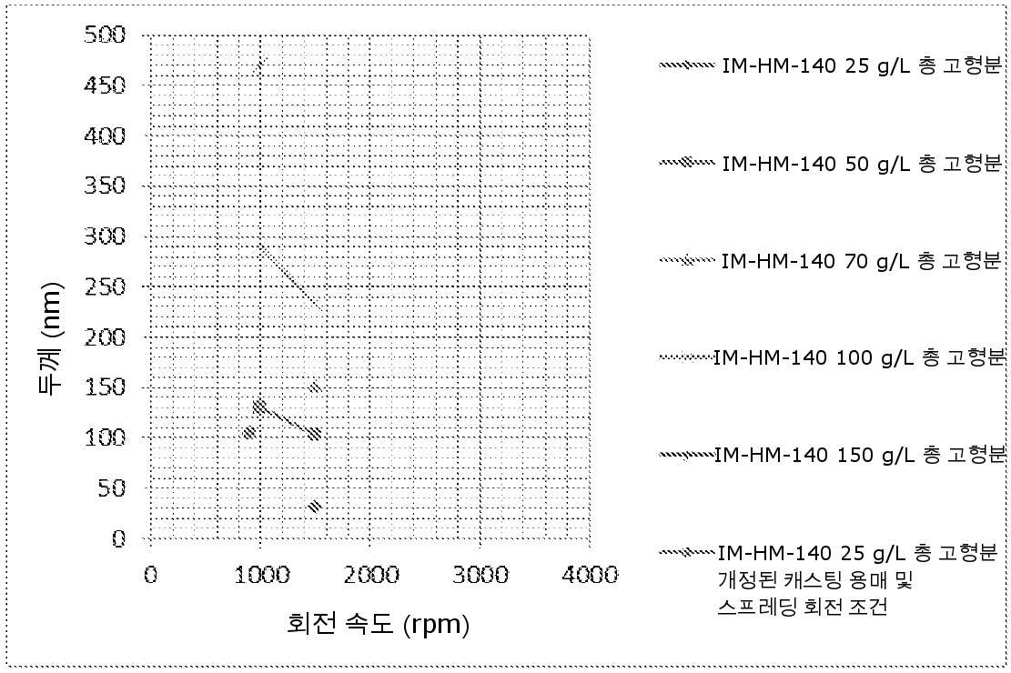
| 스핀-온 탄소 하드마스크 데이타 시트 | ||
| 변형예: IM-HM-120 | 탄소 함량(wt%): 84% | |
| 에칭(ICP, SF6/C4F8) | 에칭 속도(nm/s) 에칭 기법 실리콘에 대한 선택도 대조군 레지스트 대조군 에칭 속도 |
0.98 nm/s ICP 혼합 모드 에칭 4.5:1 SAL601 1.24 nm/s |
| 에칭(ICP, SF6/CHF3) | 에칭 속도(nm/s) 에칭 기법 실리콘에 대한 선택도 대조군 레지스트 대조군 에칭 속도 |
0.8 nm/s ICP 혼합 모드 에칭 14.8:1 SAL601 1.34 nm/s |
| 용매 상용성(코팅) | 캐스팅 용매 캐스팅 가능한 두께 (사이클로헥사논) 이용가능한 기타 용매 선택지가 있음 |
사이클로헥사논 130 nm 까지 1.3 ㎛ 까지의 다층이 제조되었음(다른 용매로부터) |
| 용매 상용성 (경화 후 용출) |
두께 손실 (PGME, PGMEA) 두께 손실 (에틸 락테이트) 두께 손실 (EEP, 아니솔) 두께 손실 (MCB) 두께 손실 (사이클로헥사논) 두께 손실 (TMAH 25%) |
1분 침지후 용해 없음 1분 침지후 용해 없음 1분 침지후 용해 없음 1분 침지후 용해 없음 1분 침지후 용해 없음 1분 침지후 용해 없음 |
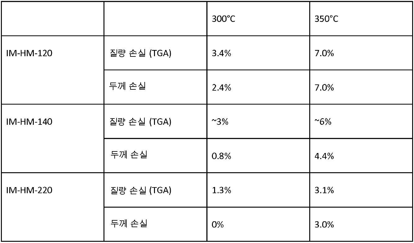
| 열특성(N2 분위기) | 두께 손실 질량 손실(TGA) |
두께 손실(%)@300 ℃ → 5분 후 2.4% 두께 손실(%)@350 ℃ → 5분 후 7.0% 두께 손실(%)@400 ℃ → 5분 후 14.2% 질량 손실(%)@300 ℃→3.4% 질량 손실(%)@350 ℃→7.0% 질량 손실(%)@400 ℃→14.2% |
| 영률 | 300 ℃ 베이킹 후, 1 ㎛ 막 | 4.7 GPa (환산 모듈러스) |
| 경도 | 300 ℃ 베이킹 후, 1 ㎛ 막 | 1.15 GPa |
| 조도 | 기재 평균 조도 RMS 조도 피크로부터 골짜기 까지의 깊이 |
미코팅 실리콘 / SoC-코팅된 Si 0.28 nm / 0.28 nm 0.35 nm / 0.36 nm 4.57 nm / 3.12 nm |
| 이미지 왼쪽: 풀러렌 하드마스크 내로 전사된 30 nm 라인 오른쪽: 실리콘 내로 에칭된 저밀도 20 nm 라인 |
 |
|


Claims (14)
- 풀러렌 유도체 및 가교제를 포함하는 스핀-온 하드마스크 형성용 조성물로서,
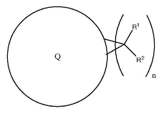
상기 풀러렌 유도체는 하기 화학식 (I)로 표시되고:
<화학식 (I)>
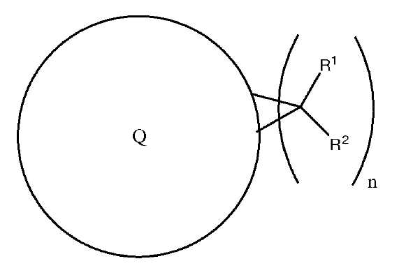
여기서, n은 1 내지 6의 정수이고, 풀러렌 내 탄소원자 개수인 Q는 60, 70, 76, 78, 80, 82 또는 84이고, R1은 에스테르, 알코올, 페놀, 아민, 아미드, 이미드 또는 카르복실산을 포함하는 제1 치환기를 나타내고, R2는 수소, 할로겐, C6-C20 아릴기, C1-C20 알킬기, 에스테르, 알코올, 페놀, 아민, 아미드, 이미드 또는 카르복실산을 포함하는 제2 치환기를 나타내며,
상기 가교제는 둘 이상의 열적 또는 촉매적 반응성 기를 포함하는,
조성물. - 제 1 항에 있어서, 상기 조성물은 하나 이상의 추가 풀러렌 유도체를 더 포함하고, 적어도 하나의 Q는 60이고, 적어도 하나의 제2 Q는 70인, 조성물.
- 제 2 항에 있어서, 하나 이상의 열적 산 발생제를 더 포함하는 조성물.
- 제 2 항에 있어서, R1은 카르복실산인, 조성물.
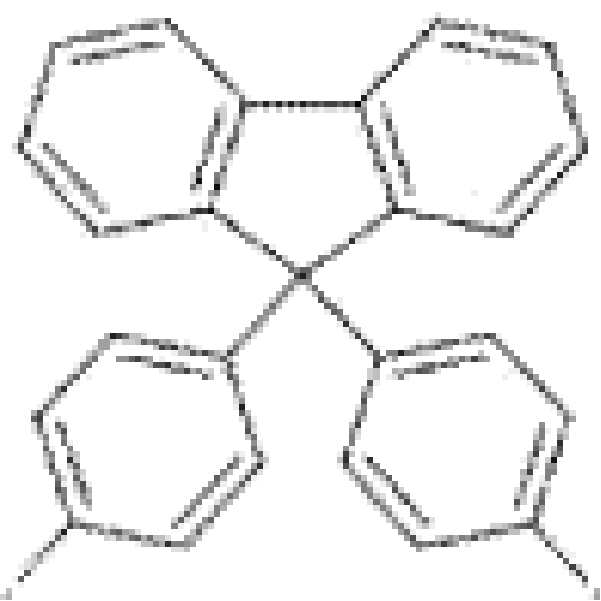
- 제 4 항에 있어서, 상기 가교제는 폴리아로마틱 디아민(polyaromatic diamine)인, 조성물.
- 제 5 항에 있어서, 상기 폴리아로마틱 디아민은 4,4'-(9-플루오레닐리덴)디아닐린인, 조성물.
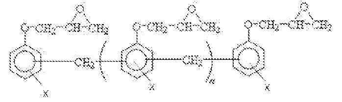
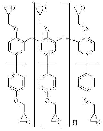
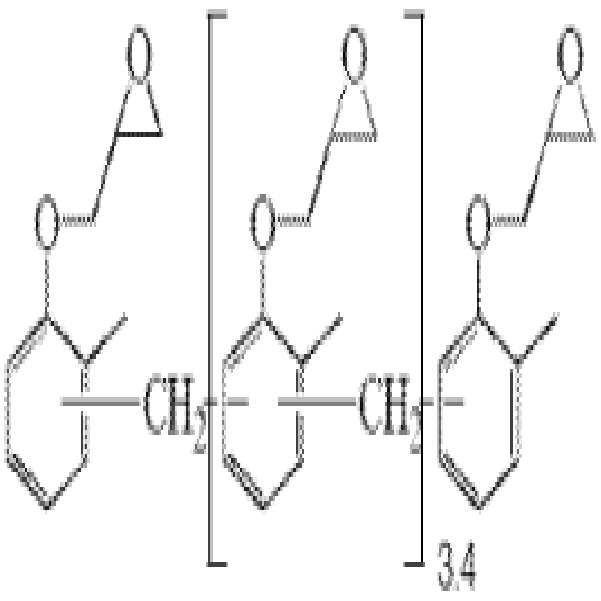
- 제 2 항에 있어서, 상기 가교제는, 에폭시 페놀계 노볼락 수지, 에폭시 크레실계 노볼락 수지, 에폭시 비스페놀 A 수지, 에폭시 비스페놀 A 노볼락 수지, 에폭시 비스페놀 C 수지, 알킬올메틸 멜라민 수지, 알킬올메틸 글리콜루릴 수지, 알킬올메틸 구아나민 수지, 알킬올메틸 벤조-구아나민 수지, 글리코실 요소 수지, 또는 알키드 수지로부터 선택되는, 조성물.
- 제 7 항에 있어서, 하나 이상의 열적 산 발생제를 더 포함하는 조성물.
- 제 8 항에 있어서, 상기 하나 이상의 열적 산 발생제는, 유기 술폰산의 알킬 에스테르, 유기 술폰산의 지환족 에스테르, 유기 술폰산의 아민 염, 유기 술폰산의 2-니트로벤질 에스테르, 유기 술폰산의 4-니트로벤질 에스테르, 유기 술폰산의 벤조인 에스테르, 유기 술폰산의 β-하이드록시알킬 에스테르, 유기 술폰산의 β-하이드록시사이클로알킬 에스테르, 유기 술폰산의 트리아릴 술포늄염, 유기 술폰산의 알킬 디아릴 술포늄염, 유기 술폰산의 디알킬 아릴 술포늄염, 유기 술폰산의 트리알킬 술포늄염, 유기 술폰산의 디아릴 요오도늄염, 유기 술폰산의 알킬 아릴 술포늄염, 또는 트리스(오르가노술포닐)메티드의 암모늄염으로부터 선택되는, 조성물.
- 제 7 항에 있어서, 하나 이상의 광산 발생제를 더 포함하는 조성물.
- 제 10 항에 있어서, 상기 하나 이상의 광산 발생제는, 할로겐화 트리아진, 유기 술폰산의 2-니트로벤질 에스테르, 유기 술폰산의 4-니트로벤질 에스테르, 유기 술폰산의 트리아릴 술포늄염, 유기 술폰산의 알킬 디아릴 술포늄염, 유기 술폰산의 디알킬 아릴 술포늄염, 유기 술폰산의 디아릴 요오도늄염, 유기 술폰산의 알킬 아릴 술포늄염, n-오르가노술포닐 옥시바이사이클로[2.2.1]-헵트-5-엔-2,3-디카르복시이미드, 또는 1,3-디옥소이소인돌린-2-일 유기술포네이트로부터 선택되는, 조성물.
- 제 7 항에 있어서, 상기 가교제는, 에폭시화 페놀계 수지, 에폭시화 크레실계 수지, 에폭시화 비스페놀 A 수지, 에폭시화 비스페놀 A 노볼락 수지, 에폭시 비스페놀 수지, 알킬올메틸 멜라민 수지, 알킬올메틸 글리콜루릴 수지, 알킬올메틸 구아나민 수지, 알킬올메틸 벤조-구아나민 수지, 글리코실 요소 수지, 또는 이소시아네이트 수지로부터 선택되는, 조성물.
- 제 7 항에 있어서, 상기 스핀-온 하드마스크는, 폴리에틸렌 글리콜 모노메틸 에테르 아세테이트, 에틸 락테이트, 아니솔, 톨루엔, 클로로포름, 클로로벤젠, o-디클로로벤젠, m-디클로로벤젠, p-디클로로벤젠, o-크실렌, m-크실렌, p-크실렌, 이황화탄소 또는 이들의 조합으로부터 선택되는 하나 이상의 용매를 더 포함하는, 조성물.
- a) 제 1 항 내지 제 13 항 중 어느 한 항에 따른 조성물을 제공하는 단계;
b) 코팅을 기재 상에 형성하는 단계; 및
c) 상기 기재 및 상기 코팅을, 상기 코팅을 가교결합시키기에 충분한 온도에서, 가열하는 단계;를 포함하는 스핀-온 하드마스크 형성 방법.
Applications Claiming Priority (3)
| Application Number | Priority Date | Filing Date | Title |
|---|---|---|---|
| US201462061294P | 2014-10-08 | 2014-10-08 | |
| US62/061,294 | 2014-10-08 | ||
| PCT/US2015/064089 WO2016058008A2 (en) | 2014-10-08 | 2015-12-04 | Spin on hard-mask material |
Publications (2)
| Publication Number | Publication Date |
|---|---|
| KR20170105480A true KR20170105480A (ko) | 2017-09-19 |
| KR102514100B1 KR102514100B1 (ko) | 2023-03-24 |
Family
ID=55653963
Family Applications (1)
| Application Number | Title | Priority Date | Filing Date |
|---|---|---|---|
| KR1020177012083A Active KR102514100B1 (ko) | 2014-10-08 | 2015-12-04 | 스핀-온 하드마스크 재료 |
Country Status (5)
| Country | Link |
|---|---|
| US (1) | US10290500B2 (ko) |
| JP (1) | JP6967967B2 (ko) |
| KR (1) | KR102514100B1 (ko) |
| CN (1) | CN107207259A (ko) |
| WO (1) | WO2016058008A2 (ko) |
Cited By (3)
| Publication number | Priority date | Publication date | Assignee | Title |
|---|---|---|---|---|
| KR20200104564A (ko) * | 2019-02-27 | 2020-09-04 | 동우 화인켐 주식회사 | 하드마스크용 조성물 |
| KR20200125662A (ko) * | 2018-02-25 | 2020-11-04 | 알렉스 필립 그레이엄 로빈손 | 하드 마스크(hard mask) 조성물 |
| KR20220021315A (ko) * | 2020-08-13 | 2022-02-22 | 삼성에스디아이 주식회사 | 하드마스크 조성물 및 패턴 형성 방법 |
Families Citing this family (3)
| Publication number | Priority date | Publication date | Assignee | Title |
|---|---|---|---|---|
| KR102675775B1 (ko) | 2016-12-27 | 2024-06-18 | 삼성전자주식회사 | 하드마스크 조성물, 이를 이용한 패턴의 형성방법 및 상기 하드마스크 조성물을 이용하여 형성된 하드마스크 |
| US10475991B2 (en) | 2018-02-22 | 2019-11-12 | Taiwan Semiconductor Manufacturing Company, Ltd. | Fabrication of large height top metal electrode for sub-60nm magnetoresistive random access memory (MRAM) devices |
| CN109461817B (zh) * | 2018-09-20 | 2020-05-12 | 中国科学院半导体研究所 | 在卤化物钙钛矿薄膜表面制作金属微纳结构的方法 |
Citations (4)
| Publication number | Priority date | Publication date | Assignee | Title |
|---|---|---|---|---|
| JP2004264710A (ja) * | 2003-03-04 | 2004-09-24 | Jsr Corp | 反射防止膜形成組成物および反射防止膜 |
| JP2004279694A (ja) * | 2003-03-14 | 2004-10-07 | Nippon Telegr & Teleph Corp <Ntt> | レジスト組成物およびその硬化方法 |
| KR20110091479A (ko) * | 2010-02-05 | 2011-08-11 | 신에쓰 가가꾸 고교 가부시끼가이샤 | 레지스트 하층막 재료, 레지스트 하층막 형성 방법, 패턴 형성 방법, 풀러렌 유도체 |
| KR20150028221A (ko) * | 2012-02-10 | 2015-03-13 | 더 유니버시티 오브 버밍험 | 스핀 온 하드-마스크 재료 |
Family Cites Families (11)
| Publication number | Priority date | Publication date | Assignee | Title |
|---|---|---|---|---|
| JPH07306531A (ja) * | 1994-05-11 | 1995-11-21 | Japan Synthetic Rubber Co Ltd | 感放射線性樹脂組成物 |
| US7264617B2 (en) * | 2000-02-29 | 2007-09-04 | Alex Freeman | Integrally manufactured micro-electrofluidic cables |
| JPWO2003079475A1 (ja) * | 2002-03-20 | 2005-07-21 | 株式会社三昌化工 | 燃料電池用セパレータ、その製造方法および該燃料電池用セパレータを用いた燃料電池 |
| JP4496432B2 (ja) * | 2005-02-18 | 2010-07-07 | 信越化学工業株式会社 | フォトレジスト下層膜形成材料及びパターン形成方法 |
| US8361694B2 (en) * | 2007-04-06 | 2013-01-29 | Nissan Chemical Industries, Ltd. | Resist underlayer film forming composition |
| US8592134B2 (en) * | 2007-12-07 | 2013-11-26 | Mitsubishi Gas Chemical Company, Inc. | Composition for forming base film for lithography and method for forming multilayer resist pattern |
| GB0920231D0 (en) * | 2009-11-18 | 2010-01-06 | Univ Birmingham | Photoresist composition |
| JP5757286B2 (ja) * | 2010-03-01 | 2015-07-29 | 日産化学工業株式会社 | フラーレン誘導体を含むレジスト下層膜形成組成物 |
| US9383646B2 (en) * | 2014-02-24 | 2016-07-05 | Irresistible Materials Ltd | Two-step photoresist compositions and methods |
| US9255172B1 (en) * | 2014-08-05 | 2016-02-09 | International Business Machines Corporation | High-performance, filler-reinforced, recyclable composite materials |
| JP6628052B2 (ja) * | 2015-03-11 | 2020-01-08 | 日産化学株式会社 | レジスト下層膜の形成方法 |
-
2015
- 2015-12-04 US US15/511,416 patent/US10290500B2/en active Active
- 2015-12-04 CN CN201580054194.6A patent/CN107207259A/zh active Pending
- 2015-12-04 JP JP2017519309A patent/JP6967967B2/ja active Active
- 2015-12-04 KR KR1020177012083A patent/KR102514100B1/ko active Active
- 2015-12-04 WO PCT/US2015/064089 patent/WO2016058008A2/en not_active Ceased
Patent Citations (4)
| Publication number | Priority date | Publication date | Assignee | Title |
|---|---|---|---|---|
| JP2004264710A (ja) * | 2003-03-04 | 2004-09-24 | Jsr Corp | 反射防止膜形成組成物および反射防止膜 |
| JP2004279694A (ja) * | 2003-03-14 | 2004-10-07 | Nippon Telegr & Teleph Corp <Ntt> | レジスト組成物およびその硬化方法 |
| KR20110091479A (ko) * | 2010-02-05 | 2011-08-11 | 신에쓰 가가꾸 고교 가부시끼가이샤 | 레지스트 하층막 재료, 레지스트 하층막 형성 방법, 패턴 형성 방법, 풀러렌 유도체 |
| KR20150028221A (ko) * | 2012-02-10 | 2015-03-13 | 더 유니버시티 오브 버밍험 | 스핀 온 하드-마스크 재료 |
Cited By (3)
| Publication number | Priority date | Publication date | Assignee | Title |
|---|---|---|---|---|
| KR20200125662A (ko) * | 2018-02-25 | 2020-11-04 | 알렉스 필립 그레이엄 로빈손 | 하드 마스크(hard mask) 조성물 |
| KR20200104564A (ko) * | 2019-02-27 | 2020-09-04 | 동우 화인켐 주식회사 | 하드마스크용 조성물 |
| KR20220021315A (ko) * | 2020-08-13 | 2022-02-22 | 삼성에스디아이 주식회사 | 하드마스크 조성물 및 패턴 형성 방법 |
Also Published As
| Publication number | Publication date |
|---|---|
| CN107207259A (zh) | 2017-09-26 |
| US10290500B2 (en) | 2019-05-14 |
| JP6967967B2 (ja) | 2021-11-17 |
| WO2016058008A3 (en) | 2016-05-26 |
| JP2017533464A (ja) | 2017-11-09 |
| KR102514100B1 (ko) | 2023-03-24 |
| WO2016058008A2 (en) | 2016-04-14 |
| US20170278703A1 (en) | 2017-09-28 |
Similar Documents
| Publication | Publication Date | Title |
|---|---|---|
| JP6284887B2 (ja) | スピンオンハードマスク材料 | |
| KR102514100B1 (ko) | 스핀-온 하드마스크 재료 | |
| KR20160107102A (ko) | 레지스트 하층막 형성용 조성물, 레지스트 하층막 및 패터닝된 기판의 제조 방법 | |
| TW200905401A (en) | Resist underlayer coating forming composition | |
| TW201838959A (zh) | 新穎化合物、半導體材料、及使用其之膜及半導體之製造方法 | |
| KR102798349B1 (ko) | 오버코팅된 포토레지스트를 위한 코팅된 하층 | |
| KR102823332B1 (ko) | 포토레지스트 하층 조성물 | |
| KR102638159B1 (ko) | 하드 마스크(hard mask) 조성물 | |
| US7514200B2 (en) | Hard mask composition for lithography process | |
| JP7523256B2 (ja) | ハードマスク形成用組成物及び電子部品の製造方法 | |
| TWI759303B (zh) | 硬遮罩組合物 | |
| TWI797266B (zh) | 硬遮罩組合物 | |
| KR102648023B1 (ko) | 코팅 조성물 및 전자 장치 형성 방법 | |
| US11746255B2 (en) | Hard-mask composition | |
| KR20170104270A (ko) | 하드마스크용 조성물 | |
| JP2018091942A (ja) | 平坦化膜形成組成物、これを用いた平坦化膜およびデバイスの製造方法 |
Legal Events
| Date | Code | Title | Description |
|---|---|---|---|
| PA0105 | International application |
Patent event date: 20170502 Patent event code: PA01051R01D Comment text: International Patent Application |
|
| PG1501 | Laying open of application | ||
| A201 | Request for examination | ||
| PA0201 | Request for examination |
Patent event code: PA02012R01D Patent event date: 20201202 Comment text: Request for Examination of Application |
|
| E902 | Notification of reason for refusal | ||
| PE0902 | Notice of grounds for rejection |
Comment text: Notification of reason for refusal Patent event date: 20220913 Patent event code: PE09021S01D |
|
| E701 | Decision to grant or registration of patent right | ||
| PE0701 | Decision of registration |
Patent event code: PE07011S01D Comment text: Decision to Grant Registration Patent event date: 20230117 |
|
| GRNT | Written decision to grant | ||
| PR0701 | Registration of establishment |
Comment text: Registration of Establishment Patent event date: 20230321 Patent event code: PR07011E01D |
|
| PR1002 | Payment of registration fee |
Payment date: 20230322 End annual number: 3 Start annual number: 1 |
|
| PG1601 | Publication of registration |