KR20170112935A - 능동형 메타물질 어레이 및 그 제조 방법 - Google Patents
능동형 메타물질 어레이 및 그 제조 방법 Download PDFInfo
- Publication number
- KR20170112935A KR20170112935A KR1020160132263A KR20160132263A KR20170112935A KR 20170112935 A KR20170112935 A KR 20170112935A KR 1020160132263 A KR1020160132263 A KR 1020160132263A KR 20160132263 A KR20160132263 A KR 20160132263A KR 20170112935 A KR20170112935 A KR 20170112935A
- Authority
- KR
- South Korea
- Prior art keywords
- meta
- material layer
- conductivity
- gate electrode
- electrolyte
- Prior art date
- Legal status (The legal status is an assumption and is not a legal conclusion. Google has not performed a legal analysis and makes no representation as to the accuracy of the status listed.)
- Granted
Links
Images




Classifications
-
- G—PHYSICS
- G02—OPTICS
- G02F—OPTICAL DEVICES OR ARRANGEMENTS FOR THE CONTROL OF LIGHT BY MODIFICATION OF THE OPTICAL PROPERTIES OF THE MEDIA OF THE ELEMENTS INVOLVED THEREIN; NON-LINEAR OPTICS; FREQUENCY-CHANGING OF LIGHT; OPTICAL LOGIC ELEMENTS; OPTICAL ANALOGUE/DIGITAL CONVERTERS
- G02F1/00—Devices or arrangements for the control of the intensity, colour, phase, polarisation or direction of light arriving from an independent light source, e.g. switching, gating or modulating; Non-linear optics
- G02F1/01—Devices or arrangements for the control of the intensity, colour, phase, polarisation or direction of light arriving from an independent light source, e.g. switching, gating or modulating; Non-linear optics for the control of the intensity, phase, polarisation or colour
- G02F1/15—Devices or arrangements for the control of the intensity, colour, phase, polarisation or direction of light arriving from an independent light source, e.g. switching, gating or modulating; Non-linear optics for the control of the intensity, phase, polarisation or colour based on an electrochromic effect
- G02F1/153—Constructional details
- G02F1/155—Electrodes
-
- H—ELECTRICITY
- H01—ELECTRIC ELEMENTS
- H01P—WAVEGUIDES; RESONATORS, LINES, OR OTHER DEVICES OF THE WAVEGUIDE TYPE
- H01P7/00—Resonators of the waveguide type
- H01P7/08—Strip line resonators
-
- H—ELECTRICITY
- H01—ELECTRIC ELEMENTS
- H01G—CAPACITORS; CAPACITORS, RECTIFIERS, DETECTORS, SWITCHING DEVICES, LIGHT-SENSITIVE OR TEMPERATURE-SENSITIVE DEVICES OF THE ELECTROLYTIC TYPE
- H01G5/00—Capacitors in which the capacitance is varied by mechanical means, e.g. by turning a shaft; Processes of their manufacture
- H01G5/38—Multiple capacitors, e.g. ganged
-
- G—PHYSICS
- G02—OPTICS
- G02B—OPTICAL ELEMENTS, SYSTEMS OR APPARATUS
- G02B1/00—Optical elements characterised by the material of which they are made; Optical coatings for optical elements
- G02B1/002—Optical elements characterised by the material of which they are made; Optical coatings for optical elements made of materials engineered to provide properties not available in nature, e.g. metamaterials
-
- H—ELECTRICITY
- H01—ELECTRIC ELEMENTS
- H01G—CAPACITORS; CAPACITORS, RECTIFIERS, DETECTORS, SWITCHING DEVICES, LIGHT-SENSITIVE OR TEMPERATURE-SENSITIVE DEVICES OF THE ELECTROLYTIC TYPE
- H01G5/00—Capacitors in which the capacitance is varied by mechanical means, e.g. by turning a shaft; Processes of their manufacture
- H01G5/01—Details
- H01G5/011—Electrodes
-
- H—ELECTRICITY
- H01—ELECTRIC ELEMENTS
- H01G—CAPACITORS; CAPACITORS, RECTIFIERS, DETECTORS, SWITCHING DEVICES, LIGHT-SENSITIVE OR TEMPERATURE-SENSITIVE DEVICES OF THE ELECTROLYTIC TYPE
- H01G9/00—Electrolytic capacitors, rectifiers, detectors, switching devices, light-sensitive or temperature-sensitive devices; Processes of their manufacture
- H01G9/004—Details
- H01G9/04—Electrodes or formation of dielectric layers thereon
- H01G9/048—Electrodes or formation of dielectric layers thereon characterised by their structure
-
- H—ELECTRICITY
- H01—ELECTRIC ELEMENTS
- H01G—CAPACITORS; CAPACITORS, RECTIFIERS, DETECTORS, SWITCHING DEVICES, LIGHT-SENSITIVE OR TEMPERATURE-SENSITIVE DEVICES OF THE ELECTROLYTIC TYPE
- H01G9/00—Electrolytic capacitors, rectifiers, detectors, switching devices, light-sensitive or temperature-sensitive devices; Processes of their manufacture
- H01G9/16—Electrolytic capacitors, rectifiers, detectors, switching devices, light-sensitive or temperature-sensitive devices; Processes of their manufacture specially for use as rectifiers or detectors
-
- H01L41/09—
-
- H01L41/22—
-
- H—ELECTRICITY
- H03—ELECTRONIC CIRCUITRY
- H03C—MODULATION
- H03C7/00—Modulating electromagnetic waves
- H03C7/02—Modulating electromagnetic waves in transmission lines, waveguides, cavity resonators or radiation fields of antennas
- H03C7/025—Modulating electromagnetic waves in transmission lines, waveguides, cavity resonators or radiation fields of antennas using semiconductor devices
-
- H—ELECTRICITY
- H10—SEMICONDUCTOR DEVICES; ELECTRIC SOLID-STATE DEVICES NOT OTHERWISE PROVIDED FOR
- H10B—ELECTRONIC MEMORY DEVICES
- H10B63/00—Resistance change memory devices, e.g. resistive RAM [ReRAM] devices
- H10B63/80—Arrangements comprising multiple bistable or multi-stable switching components of the same type on a plane parallel to the substrate, e.g. cross-point arrays
-
- H—ELECTRICITY
- H10—SEMICONDUCTOR DEVICES; ELECTRIC SOLID-STATE DEVICES NOT OTHERWISE PROVIDED FOR
- H10N—ELECTRIC SOLID-STATE DEVICES NOT OTHERWISE PROVIDED FOR
- H10N30/00—Piezoelectric or electrostrictive devices
- H10N30/01—Manufacture or treatment
-
- H—ELECTRICITY
- H10—SEMICONDUCTOR DEVICES; ELECTRIC SOLID-STATE DEVICES NOT OTHERWISE PROVIDED FOR
- H10N—ELECTRIC SOLID-STATE DEVICES NOT OTHERWISE PROVIDED FOR
- H10N30/00—Piezoelectric or electrostrictive devices
- H10N30/20—Piezoelectric or electrostrictive devices with electrical input and mechanical output, e.g. functioning as actuators or vibrators
-
- H—ELECTRICITY
- H10—SEMICONDUCTOR DEVICES; ELECTRIC SOLID-STATE DEVICES NOT OTHERWISE PROVIDED FOR
- H10N—ELECTRIC SOLID-STATE DEVICES NOT OTHERWISE PROVIDED FOR
- H10N70/00—Solid-state devices having no potential barriers, and specially adapted for rectifying, amplifying, oscillating or switching
- H10N70/20—Multistable switching devices, e.g. memristors
- H10N70/24—Multistable switching devices, e.g. memristors based on migration or redistribution of ionic species, e.g. anions, vacancies
-
- H—ELECTRICITY
- H01—ELECTRIC ELEMENTS
- H01G—CAPACITORS; CAPACITORS, RECTIFIERS, DETECTORS, SWITCHING DEVICES, LIGHT-SENSITIVE OR TEMPERATURE-SENSITIVE DEVICES OF THE ELECTROLYTIC TYPE
- H01G5/00—Capacitors in which the capacitance is varied by mechanical means, e.g. by turning a shaft; Processes of their manufacture
- H01G5/16—Capacitors in which the capacitance is varied by mechanical means, e.g. by turning a shaft; Processes of their manufacture using variation of distance between electrodes
- H01G5/18—Capacitors in which the capacitance is varied by mechanical means, e.g. by turning a shaft; Processes of their manufacture using variation of distance between electrodes due to change in inclination, e.g. by flexing, by spiral wrapping
-
- H—ELECTRICITY
- H01—ELECTRIC ELEMENTS
- H01G—CAPACITORS; CAPACITORS, RECTIFIERS, DETECTORS, SWITCHING DEVICES, LIGHT-SENSITIVE OR TEMPERATURE-SENSITIVE DEVICES OF THE ELECTROLYTIC TYPE
- H01G5/00—Capacitors in which the capacitance is varied by mechanical means, e.g. by turning a shaft; Processes of their manufacture
- H01G5/40—Structural combinations of variable capacitors with other electric elements not covered by this subclass, the structure mainly consisting of a capacitor, e.g. RC combinations
Landscapes
- Engineering & Computer Science (AREA)
- Power Engineering (AREA)
- Physics & Mathematics (AREA)
- Microelectronics & Electronic Packaging (AREA)
- Electromagnetism (AREA)
- Nonlinear Science (AREA)
- General Physics & Mathematics (AREA)
- Optics & Photonics (AREA)
- Manufacturing & Machinery (AREA)
- Semiconductor Memories (AREA)
- Exposure Of Semiconductors, Excluding Electron Or Ion Beam Exposure (AREA)
- Photosensitive Polymer And Photoresist Processing (AREA)
Abstract
Description
도 2는 본 발명의 일 실시예에 따른 메타원자 어레이의 구성을 설명하기 위한 단면도이다.
도 3a는 본 발명의 일 실시예에 따른 전체의 메타물질 구조체의 크기에 대응하는 크기로 일체로 형성된전해질 물질층을 통하여 메타물질 구조체를 제어하는 방법을 설명하기 위한 도면이다.
도 3b는 본 발명의 일 실시예에 따른 반도체와 그래핀을 포함하는 전도도 가변 물질 층의 전도도 변화에 따른 주파수 가변 결과를 나타낸 도면이다.
도 3c는 본 발명의 일 실시예에 따른 반도체와 그래핀을 포함하는 전도도 가변 물질 층의 전도도 변화에 따른 위상 가변 결과를 나타낸 도면이다
도 4a는 본 발명의 일 실시예에 따른 행렬 구조로 배열된 복수 단위의전해질 물질층을 통하여 메타물질 구조체를 제어하는 방법을 설명하기 위한 도면이다.
도 4b는 도 4a의 복수 단위의전해질 물질층에 연결된 외부 전압의 변조에 따라 다중 주파수가 나타난 것을 도시한 도면이다.
도 4c는 도 4a의 복수 단위의 전해질 물질층에 연결된 외부 전압의 변조에 따라 위상 변화가 단계적으로 변화하는 것을 도시한 도면이다
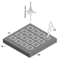
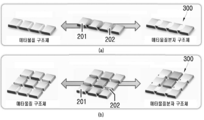
도 5는 본 발명의 일 실시예에 따른 메타물질 구조체가 하나의 메타물질분자 구조체로 연결된 것을 도시한 개념도이다.
도 6은 본 발명의 일 실시예에 따른 능동형 메타물질 어레이의 제조 방법을 설명하기 위한 순서도이다.
202: 전도도 가변 물질층 203: 전해질 물질층
204: 게이트 전극 210: 제 1 전해질 물질층
220: 제 2 전해질 물질층 211: 제1 게이트 전극
221: 제 2 게이트 전극 300: 메타물질분자 구조체
Claims (13)
- 능동형 메타물질 어레이에 있어서,
기판;
상기 기판 상에 서로 이격하여 배치된 복수의 메타물질 구조체;
상기 복수의 메타물질 구조체 사이에 형성되어 상기 메타물질 구조체들을 선택적으로 연결하는 전도도 가변 물질 층;
상기 메타물질 구조체와 상기 전도도 가변 물질 층 상에 형성되는 전해질 물질층; 및
상기 기판의 일단에 배치되어 상기 전해질 물질층의 일 영역과 접촉하는 게이트 전극을 포함하되,
상기 게이트 전극은,
상기 게이트 전극에 외부 전압이 인가될 경우, 상기 전해질 물질층에 포함된 이온의 이동을 제어하여 상기 전도도 가변 물질 층의 전도도를 가변시키는 것인 능동형 메타물질 어레이. - 제 1 항에 있어서,
상기 전도도 가변 물질 층의 전도도 변화에 따라 상기 복수의 메타물질 구조체는 일체로 연결되거나 분리됨으로써, 공진 주파수와 위상이 변화되는 것인 능동형 메타물질 어레이. - 제 2 항에 있어서,
상기 전도도가 미리 설정된 기준 이상을 넘는 경우,
상기 복수의 메타물질 구조체는 하나의 메타물질분자 구조체로 제어되는 것인 능동형 메타물질 어레이. - 제 3 항에 있어서,
상기 메타물질분자 구조체는 상기 복수의 메타물질 구조체가 가로, 세로 및 행렬 중 어느 하나의 방법으로 배치되어 연결되는 것인 능동형 메타물질 어레이. - 제 1 항에 있어서,
상기 전해질 물질층은 전해질 액체, 젤, 혹은 고체화된 전해질을 포함하는 능동형 메타물질 어레이. - 제 1 항에 있어서,
상기 게이트 전극은 복수 단위로 구성되되, 각각의 게이트 전극은 상기 기판의 일단과 타단에 형성되며,
상기 각 게이트 전극에 상이한 전압이 인가되는 것인 능동형 메타물질 어레이. - 제 6 항에 있어서,
상기 전해질 물질층은 복수 의 단위로 구성된 제 1 전해질 물질층 및 제 2 전해질 물질층을 포함하고,
상기 게이트 전극은 상기 기판의 일단과 타단에 각각 배치되는 제 1 게이트 전극 및 제 2 게이트 전극을 포함하되,
상기 제 1 전해질 물질층은 상기 제 1 게이트 전극과 연결되고, 상기 제 2 전해질 물질층은 상기 제 2 게이트 전극과 연결되는 것인 능동형 메타물질 어레이. - 제 7 항에 있어서,
상기 제 1 및 제 2 전해질 물질층은 복수 단위의 바(bar) 형상으로 형성되되, 교번하여 배치되는 것인 능동형 메타물질 어레이. - 제 1 항에 있어서,
상기 전도도 가변 물질 층은 상기 메타물질 구조체의 아래에 형성되어 상기 메타물질 구조체들을 선택적으로 연결하는 것인 능동형 메타물질 어레이. - 제 1 항에 있어서,
상기 메타물질 구조체는 사각형으로 형성된 중간부와 상기 중간부의 양측에 형성되는 양단부로 구성되되,
상기 중간부의 가로의 길이는 상기 양단부의 가로의 길이 보다 길고, 상기 중간부의 세로의 길이는 상기 양단부의 세로의 길이 보다 작게 형성되는 것인 능동형 메타물질 어레이. - 제 1 항에 있어서,
상기 전도도 가변 물질 층은 상기 복수의 메타물질 구조체들을 연결할 수 있는 길이로 형성되되, 일 방향에 대하여 복수 단위로 형성되고,
상기 복수 단위의 전도도 가변 물질 층은 서로 이격하여 배치되는 것인 능동형 메타물질 어레이. - 제 1 항에 있어서,
상기 전해질 물질층은 상기 전체의 메타물질 구조체의 크기에 대응하는 크기로 일체로 형성되거나 행렬 구조로 배열된 상기 메타물질 구조체의 각 열이나 각 행들의 길이에 대응하도록 복수 단위로 형성되는 것인 능동형 메타물질 어레이. - 능동형 메타물질 어레이의 제조 방법에 있어서,
기판 상에 서로 이격하여 배치되도록 복수의 메타물질 구조체를 형성하는 단계;
상기 복수의 메타물질 구조체 사이에 상기 메타물질 구조체들을 선택적으로 연결하도록 전도도 가변 물질 층을 형성하는 단계;
상기 메타물질 구조체와 상기 전도도 가변 물질 층 상에 전해질 물질층을 형성하는 단계; 및
상기 기판의 일단에 상기 전해질 물질층의 일 영역과 접촉하도록 게이트 전극을 형성하는 단계를 포함하되,
상기 전해질 물질층은 게이트 전극에 외부 전압이 인가될 경우, 상기 전해질 물질층 포함된 이온의 이동을 제어하여 상기 전도도 가변 물질 층의 전도도를 가변시키는 것인 능동형 메타물질 어레이의 제조 방법.
Priority Applications (2)
| Application Number | Priority Date | Filing Date | Title |
|---|---|---|---|
| PCT/KR2017/001929 WO2017164523A1 (ko) | 2016-03-25 | 2017-02-22 | 능동형 메타물질 어레이 및 그 제조 방법 |
| US16/087,701 US11520206B2 (en) | 2016-03-25 | 2017-02-22 | Active metamaterial array and method for manufacturing the same |
Applications Claiming Priority (2)
| Application Number | Priority Date | Filing Date | Title |
|---|---|---|---|
| KR1020160036044 | 2016-03-25 | ||
| KR20160036044 | 2016-03-25 |
Publications (2)
| Publication Number | Publication Date |
|---|---|
| KR20170112935A true KR20170112935A (ko) | 2017-10-12 |
| KR101785508B1 KR101785508B1 (ko) | 2017-10-17 |
Family
ID=60140602
Family Applications (2)
| Application Number | Title | Priority Date | Filing Date |
|---|---|---|---|
| KR1020160132263A Expired - Fee Related KR101785508B1 (ko) | 2016-03-25 | 2016-10-12 | 능동형 메타물질 어레이 및 그 제조 방법 |
| KR1020170038565A Expired - Fee Related KR101922572B1 (ko) | 2016-03-25 | 2017-03-27 | 이온성 젤 미세 패턴 형성 방법 |
Family Applications After (1)
| Application Number | Title | Priority Date | Filing Date |
|---|---|---|---|
| KR1020170038565A Expired - Fee Related KR101922572B1 (ko) | 2016-03-25 | 2017-03-27 | 이온성 젤 미세 패턴 형성 방법 |
Country Status (2)
| Country | Link |
|---|---|
| US (1) | US11520206B2 (ko) |
| KR (2) | KR101785508B1 (ko) |
Cited By (2)
| Publication number | Priority date | Publication date | Assignee | Title |
|---|---|---|---|---|
| KR101888175B1 (ko) * | 2017-07-21 | 2018-08-14 | 삼육대학교산학협력단 | 외곽 사각고리 추가형 테라헤르츠 능동공진기 |
| US11456539B2 (en) * | 2018-07-27 | 2022-09-27 | Kuang-Chi Cutting Edge Technology Ltd. | Absorbing metamaterial |
Families Citing this family (3)
| Publication number | Priority date | Publication date | Assignee | Title |
|---|---|---|---|---|
| KR102630085B1 (ko) | 2018-05-30 | 2024-01-25 | 한양대학교 산학협력단 | 초미세 패턴 및 그 제조 방법 |
| CN109814283B (zh) * | 2019-03-27 | 2020-08-28 | 电子科技大学 | 低电压驱动的常开型太赫兹超表面调制器及制备方法 |
| CN119278549A (zh) * | 2022-05-31 | 2025-01-07 | 富士胶片株式会社 | 电磁波控制元件及其制造方法 |
Family Cites Families (10)
| Publication number | Priority date | Publication date | Assignee | Title |
|---|---|---|---|---|
| KR100690929B1 (ko) * | 2006-05-03 | 2007-03-09 | 한국기계연구원 | 건식필름레지스트를 이용하여 원하는 패턴두께 또는 높은종횡비를 가지는 고해상도패턴 형성 방법 |
| US7741933B2 (en) | 2006-06-30 | 2010-06-22 | The Charles Stark Draper Laboratory, Inc. | Electromagnetic composite metamaterial |
| WO2008121159A2 (en) | 2006-10-19 | 2008-10-09 | Los Alamos National Security Llc | Active terahertz metamaterial devices |
| WO2008097300A2 (en) | 2007-02-08 | 2008-08-14 | Regents Of The University Of Minnesota | Ion gels and electronic devices utilizing ion gels |
| US9459375B2 (en) | 2010-11-05 | 2016-10-04 | Tufts University | Active manipulation of electromagnetic wave propagation in metamaterials |
| US9106342B2 (en) | 2011-05-03 | 2015-08-11 | William Marsh Rice University | Device and method for modulating transmission of terahertz waves |
| US8836446B2 (en) | 2012-06-21 | 2014-09-16 | University Of Notre Dame Du Lac | Methods and apparatus for terahertz wave amplitude modulation |
| US10468326B2 (en) | 2013-06-10 | 2019-11-05 | Purdue Research Foundation | Metamaterial systems and methods for their use |
| KR101626806B1 (ko) | 2014-07-25 | 2016-06-09 | 한국해양대학교 산학협력단 | 주파수 변조가 가능한 고효율 테라헤르츠 트랜스시버 |
| US20190058242A1 (en) * | 2017-08-21 | 2019-02-21 | Joseph Akwo Tabe | Energy harvesting substrate network and communication apparatus |
-
2016
- 2016-10-12 KR KR1020160132263A patent/KR101785508B1/ko not_active Expired - Fee Related
-
2017
- 2017-02-22 US US16/087,701 patent/US11520206B2/en active Active
- 2017-03-27 KR KR1020170038565A patent/KR101922572B1/ko not_active Expired - Fee Related
Cited By (2)
| Publication number | Priority date | Publication date | Assignee | Title |
|---|---|---|---|---|
| KR101888175B1 (ko) * | 2017-07-21 | 2018-08-14 | 삼육대학교산학협력단 | 외곽 사각고리 추가형 테라헤르츠 능동공진기 |
| US11456539B2 (en) * | 2018-07-27 | 2022-09-27 | Kuang-Chi Cutting Edge Technology Ltd. | Absorbing metamaterial |
Also Published As
| Publication number | Publication date |
|---|---|
| US11520206B2 (en) | 2022-12-06 |
| KR101785508B1 (ko) | 2017-10-17 |
| KR20170113285A (ko) | 2017-10-12 |
| KR101922572B1 (ko) | 2018-11-28 |
| US20200301224A1 (en) | 2020-09-24 |
Similar Documents
| Publication | Publication Date | Title |
|---|---|---|
| KR101785508B1 (ko) | 능동형 메타물질 어레이 및 그 제조 방법 | |
| US8674792B2 (en) | Tunable metamaterials | |
| CN110574236B (zh) | 一种液晶可重构多波束相控阵列 | |
| US5619365A (en) | Elecronically tunable optical periodic surface filters with an alterable resonant frequency | |
| CN1914766B (zh) | 可调装置 | |
| US8421706B2 (en) | Metamaterial microwave lens | |
| US8174341B2 (en) | Thin film based split resonator tunable metamaterial | |
| US11522128B2 (en) | Metasurface phase change communicator | |
| US8134521B2 (en) | Electronically tunable microwave reflector | |
| KR101647045B1 (ko) | 3차원 직립형 메타물질 구조물 및 그 제조방법 | |
| US20180241131A1 (en) | Optical surface-scattering elements and metasurfaces | |
| Luo et al. | An active metamaterial antenna with MEMS-modulated scanning radiation beams | |
| US20090096545A1 (en) | Dynamic frequency tuning of electric and magnetic metamaterial response | |
| TW201739107A (zh) | 具有微電氣機械系統調諧射頻共振器之天線及其製造方法 | |
| JP5325299B2 (ja) | 光変調のための調整可能なナノワイヤ共振空胴 | |
| US9734951B2 (en) | MEMS electrostatic actuator | |
| US11594795B2 (en) | Switchable element | |
| US20140125897A1 (en) | Electric device having variable capacitance element and its manufacture | |
| CN110582891A (zh) | 具有用于控制射束方向的变抗器的介电行波波导 | |
| US5627672A (en) | Controllable optical periodic surface filters as a Q-switch in a resonant cavity | |
| US7965250B2 (en) | Microwave lens | |
| CN119596573B (zh) | 一种电控太赫兹双频相位调制器 | |
| CN112909564A (zh) | 一种基于氧化钒相变的电触发可重构太赫兹数字超表面 | |
| EP2083431A1 (en) | Microelectromechanical system tunable capacitor | |
| CN120380663A (zh) | 一种可重构超表面及其控制方法、可重构天线及基站 |
Legal Events
| Date | Code | Title | Description |
|---|---|---|---|
| A201 | Request for examination | ||
| PA0109 | Patent application |
St.27 status event code: A-0-1-A10-A12-nap-PA0109 |
|
| PA0201 | Request for examination |
St.27 status event code: A-1-2-D10-D11-exm-PA0201 |
|
| E701 | Decision to grant or registration of patent right | ||
| PE0701 | Decision of registration |
St.27 status event code: A-1-2-D10-D22-exm-PE0701 |
|
| GRNT | Written decision to grant | ||
| PR0701 | Registration of establishment |
St.27 status event code: A-2-4-F10-F11-exm-PR0701 |
|
| PR1002 | Payment of registration fee |
St.27 status event code: A-2-2-U10-U11-oth-PR1002 Fee payment year number: 1 |
|
| PG1501 | Laying open of application |
St.27 status event code: A-1-1-Q10-Q12-nap-PG1501 |
|
| PG1601 | Publication of registration |
St.27 status event code: A-4-4-Q10-Q13-nap-PG1601 |
|
| PR1001 | Payment of annual fee |
St.27 status event code: A-4-4-U10-U11-oth-PR1001 Fee payment year number: 4 |
|
| PR1001 | Payment of annual fee |
St.27 status event code: A-4-4-U10-U11-oth-PR1001 Fee payment year number: 5 |
|
| PN2301 | Change of applicant |
St.27 status event code: A-5-5-R10-R13-asn-PN2301 St.27 status event code: A-5-5-R10-R11-asn-PN2301 |
|
| PR1001 | Payment of annual fee |
St.27 status event code: A-4-4-U10-U11-oth-PR1001 Fee payment year number: 6 |
|
| P22-X000 | Classification modified |
St.27 status event code: A-4-4-P10-P22-nap-X000 |
|
| P22-X000 | Classification modified |
St.27 status event code: A-4-4-P10-P22-nap-X000 |
|
| PC1903 | Unpaid annual fee |
St.27 status event code: A-4-4-U10-U13-oth-PC1903 Not in force date: 20230930 Payment event data comment text: Termination Category : DEFAULT_OF_REGISTRATION_FEE |
|
| PC1903 | Unpaid annual fee |
St.27 status event code: N-4-6-H10-H13-oth-PC1903 Ip right cessation event data comment text: Termination Category : DEFAULT_OF_REGISTRATION_FEE Not in force date: 20230930 |