KR20170112991A - 근거리 전자기파 흡수 필름 - Google Patents
근거리 전자기파 흡수 필름 Download PDFInfo
- Publication number
- KR20170112991A KR20170112991A KR1020160182492A KR20160182492A KR20170112991A KR 20170112991 A KR20170112991 A KR 20170112991A KR 1020160182492 A KR1020160182492 A KR 1020160182492A KR 20160182492 A KR20160182492 A KR 20160182492A KR 20170112991 A KR20170112991 A KR 20170112991A
- Authority
- KR
- South Korea
- Prior art keywords
- electromagnetic wave
- film
- thin metal
- wave absorbing
- metal film
- Prior art date
- Legal status (The legal status is an assumption and is not a legal conclusion. Google has not performed a legal analysis and makes no representation as to the accuracy of the status listed.)
- Abandoned
Links
Images









Classifications
-
- H—ELECTRICITY
- H01—ELECTRIC ELEMENTS
- H01Q—ANTENNAS, i.e. RADIO AERIALS
- H01Q17/00—Devices for absorbing waves radiated from an antenna; Combinations of such devices with active antenna elements or systems
- H01Q17/007—Devices for absorbing waves radiated from an antenna; Combinations of such devices with active antenna elements or systems with means for controlling the absorption
-
- H—ELECTRICITY
- H05—ELECTRIC TECHNIQUES NOT OTHERWISE PROVIDED FOR
- H05K—PRINTED CIRCUITS; CASINGS OR CONSTRUCTIONAL DETAILS OF ELECTRIC APPARATUS; MANUFACTURE OF ASSEMBLAGES OF ELECTRICAL COMPONENTS
- H05K9/00—Screening of apparatus or components against electric or magnetic fields
- H05K9/0073—Shielding materials
- H05K9/0081—Electromagnetic shielding materials, e.g. EMI, RFI shielding
- H05K9/0084—Electromagnetic shielding materials, e.g. EMI, RFI shielding comprising a single continuous metallic layer on an electrically insulating supporting structure, e.g. metal foil, film, plating coating, electro-deposition, vapour-deposition
-
- B—PERFORMING OPERATIONS; TRANSPORTING
- B32—LAYERED PRODUCTS
- B32B—LAYERED PRODUCTS, i.e. PRODUCTS BUILT-UP OF STRATA OF FLAT OR NON-FLAT, e.g. CELLULAR OR HONEYCOMB, FORM
- B32B15/00—Layered products comprising a layer of metal
- B32B15/04—Layered products comprising a layer of metal comprising metal as the main or only constituent of a layer, which is next to another layer of the same or of a different material
- B32B15/08—Layered products comprising a layer of metal comprising metal as the main or only constituent of a layer, which is next to another layer of the same or of a different material of synthetic resin
-
- B—PERFORMING OPERATIONS; TRANSPORTING
- B32—LAYERED PRODUCTS
- B32B—LAYERED PRODUCTS, i.e. PRODUCTS BUILT-UP OF STRATA OF FLAT OR NON-FLAT, e.g. CELLULAR OR HONEYCOMB, FORM
- B32B3/00—Layered products comprising a layer with external or internal discontinuities or unevennesses, or a layer of non-planar shape; Layered products comprising a layer having particular features of form
- B32B3/26—Layered products comprising a layer with external or internal discontinuities or unevennesses, or a layer of non-planar shape; Layered products comprising a layer having particular features of form characterised by a particular shape of the outline of the cross-section of a continuous layer; characterised by a layer with cavities or internal voids ; characterised by an apertured layer
- B32B3/266—Layered products comprising a layer with external or internal discontinuities or unevennesses, or a layer of non-planar shape; Layered products comprising a layer having particular features of form characterised by a particular shape of the outline of the cross-section of a continuous layer; characterised by a layer with cavities or internal voids ; characterised by an apertured layer characterised by an apertured layer, the apertures going through the whole thickness of the layer, e.g. expanded metal, perforated layer, slit layer regular cells B32B3/12
-
- B—PERFORMING OPERATIONS; TRANSPORTING
- B32—LAYERED PRODUCTS
- B32B—LAYERED PRODUCTS, i.e. PRODUCTS BUILT-UP OF STRATA OF FLAT OR NON-FLAT, e.g. CELLULAR OR HONEYCOMB, FORM
- B32B33/00—Layered products characterised by particular properties or particular surface features, e.g. particular surface coatings; Layered products designed for particular purposes not covered by another single class
-
- H—ELECTRICITY
- H01—ELECTRIC ELEMENTS
- H01Q—ANTENNAS, i.e. RADIO AERIALS
- H01Q17/00—Devices for absorbing waves radiated from an antenna; Combinations of such devices with active antenna elements or systems
-
- H—ELECTRICITY
- H05—ELECTRIC TECHNIQUES NOT OTHERWISE PROVIDED FOR
- H05K—PRINTED CIRCUITS; CASINGS OR CONSTRUCTIONAL DETAILS OF ELECTRIC APPARATUS; MANUFACTURE OF ASSEMBLAGES OF ELECTRICAL COMPONENTS
- H05K9/00—Screening of apparatus or components against electric or magnetic fields
- H05K9/0073—Shielding materials
- H05K9/0081—Electromagnetic shielding materials, e.g. EMI, RFI shielding
- H05K9/0086—Electromagnetic shielding materials, e.g. EMI, RFI shielding comprising a single discontinuous metallic layer on an electrically insulating supporting structure, e.g. metal grid, perforated metal foil, film, aggregated flakes, sintering
-
- H—ELECTRICITY
- H05—ELECTRIC TECHNIQUES NOT OTHERWISE PROVIDED FOR
- H05K—PRINTED CIRCUITS; CASINGS OR CONSTRUCTIONAL DETAILS OF ELECTRIC APPARATUS; MANUFACTURE OF ASSEMBLAGES OF ELECTRICAL COMPONENTS
- H05K9/00—Screening of apparatus or components against electric or magnetic fields
- H05K9/0073—Shielding materials
- H05K9/0094—Shielding materials being light-transmitting, e.g. transparent, translucent
- H05K9/0096—Shielding materials being light-transmitting, e.g. transparent, translucent for television displays, e.g. plasma display panel
-
- B—PERFORMING OPERATIONS; TRANSPORTING
- B32—LAYERED PRODUCTS
- B32B—LAYERED PRODUCTS, i.e. PRODUCTS BUILT-UP OF STRATA OF FLAT OR NON-FLAT, e.g. CELLULAR OR HONEYCOMB, FORM
- B32B2307/00—Properties of the layers or laminate
- B32B2307/20—Properties of the layers or laminate having particular electrical or magnetic properties, e.g. piezoelectric
- B32B2307/212—Electromagnetic interference shielding
Landscapes
- Engineering & Computer Science (AREA)
- Physics & Mathematics (AREA)
- Microelectronics & Electronic Packaging (AREA)
- Electromagnetism (AREA)
- Plasma & Fusion (AREA)
- Shielding Devices Or Components To Electric Or Magnetic Fields (AREA)
- Laminated Bodies (AREA)
Abstract
얇은 금속 필름은 표면 전체에 50 ㎛ 이하의 간격들로 200 ㎛ 이하의 직경의 레이저 빔 보어 가공된 홀들, 그리고 표면에 부분적으로 투과 가시성을 주는 크기의 복수의 개구들을 갖는다.
Description
도 1b는 도 1a의 라인 A-A 을 따라 취해진 횡단면도이다.
도 1c는 도 1a의 부분 확대도이다.
도 2는 본 발명의 근거리 전자기파 흡수 필름을 형성하기 위한 미세한 레이저 빔 보어 가공된 홀들의 배열들의 다른 실시예를 도시하는 부분 확대 평면도이다.
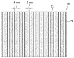
도 3은 본 발명의 근거리 전자기파 흡수 필름을 형성하기 위한 개구들의 배열들의 실시예를 도시하는 평면도이다.
도 4는 본 발명의 근거리 전자기파 흡수 필름을 형성하기 위한 개구의 배열들의 다른 실시예를 도시하는 평면도이다.
도 5는 본 발명의 근거리 전자기파 흡수 필름을 형성하기 위한 개구들의 배열들의 다른 실시예를 도시하는 평면도이다.
도 6은 본 발명의 근거리 전자기파 흡수 필름을 형성하기 위한 개구들의 배열들의 또 다른 실시예를 도시하는 평면도이다.
도 7은 본 발명의 근거리 전자기파 흡수 필름을 형성하기 위한 개구들의 배열들의 또 다른 실시예를 도시하는 평면도이다.
도 8은 본 발명의 근거리 전자기파 흡수 필름을 형성하기 위한 개구들의 배열들의 또 다른 실시예를 도시하는 평면도이다.
도 9는 본 발명의 근거리 전자기파 흡수 필름을 형성하기 위한 개구들의 배열들의 또 다른 실시예를 도시하는 평면도이다.
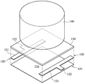
도 10a는 근거리 전자기파 흡수 필름의 전기 저항을 측정하기 위한 기기를 도시하는 사시도이다.
도 10b는 도 10a의 기기에 의한 근거리 전자기파 흡수 필름의 전기 저항의 측정을 도시하는 평면도이다.
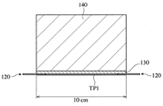
도 10c는 도 10b의 라인 B-B 을 따라 취해진 횡단면도이다.
도 11a는 근거리 전자기파 흡수 필름의 전자기파 흡수 능력을 평가하기 위한 시스템을 도시하는 평면도이다.
도 11b는 근거리 전자기파 흡수 필름의 전자기파 흡수 능력을 평가하기 위한 시스템을 도시하는 부분 횡단 정면도이다.
도 12는 기준예(Reference Example) 1 의 보어 가공된 복합 필름을 도시하는 현미경 사진(photomicrograph)이다.
도 13은 비교예 1 의 보어 가공된 복합 필름을 도시하는 현미경 사진이다.
도 14는 비교예 2 의 보어 가공된 복합 필름을 도시하는 현미경 사진이다.
도 15는 기준예 1 그리고 비교예 1 및 2 의 보어 가공된 복합 필름들의 입사(incident) 전자기파들의 주파수와 S11 사이의 관계들을 도시하는 그래프이다.
도 16은 기준예 1 그리고 비교예 1 및 2 의 보어 가공된 복합 필름들의 입사 전자기파들의 주파수와 투과 감쇠 파워 비(Rtp) 사이의 관계들을 도시하는 그래프이다.
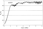
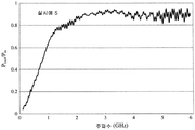
도 17은 0.1 내지 6 ㎓ 에서 기준예 1 의 근거리 전자기파 흡수 필름의 Ploss/Pin 을 도시하는 그래프이다.
도 18은 기준예 2 의 보어 가공된 복합 필름을 도시하는 현미경 사진이다.
도 19는 0.1 내지 6 ㎓ 에서 기준예 2 의 보어 가공된 복합 필름의 Ploss/Pin 을 도시하는 그래프이다.
도 20은 0.1 내지 6 ㎓ 에서 실시예 1 의 근거리 전자기파 흡수 필름의 S11, S21 및 Rtp 를 도시하는 그래프이다.
도 21은 0.1 내지 6 ㎓ 에서 실시예 1 의 근거리 전자기파 흡수 필름의 Ploss/Pin 을 도시하는 그래프이다.
도 22는 0.1 내지 6 ㎓ 에서 실시예 2 의 근거리 전자기파 흡수 필름의 S11, S21 및 Rtp 를 도시하는 그래프이다.
도 23은 0.1 내지 6 ㎓ 에서 실시예 2 의 근거리 전자기파 흡수 필름의 Ploss/Pin 을 도시하는 그래프이다.
도 24는 0.1 내지 6 ㎓ 에서 실시예 3 의 근거리 전자기파 흡수 필름의 S11, S21 및 Rtp 를 도시하는 그래프이다.
도 25는 0.1 내지 6 ㎓ 에서 실시예 3 의 근거리 전자기파 흡수 필름의 Ploss/Pin 을 도시하는 그래프이다.
도 26은 0.1 내지 6 ㎓ 에서 실시예 4 의 근거리 전자기파 흡수 필름의 S11, S21 및 Rtp 를 도시하는 그래프이다.
도 27은 0.1 내지 6 ㎓ 에서 실시예 4 의 근거리 전자기파 흡수 필름의 Ploss/Pin 을 도시하는 그래프이다.
도 28은 0.1 내지 6 ㎓ 에서 실시예 5 의 근거리 전자기파 흡수 필름의 S11, S21 및 Rtp 를 도시하는 그래프이다.
도 29는 0.1 내지 6 ㎓ 에서 실시예 5 의 근거리 전자기파 흡수 필름의 Ploss/Pin 을 도시하는 그래프이다.
| 번호 | 기준예 1 | 비교예 1 | 비교예 2 |
| 대응 도면 | 도 12 | 도 13 | 도 14 |
| 교차 각도 θ(1)(°) | 90 | 90 | 90 |
| 최대 폭 Wmax(㎛) | 15 | 60 | 0 |
| 평균 폭Wav(㎛) | 7 | 50 | 0 |
| 전기 저항 (Ω/100㎠) | 60 | 6 | ∞ |
| 번호 | 실시예 1 | 실시예 2 | 실시예 3 | 실시예 4 | 실시예 5 |
| 얇은 금속 필름 금속(두께 : ㎚) |
기준예 1 Ni(50) |
기준예 2 Al(80) |
기준예 2 Al(80) |
기준예 2 Al(80) |
기준예 2 Al(80) |
| 보어 가공된 얇은 금속 필름 | 도 12 | 도 18 | 도 18 | 도 18 | 도 18 |
| 개구들 | 도 3 | 도 4 | 도 5 | 도 6 | 도 9 |
| 개구들의 면적비(%) | 33 | 24 | 36 | 40 | 44 |
10 : 플라스틱 필름
11 : 얇은 금속 필름
11a : 남아있는 얇은 금속 필름 부분
12 : 레이저 빔 보어 가공된 홀
12a, 12b : 레이저 빔 보어 가공된 홀들의 라인
13 : 주요 나머지 부분
14 : 브리지형 부분
20 : 근거리 전자기파 흡수 필름
21 : 개구
22 : 개구 후 남아있는 부분
120 : 전극
121 : 전극 본체 부분
122 : 전극 연장부
130 : 투명 아크릴 플레이트
140 : 원통형 추
220 : 절연 기재
221 : 접지된 전극
222 : 전도성 핀
223 : 동축 케이블
D : 레이저 빔 보어 가공된 홀의 직경
W : 브리지형 부분의 폭
T : 인접한 레이저 빔 보어 가공된 홀들의 라인들 사이의 중심선 거리
TP1, TP2 : 근거리 전자기파 흡수 필름의 시편
MSL : 마이크로스트립라인
NA : 네트워크 분석기
Claims (8)
- 플라스틱 필름, 그리고 상기 플라스틱 필름의 일 표면에 형성되는 단일 층 또는 다중 층의 얇은 금속 필름을 포함하는 근거리 전자기파 흡수 필름(near-field electromagnetic wave absorbing film)으로서,
상기 얇은 금속 필름은 상기 표면 전체에 50 ㎛ 이하의 간격들로 200 ㎛ 이하의 직경의 레이저 빔 보어 가공된 홀(laser-beam-bored hole)들, 및 상기 표면에 부분적으로 투과 가시성(transmission viewability)을 주는 크기의 복수의 개구들을 갖는, 근거리 전자기파 흡수 필름. - 제 1 항에 있어서,
상기 레이저 빔 보어 가공된 홀들은 100 ㎛ 이하의 직경들을 갖는, 근거리 전자기파 흡수 필름. - 제 2 항에 있어서,
상기 레이저 빔 보어 가공된 홀들은 20 내지 100 ㎛ 의 직경들을 갖는, 근거리 전자기파 흡수 필름. - 제 1 항에 있어서,
상기 레이저 빔 보어 가공된 홀들은 20 ㎛ 이하의 간격들로 배열되는, 근거리 전자기파 흡수 필름. - 제 1 항에 있어서,
상기 얇은 금속 필름에 형성되는 상기 개구들은 적어도 2 개의 방향들로 배열되는, 근거리 전자기파 흡수 필름. - 제 1 항에 있어서,
상기 개구들의 면적비(area ratio)는 15 내지 60 % 인, 근거리 전자기파 흡수 필름. - 제 1 항에 있어서,
상기 얇은 금속 필름의 두께는 10 내지 300 ㎚ 인, 근거리 전자기파 흡수 필름. - 제 1 항 내지 제 7 항 중 어느 한 항에 있어서,
상기 얇은 금속 필름은 알루미늄, 구리, 은, 주석, 니켈, 코발트, 크롬 및 이들의 합금들로 이루어지는 그룹으로부터 선택되는 적어도 하나의 금속으로 만들어지는, 근거리 전자기파 흡수 필름.
Applications Claiming Priority (2)
| Application Number | Priority Date | Filing Date | Title |
|---|---|---|---|
| JP2016074369A JP6027281B1 (ja) | 2016-04-01 | 2016-04-01 | 近傍界電磁波吸収フィルム |
| JPJP-P-2016-074369 | 2016-04-01 |
Publications (1)
| Publication Number | Publication Date |
|---|---|
| KR20170112991A true KR20170112991A (ko) | 2017-10-12 |
Family
ID=57326668
Family Applications (1)
| Application Number | Title | Priority Date | Filing Date |
|---|---|---|---|
| KR1020160182492A Abandoned KR20170112991A (ko) | 2016-04-01 | 2016-12-29 | 근거리 전자기파 흡수 필름 |
Country Status (6)
| Country | Link |
|---|---|
| US (1) | US10056697B2 (ko) |
| EP (1) | EP3226668B1 (ko) |
| JP (1) | JP6027281B1 (ko) |
| KR (1) | KR20170112991A (ko) |
| CN (1) | CN107263936B (ko) |
| TW (1) | TWI706713B (ko) |
Families Citing this family (8)
| Publication number | Priority date | Publication date | Assignee | Title |
|---|---|---|---|---|
| DE102016101756B4 (de) * | 2016-02-01 | 2026-04-02 | Vega Grieshaber Kg | Verfahren zur Bestimmung und Anzeige der optimalen Materialstärke bei der Füllstandmessung mit Radarsensoren |
| JP6461414B1 (ja) * | 2018-08-02 | 2019-01-30 | 清二 加川 | 電磁波吸収複合シート |
| US11281340B2 (en) * | 2019-01-18 | 2022-03-22 | Cirque Corporation | Radio frequency transparent capacitive touch systems and methods |
| JP7363103B2 (ja) | 2019-05-30 | 2023-10-18 | 東洋インキScホールディングス株式会社 | 電磁波シールドシートおよびプリント配線板 |
| KR102809586B1 (ko) * | 2021-08-27 | 2025-05-22 | 삼성전자주식회사 | 조리기기 외장재 및 그 제조방법 |
| WO2023027305A1 (ko) | 2021-08-27 | 2023-03-02 | 삼성전자주식회사 | 조리기기용 외장재 및 그 제조방법 |
| JP7323692B1 (ja) * | 2022-08-19 | 2023-08-08 | 清二 加川 | 近傍界電磁波吸収体 |
| JPWO2024185241A1 (ko) * | 2023-03-07 | 2024-09-12 |
Family Cites Families (16)
| Publication number | Priority date | Publication date | Assignee | Title |
|---|---|---|---|---|
| IT214086Z2 (it) | 1988-03-03 | 1990-04-02 | Salvarani Ind Spa | Modulo di cucina componibile |
| US5855988A (en) | 1995-11-27 | 1999-01-05 | Nippon Paint Co., Ltd. | Electromagnetic wave absorbing shielding material |
| JPH09148782A (ja) | 1995-11-27 | 1997-06-06 | Nippon Paint Co Ltd | 透明電磁波吸収シールド材 |
| JP2002313140A (ja) * | 2001-04-13 | 2002-10-25 | Mitsui Chemicals Inc | 透明導電性フィルム及び光学フィルター並びにその製造方法 |
| JP2002317280A (ja) * | 2001-04-18 | 2002-10-31 | Toyo Metallizing Co Ltd | 金属化プラスチックフィルム |
| KR100939747B1 (ko) * | 2001-05-16 | 2010-02-04 | 가부시키가이샤 브리지스톤 | 전자파 실드성 광투과 창재, 그 제조 방법 및 표시 패널 |
| EP1993338A4 (en) * | 2006-03-09 | 2011-05-25 | Bridgestone Corp | PROCESS FOR MANUFACTURING TRANSLUCENT ELECTROMAGNETIC WAVE PROTECTION MATERIALS, TRANSLUCENT ELECTROMAGNETIC WAVE PROTECTIVE MATERIALS, AND DISPLAY FILTER |
| KR20090108781A (ko) * | 2008-04-14 | 2009-10-19 | 주식회사 동진쎄미켐 | 흑색 도전성 페이스트 조성물, 이를 포함하는 전자파차폐용 필터 및 표시 장치 |
| US9238351B2 (en) | 2009-02-13 | 2016-01-19 | Seiji Kagawa | Composite film of linearly-scratched, thin metal film and plastic film, and its production apparatus |
| KR20120039042A (ko) * | 2009-08-03 | 2012-04-24 | 쓰리엠 이노베이티브 프로퍼티즈 컴파니 | 광학적으로 투명한 전도성 금속 또는 금속 합금 박막의 형성 방법 및 그에 의해 제조된 필름 |
| JP2011142198A (ja) * | 2010-01-07 | 2011-07-21 | Mitsubishi Rayon Co Ltd | 電波吸収体 |
| TWI435205B (zh) * | 2011-05-12 | 2014-04-21 | Subtron Technology Co Ltd | 蓋板結構及其製作方法 |
| JP5069365B1 (ja) * | 2011-06-30 | 2012-11-07 | 清二 加川 | 近傍界ノイズ抑制フィルム |
| EP2787803B1 (en) * | 2011-11-30 | 2017-06-28 | Seiji Kagawa | Electromagnetic wave absorbing composite sheet |
| WO2014126394A1 (ko) * | 2013-02-15 | 2014-08-21 | 주식회사 아모텍 | 전자파 흡수시트 및 이를 구비하는 안테나 모듈 |
| WO2014148589A1 (ja) * | 2013-03-21 | 2014-09-25 | 株式会社ノリタケカンパニーリミテド | 電磁波シールド板 |
-
2016
- 2016-04-01 JP JP2016074369A patent/JP6027281B1/ja not_active Expired - Fee Related
- 2016-11-24 EP EP16200503.7A patent/EP3226668B1/en active Active
- 2016-11-28 TW TW105139019A patent/TWI706713B/zh active
- 2016-11-29 US US15/363,793 patent/US10056697B2/en active Active
- 2016-12-29 KR KR1020160182492A patent/KR20170112991A/ko not_active Abandoned
-
2017
- 2017-01-18 CN CN201710040228.7A patent/CN107263936B/zh active Active
Also Published As
| Publication number | Publication date |
|---|---|
| CN107263936B (zh) | 2021-04-09 |
| EP3226668B1 (en) | 2021-05-05 |
| TWI706713B (zh) | 2020-10-01 |
| US20170288314A1 (en) | 2017-10-05 |
| JP6027281B1 (ja) | 2016-11-16 |
| JP2017188506A (ja) | 2017-10-12 |
| CN107263936A (zh) | 2017-10-20 |
| EP3226668A1 (en) | 2017-10-04 |
| US10056697B2 (en) | 2018-08-21 |
| TW201811157A (zh) | 2018-03-16 |
Similar Documents
| Publication | Publication Date | Title |
|---|---|---|
| KR20170112991A (ko) | 근거리 전자기파 흡수 필름 | |
| JP4685977B2 (ja) | 線状痕付き金属薄膜−プラスチック複合フィルム及びその製造装置 | |
| KR101725470B1 (ko) | 복합 전자파 흡수 필름 | |
| CN103959927A (zh) | 复合电磁波吸收片 | |
| JP5302287B2 (ja) | 電磁波吸収体 | |
| JP5214541B2 (ja) | 可視光透過性電磁波吸収フィルム及びそれを用いた可視光透過性電磁波吸収体 | |
| KR102168863B1 (ko) | 전자파 흡수 복합 시트 | |
| JP2010278090A (ja) | 電磁波吸収フィルム | |
| KR102482857B1 (ko) | 근거리 전자기파 흡수 필름 | |
| JP2012015381A (ja) | 電磁波吸収体及びそれを用いた内装材 | |
| KR20240026104A (ko) | 근방계 전자파 흡수체 | |
| JP5186535B2 (ja) | 透明電磁波吸収フィルム | |
| KR20250063350A (ko) | 더블 레이어 메타 물질 전자기파 흡수 장치 |
Legal Events
| Date | Code | Title | Description |
|---|---|---|---|
| PA0109 | Patent application |
St.27 status event code: A-0-1-A10-A12-nap-PA0109 |
|
| PG1501 | Laying open of application |
St.27 status event code: A-1-1-Q10-Q12-nap-PG1501 |
|
| A201 | Request for examination | ||
| PA0201 | Request for examination |
St.27 status event code: A-1-2-D10-D11-exm-PA0201 |
|
| E902 | Notification of reason for refusal | ||
| PE0902 | Notice of grounds for rejection |
St.27 status event code: A-1-2-D10-D21-exm-PE0902 |
|
| P11-X000 | Amendment of application requested |
St.27 status event code: A-2-2-P10-P11-nap-X000 |
|
| P13-X000 | Application amended |
St.27 status event code: A-2-2-P10-P13-nap-X000 |
|
| E701 | Decision to grant or registration of patent right | ||
| PE0701 | Decision of registration |
St.27 status event code: A-1-2-D10-D22-exm-PE0701 |
|
| PC1904 | Unpaid initial registration fee |
St.27 status event code: A-2-2-U10-U13-oth-PC1904 St.27 status event code: N-2-6-B10-B12-nap-PC1904 |