KR20170114976A - 투영 노광 방법 및 투영 노광 장치 - Google Patents
투영 노광 방법 및 투영 노광 장치 Download PDFInfo
- Publication number
- KR20170114976A KR20170114976A KR1020170043741A KR20170043741A KR20170114976A KR 20170114976 A KR20170114976 A KR 20170114976A KR 1020170043741 A KR1020170043741 A KR 1020170043741A KR 20170043741 A KR20170043741 A KR 20170043741A KR 20170114976 A KR20170114976 A KR 20170114976A
- Authority
- KR
- South Korea
- Prior art keywords
- mask
- substrate
- rotation
- image
- projection lens
- Prior art date
- Legal status (The legal status is an assumption and is not a legal conclusion. Google has not performed a legal analysis and makes no representation as to the accuracy of the status listed.)
- Granted
Links
Images


Classifications
-
- G—PHYSICS
- G03—PHOTOGRAPHY; CINEMATOGRAPHY; ANALOGOUS TECHNIQUES USING WAVES OTHER THAN OPTICAL WAVES; ELECTROGRAPHY; HOLOGRAPHY
- G03F—PHOTOMECHANICAL PRODUCTION OF TEXTURED OR PATTERNED SURFACES, e.g. FOR PRINTING, FOR PROCESSING OF SEMICONDUCTOR DEVICES; MATERIALS THEREFOR; ORIGINALS THEREFOR; APPARATUS SPECIALLY ADAPTED THEREFOR
- G03F7/00—Photomechanical, e.g. photolithographic, production of textured or patterned surfaces, e.g. printing surfaces; Materials therefor, e.g. comprising photoresists; Apparatus specially adapted therefor
- G03F7/70—Microphotolithographic exposure; Apparatus therefor
- G03F7/70691—Handling of masks or workpieces
- G03F7/70775—Position control, e.g. interferometers or encoders for determining the stage position
-
- G—PHYSICS
- G02—OPTICS
- G02B—OPTICAL ELEMENTS, SYSTEMS OR APPARATUS
- G02B13/00—Optical objectives specially designed for the purposes specified below
- G02B13/08—Anamorphotic objectives
-
- G—PHYSICS
- G03—PHOTOGRAPHY; CINEMATOGRAPHY; ANALOGOUS TECHNIQUES USING WAVES OTHER THAN OPTICAL WAVES; ELECTROGRAPHY; HOLOGRAPHY
- G03F—PHOTOMECHANICAL PRODUCTION OF TEXTURED OR PATTERNED SURFACES, e.g. FOR PRINTING, FOR PROCESSING OF SEMICONDUCTOR DEVICES; MATERIALS THEREFOR; ORIGINALS THEREFOR; APPARATUS SPECIALLY ADAPTED THEREFOR
- G03F7/00—Photomechanical, e.g. photolithographic, production of textured or patterned surfaces, e.g. printing surfaces; Materials therefor, e.g. comprising photoresists; Apparatus specially adapted therefor
- G03F7/20—Exposure; Apparatus therefor
- G03F7/2022—Multi-step exposure, e.g. hybrid; backside exposure; blanket exposure, e.g. for image reversal; edge exposure, e.g. for edge bead removal; corrective exposure
-
- G—PHYSICS
- G03—PHOTOGRAPHY; CINEMATOGRAPHY; ANALOGOUS TECHNIQUES USING WAVES OTHER THAN OPTICAL WAVES; ELECTROGRAPHY; HOLOGRAPHY
- G03F—PHOTOMECHANICAL PRODUCTION OF TEXTURED OR PATTERNED SURFACES, e.g. FOR PRINTING, FOR PROCESSING OF SEMICONDUCTOR DEVICES; MATERIALS THEREFOR; ORIGINALS THEREFOR; APPARATUS SPECIALLY ADAPTED THEREFOR
- G03F7/00—Photomechanical, e.g. photolithographic, production of textured or patterned surfaces, e.g. printing surfaces; Materials therefor, e.g. comprising photoresists; Apparatus specially adapted therefor
- G03F7/20—Exposure; Apparatus therefor
- G03F7/2002—Exposure; Apparatus therefor with visible light or UV light, through an original having an opaque pattern on a transparent support, e.g. film printing, projection printing; by reflection of visible or UV light from an original such as a printed image
- G03F7/2004—Exposure; Apparatus therefor with visible light or UV light, through an original having an opaque pattern on a transparent support, e.g. film printing, projection printing; by reflection of visible or UV light from an original such as a printed image characterised by the use of a particular light source, e.g. fluorescent lamps or deep UV light
-
- G—PHYSICS
- G03—PHOTOGRAPHY; CINEMATOGRAPHY; ANALOGOUS TECHNIQUES USING WAVES OTHER THAN OPTICAL WAVES; ELECTROGRAPHY; HOLOGRAPHY
- G03F—PHOTOMECHANICAL PRODUCTION OF TEXTURED OR PATTERNED SURFACES, e.g. FOR PRINTING, FOR PROCESSING OF SEMICONDUCTOR DEVICES; MATERIALS THEREFOR; ORIGINALS THEREFOR; APPARATUS SPECIALLY ADAPTED THEREFOR
- G03F7/00—Photomechanical, e.g. photolithographic, production of textured or patterned surfaces, e.g. printing surfaces; Materials therefor, e.g. comprising photoresists; Apparatus specially adapted therefor
- G03F7/20—Exposure; Apparatus therefor
- G03F7/2002—Exposure; Apparatus therefor with visible light or UV light, through an original having an opaque pattern on a transparent support, e.g. film printing, projection printing; by reflection of visible or UV light from an original such as a printed image
- G03F7/201—Exposure; Apparatus therefor with visible light or UV light, through an original having an opaque pattern on a transparent support, e.g. film printing, projection printing; by reflection of visible or UV light from an original such as a printed image characterised by an oblique exposure; characterised by the use of plural sources; characterised by the rotation of the optical device; characterised by a relative movement of the optical device, the light source, the sensitive system or the mask
-
- G—PHYSICS
- G03—PHOTOGRAPHY; CINEMATOGRAPHY; ANALOGOUS TECHNIQUES USING WAVES OTHER THAN OPTICAL WAVES; ELECTROGRAPHY; HOLOGRAPHY
- G03F—PHOTOMECHANICAL PRODUCTION OF TEXTURED OR PATTERNED SURFACES, e.g. FOR PRINTING, FOR PROCESSING OF SEMICONDUCTOR DEVICES; MATERIALS THEREFOR; ORIGINALS THEREFOR; APPARATUS SPECIALLY ADAPTED THEREFOR
- G03F7/00—Photomechanical, e.g. photolithographic, production of textured or patterned surfaces, e.g. printing surfaces; Materials therefor, e.g. comprising photoresists; Apparatus specially adapted therefor
- G03F7/70—Microphotolithographic exposure; Apparatus therefor
- G03F7/70216—Mask projection systems
- G03F7/70233—Optical aspects of catoptric systems, i.e. comprising only reflective elements, e.g. extreme ultraviolet [EUV] projection systems
-
- G—PHYSICS
- G03—PHOTOGRAPHY; CINEMATOGRAPHY; ANALOGOUS TECHNIQUES USING WAVES OTHER THAN OPTICAL WAVES; ELECTROGRAPHY; HOLOGRAPHY
- G03F—PHOTOMECHANICAL PRODUCTION OF TEXTURED OR PATTERNED SURFACES, e.g. FOR PRINTING, FOR PROCESSING OF SEMICONDUCTOR DEVICES; MATERIALS THEREFOR; ORIGINALS THEREFOR; APPARATUS SPECIALLY ADAPTED THEREFOR
- G03F7/00—Photomechanical, e.g. photolithographic, production of textured or patterned surfaces, e.g. printing surfaces; Materials therefor, e.g. comprising photoresists; Apparatus specially adapted therefor
- G03F7/70—Microphotolithographic exposure; Apparatus therefor
- G03F7/70216—Mask projection systems
- G03F7/70258—Projection system adjustments, e.g. adjustments during exposure or alignment during assembly of projection system
-
- G—PHYSICS
- G03—PHOTOGRAPHY; CINEMATOGRAPHY; ANALOGOUS TECHNIQUES USING WAVES OTHER THAN OPTICAL WAVES; ELECTROGRAPHY; HOLOGRAPHY
- G03F—PHOTOMECHANICAL PRODUCTION OF TEXTURED OR PATTERNED SURFACES, e.g. FOR PRINTING, FOR PROCESSING OF SEMICONDUCTOR DEVICES; MATERIALS THEREFOR; ORIGINALS THEREFOR; APPARATUS SPECIALLY ADAPTED THEREFOR
- G03F7/00—Photomechanical, e.g. photolithographic, production of textured or patterned surfaces, e.g. printing surfaces; Materials therefor, e.g. comprising photoresists; Apparatus specially adapted therefor
- G03F7/70—Microphotolithographic exposure; Apparatus therefor
- G03F7/70216—Mask projection systems
- G03F7/70275—Multiple projection paths, e.g. array of projection systems, microlens projection systems or tandem projection systems
-
- G—PHYSICS
- G03—PHOTOGRAPHY; CINEMATOGRAPHY; ANALOGOUS TECHNIQUES USING WAVES OTHER THAN OPTICAL WAVES; ELECTROGRAPHY; HOLOGRAPHY
- G03F—PHOTOMECHANICAL PRODUCTION OF TEXTURED OR PATTERNED SURFACES, e.g. FOR PRINTING, FOR PROCESSING OF SEMICONDUCTOR DEVICES; MATERIALS THEREFOR; ORIGINALS THEREFOR; APPARATUS SPECIALLY ADAPTED THEREFOR
- G03F7/00—Photomechanical, e.g. photolithographic, production of textured or patterned surfaces, e.g. printing surfaces; Materials therefor, e.g. comprising photoresists; Apparatus specially adapted therefor
- G03F7/70—Microphotolithographic exposure; Apparatus therefor
- G03F7/70216—Mask projection systems
- G03F7/70358—Scanning exposure, i.e. relative movement of patterned beam and workpiece during imaging
- G03F7/70366—Rotary scanning
-
- G—PHYSICS
- G03—PHOTOGRAPHY; CINEMATOGRAPHY; ANALOGOUS TECHNIQUES USING WAVES OTHER THAN OPTICAL WAVES; ELECTROGRAPHY; HOLOGRAPHY
- G03F—PHOTOMECHANICAL PRODUCTION OF TEXTURED OR PATTERNED SURFACES, e.g. FOR PRINTING, FOR PROCESSING OF SEMICONDUCTOR DEVICES; MATERIALS THEREFOR; ORIGINALS THEREFOR; APPARATUS SPECIALLY ADAPTED THEREFOR
- G03F7/00—Photomechanical, e.g. photolithographic, production of textured or patterned surfaces, e.g. printing surfaces; Materials therefor, e.g. comprising photoresists; Apparatus specially adapted therefor
- G03F7/70—Microphotolithographic exposure; Apparatus therefor
- G03F7/70483—Information management; Active and passive control; Testing; Wafer monitoring, e.g. pattern monitoring
- G03F7/70491—Information management, e.g. software; Active and passive control, e.g. details of controlling exposure processes or exposure tool monitoring processes
- G03F7/70525—Controlling normal operating mode, e.g. matching different apparatus, remote control or prediction of failure
-
- G—PHYSICS
- G03—PHOTOGRAPHY; CINEMATOGRAPHY; ANALOGOUS TECHNIQUES USING WAVES OTHER THAN OPTICAL WAVES; ELECTROGRAPHY; HOLOGRAPHY
- G03F—PHOTOMECHANICAL PRODUCTION OF TEXTURED OR PATTERNED SURFACES, e.g. FOR PRINTING, FOR PROCESSING OF SEMICONDUCTOR DEVICES; MATERIALS THEREFOR; ORIGINALS THEREFOR; APPARATUS SPECIALLY ADAPTED THEREFOR
- G03F7/00—Photomechanical, e.g. photolithographic, production of textured or patterned surfaces, e.g. printing surfaces; Materials therefor, e.g. comprising photoresists; Apparatus specially adapted therefor
- G03F7/70—Microphotolithographic exposure; Apparatus therefor
- G03F7/70691—Handling of masks or workpieces
- G03F7/70716—Stages
- G03F7/70725—Stages control
-
- G—PHYSICS
- G03—PHOTOGRAPHY; CINEMATOGRAPHY; ANALOGOUS TECHNIQUES USING WAVES OTHER THAN OPTICAL WAVES; ELECTROGRAPHY; HOLOGRAPHY
- G03F—PHOTOMECHANICAL PRODUCTION OF TEXTURED OR PATTERNED SURFACES, e.g. FOR PRINTING, FOR PROCESSING OF SEMICONDUCTOR DEVICES; MATERIALS THEREFOR; ORIGINALS THEREFOR; APPARATUS SPECIALLY ADAPTED THEREFOR
- G03F7/00—Photomechanical, e.g. photolithographic, production of textured or patterned surfaces, e.g. printing surfaces; Materials therefor, e.g. comprising photoresists; Apparatus specially adapted therefor
- G03F7/70—Microphotolithographic exposure; Apparatus therefor
- G03F7/708—Construction of apparatus, e.g. environment aspects, hygiene aspects or materials
- G03F7/70808—Construction details, e.g. housing, load-lock, seals or windows for passing light in or out of apparatus
- G03F7/70825—Mounting of individual elements, e.g. mounts, holders or supports
-
- G—PHYSICS
- G03—PHOTOGRAPHY; CINEMATOGRAPHY; ANALOGOUS TECHNIQUES USING WAVES OTHER THAN OPTICAL WAVES; ELECTROGRAPHY; HOLOGRAPHY
- G03F—PHOTOMECHANICAL PRODUCTION OF TEXTURED OR PATTERNED SURFACES, e.g. FOR PRINTING, FOR PROCESSING OF SEMICONDUCTOR DEVICES; MATERIALS THEREFOR; ORIGINALS THEREFOR; APPARATUS SPECIALLY ADAPTED THEREFOR
- G03F9/00—Registration or positioning of originals, masks, frames, photographic sheets or textured or patterned surfaces, e.g. automatically
- G03F9/70—Registration or positioning of originals, masks, frames, photographic sheets or textured or patterned surfaces, e.g. automatically for microlithography
-
- G—PHYSICS
- G02—OPTICS
- G02B—OPTICAL ELEMENTS, SYSTEMS OR APPARATUS
- G02B17/00—Systems with reflecting surfaces, with or without refracting elements
- G02B17/02—Catoptric systems, e.g. image erecting and reversing system
- G02B17/06—Catoptric systems, e.g. image erecting and reversing system using mirrors only, i.e. having only one curved mirror
- G02B17/0647—Catoptric systems, e.g. image erecting and reversing system using mirrors only, i.e. having only one curved mirror using more than three curved mirrors
- G02B17/0663—Catoptric systems, e.g. image erecting and reversing system using mirrors only, i.e. having only one curved mirror using more than three curved mirrors off-axis or unobscured systems in which not all of the mirrors share a common axis of rotational symmetry, e.g. at least one of the mirrors is warped, tilted or decentered with respect to the other elements
Landscapes
- Physics & Mathematics (AREA)
- General Physics & Mathematics (AREA)
- Optics & Photonics (AREA)
- Health & Medical Sciences (AREA)
- Engineering & Computer Science (AREA)
- Environmental & Geological Engineering (AREA)
- Epidemiology (AREA)
- Public Health (AREA)
- Lenses (AREA)
- Exposure And Positioning Against Photoresist Photosensitive Materials (AREA)
Abstract
Description
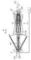
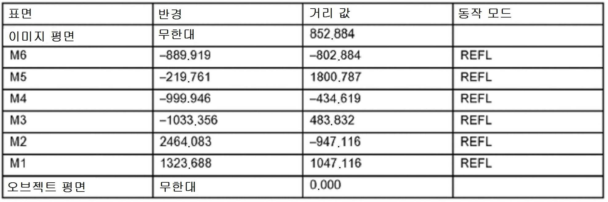
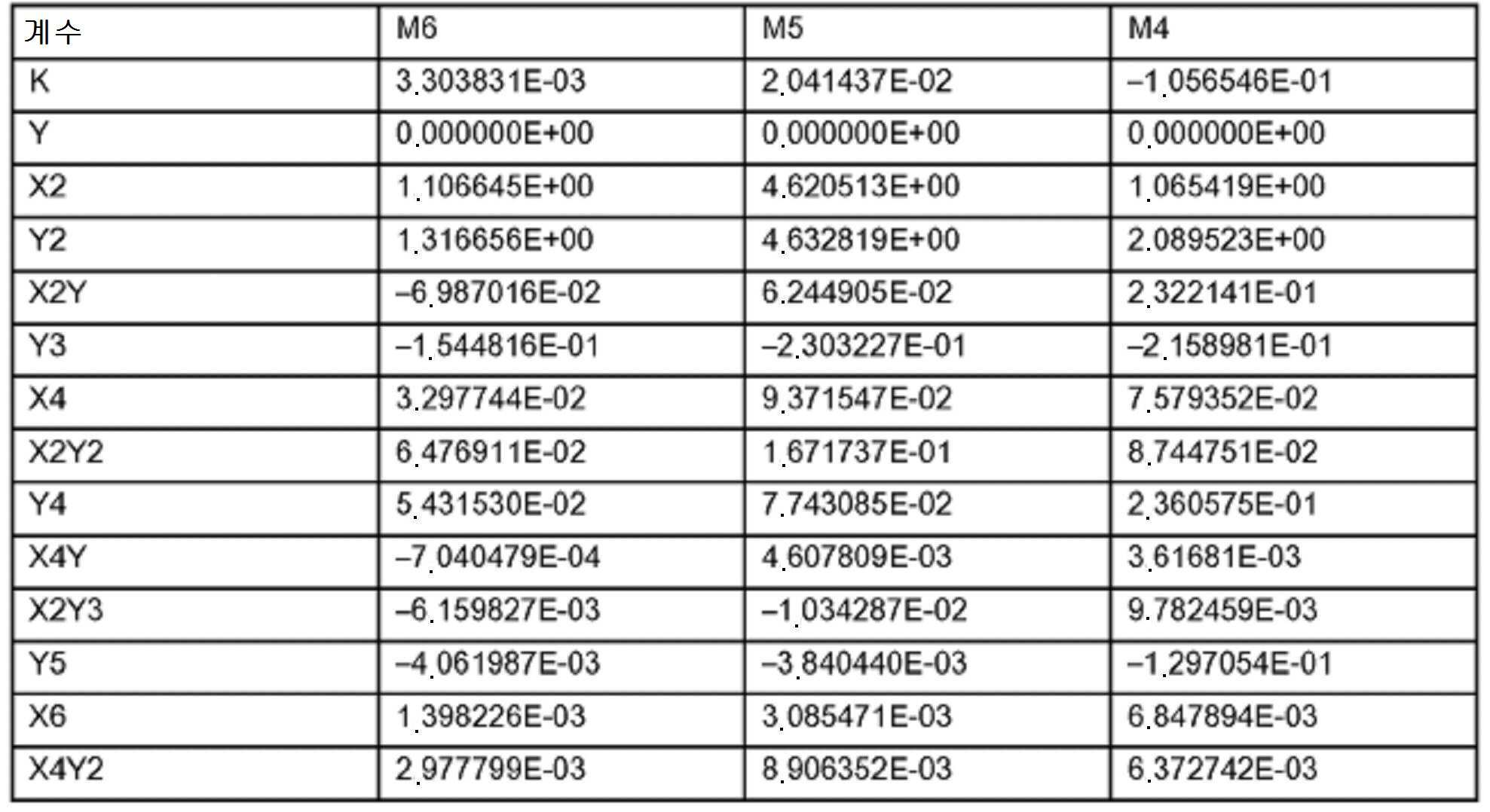
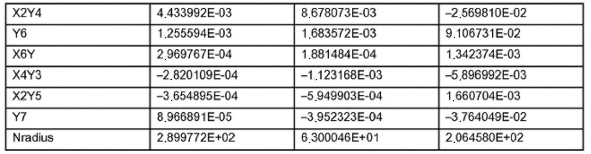
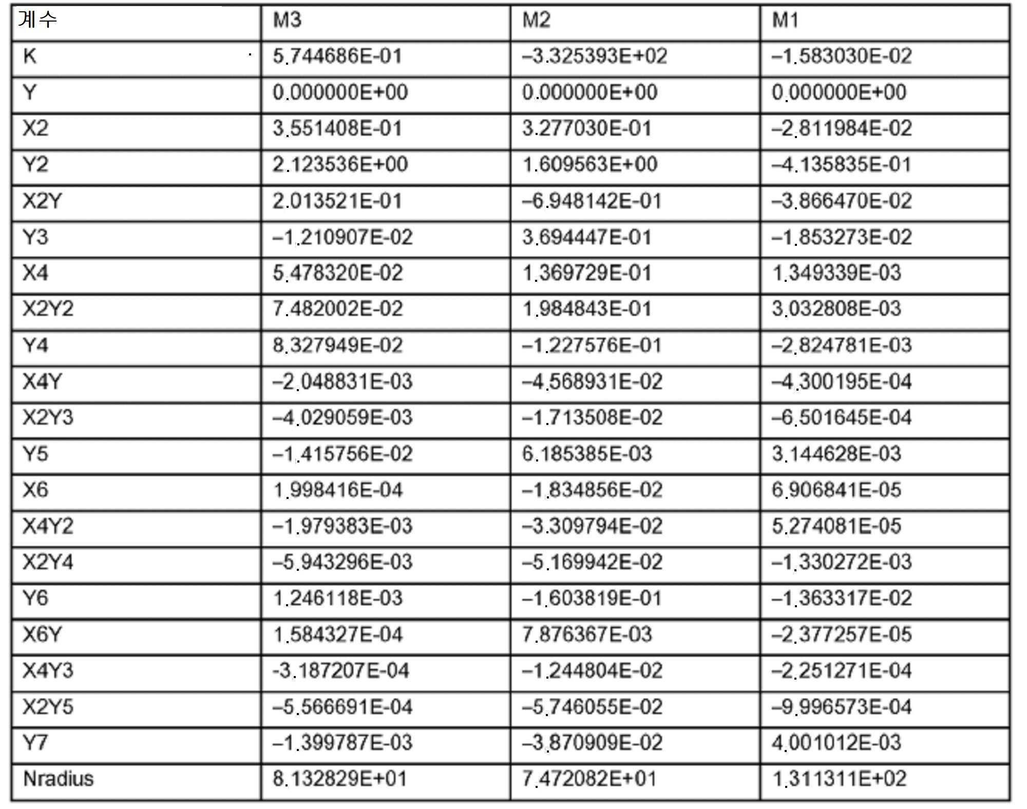
도 1은 EUV 마이크로리소그래피용 투영 노광 장치의 단면을 개략적으로 도시한다.
도 2는 일 예시적인 실시예에 따른 애너모픽 투영 렌즈의 빔 경로를 도시하기 위한 도 1에 따른 투영 노광 장치로부터의 발췌를 개략적으로 도시한다.
도 3은 그로부터 수직인 평면으로 도 2에 상응하는 도면을 도시한다.
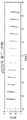
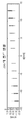
도 4는 도 4a 및 도 4b에서, 직사각형 필드를 갖는 이소모픽 투영 노광 장치의 형태로 기준 시스템(본 발명과 관련 없음)을 기초로 한 특정 효과를 설명하기 위한 이미지 수차 다이어그램을 도시하고, 도 4a는 z-축(제 1 회전축)에 대한 1μrad 만큼의 마스크의 회전의 경우의 이미지 수차(Z2 및 Z3)의 필드 변형을 도시하며, 도 4b는 제 2 회전축(z-축)에 대한 1μrad 만큼의 기판의 회전의 경우에 대한 상응하는 다이어그램을 도시한다.
도 5는 정확하게 곡면 링형 필드(arcuately curved ring field)를 갖는 이소모픽 렌즈(본 발명과 관련 없음)의 경우에 마스크 및 기판의 상응하는 회전을 도 5a 및 도 5b로 도시한다.
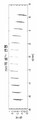
도 6은 링형 필드를 갖는 애너모픽 투영 렌즈의 예시적인 실시예의 경우에 대하여 도 5a 및 도 5b에서의 다이어그램과 상응하는 이미지 수차 다이어그램을 도 6a 및 도 6b로 도시하며, 여기서, 도 6a는 z-축에 대하여 1μrad 만큼의 마스크의 회전의 경우의 Z2 및 Z3의 결과적인 필드 변형을 도시하며, 도 6b는 1μrad 만큼의 기판의 회전의 경우의 Z2 및 Z3의 필드 변형의 상응하는 이미지 수차 다이어그램을 도시한다.
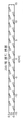
도 7은 z-축에 대하여 각각의 경우에 1μrad 만큼의 마스크 및 기판의 회전의 경우에 대한 Z2 및 Z3의 필드 변형의 이미지 수차 다이어그램을 도시한다.
도 8은 링형 필드를 갖는 애너모픽 투영 렌즈의 예시적인 실시예에서, 각각의 경우에 관련된 회전축(z-축)에 대하여 2μrad 만큼의 기판의 회전 및 1μrad 만큼의 마스크의 회전의 경우에 대한 이미지 수차를 도시한다.
도 9는 링형 필드를 갖는 애너모픽 투영 렌즈의 예시적인 실시예에서, 각각의 경우에 관련된 회전축(z-축)에 대하여 1μrad 만큼의 기판의 회전 및 2μrad 만큼의 마스크의 회전의 경우에 대한 이미지 수차 다이어그램을 도시한다.
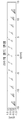
도 10은 직사각형 필드를 갖는 애너모픽 투영 렌즈의 예시적인 실시예에서, 각각의 경우에 관련된 회전축(z-축)에 대하여 2μrad 만큼의 기판의 회전 및 1μrad 만큼의 마스크의 회전의 경우에 대한 이미지 수차 다이어그램을 도시한다.
도 11은 직사각형 필드를 갖는 애너모픽 투영 렌즈의 예시적인 실시예에서, 각각의 경우에 관련된 회전축(z-축)에 대하여 1μrad만큼의 기판의 회전 및 2μrad 만큼의 마스크의 회전의 경우에 대한 이미지 수차 다이어그램을 도시한다.

Claims (5)
- 애너모픽(anamorphic) 투영 렌즈를 갖는 투영 노광 장치에서 마스크의 패턴의 적어도 하나의 이미지로 감방사선(radiation-sensitive) 기판을 노광하기 위한 투영 노광 방법으로서:
상기 패턴이 상기 투영 렌즈의 오브젝트 평면의 영역에 배열되도록 상기 투영 노광 장치의 조명 시스템과 상기 투영 렌즈 사이에 상기 마스크를 제공하는 단계;
상기 기판의 감방사선 표면이, 상기 오브젝트 평면과 광학적으로 켤레인 상기 투영 렌즈의 이미지 평면의 영역에 배열되도록 상기 기판을 홀드하는 단계;
상기 조명 시스템에 의해 제공되는 조명 방사선으로 상기 마스크의 조명 영역을 조명하는 단계;
상기 투영 렌즈에 의해 상기 기판에서의 이미지 필드 상에 상기 조명 영역에 놓인 상기 패턴의 일부를 투영하는 단계;
스캔 동작 동안 각각의 스캐닝 방향으로 상기 마스크와 상기 기판을 동기적으로 움직이는 단계;
상기 오브젝트 평면에 수직으로 배향되는 제 1 회전축에 대하여, 제 1 회전각만큼 상기 마스크를 회전시키는 단계;
상기 이미지 평면에 수직으로 배향되는 제 2 회전축에 대하여, 제 2 회전각만큼 조정된 방식으로 상기 기판을 회전시키는 단계를 포함하고,
상기 마스크의 회전에 의해 유발되는 적어도 하나의 제 1 이미지 수차에 대해, 상기 이미지 필드에 걸쳐 프로파일이 설정되고, 상기 마스크의 회전에 의해 유발되는 적어도 하나의 제 2 이미지 수차에 대해, 상기 이미지 필드에 걸친 프로파일이 상기 이미지 필드에 걸친 제 1 이미지 수차의 프로파일보다 더 큰 범위로 상기 기판의 회전에 의해 보상되도록, 상기 마스크와 상기 기판의 회전이 서로 조정되는, 투영 노광 방법. - 청구항 1에 있어서, 일 방향으로 진행하는 스캔 동작의 시작과 종료 사이의 시간 간격에서, 상기 기판의 회전 및 상기 마스크의 회전이 미리 규정가능한 움직임 프로파일에 따른 제 1 회전각과 제 2 회전각의 변동과 더불어 동기적으로 행해지는 방식으로, 상기 마스크 및 상기 기판은 스캔 동작 동안 할당된 회전축들에 대하여 동기적으로 회전하는, 투영 노광 방법.
- 청구항 1 또는 청구항 2에 있어서, 상기 투영 렌즈는 제 1 방향으로의 제 1 이미징 스케일 및 제 1 방향에 수직인 제 2 방향으로의, 상기 제 1 이미징 스케일로부터 벗어나는 제 2 이미징 스케일을 가지며, 상기 제 1 회전각과 상기 제 2 회전각은 서로, 상기 제 1 이미징 스케일과 상기 제 2 이미징 스케일의 비율에 또는 이러한 비율의 역(reciprocal)에 상응하는 비율인, 투영 노광 방법.
- 마스크(M)의 패턴의 적어도 하나의 이미지로 감방사선 기판(W)을 노광하기 위한 투영 노광 장치(WSC)로서,
주 방사선원(RS)의 주 방사선을 수광하고 상기 마스크(M) 상으로 보내지는 조명 방사선을 생성하기 위한 조명 시스템(ILL);
애너모픽 투영 렌즈(PO)로서, 상기 애너모픽 투영 렌즈의 이미지 평면(IS)의 영역에 상기 패턴의 이미지를 생성하기 위한 상기 애너모픽 투영 렌즈(PO);
상기 패턴이 상기 투영 렌즈의 오브젝트 평면(OS)의 영역에 배열되며 상기 투영 렌즈의 기준 축(AX)에 수직인 스캐닝 방향으로 움직일 수 있도록 상기 조명 시스템과 상기 투영 렌즈 사이에서 마스크를 홀드하기 위한 마스크 홀드 유닛(RST);
상기 기판의 감방사선 표면이 상기 투영 렌즈의 이미지 평면(IS) - 상기 이미지 평면(IS)은 상기 오브젝트 평면에 광학적으로 켤레임 - 의 영역에 배열되며 상기 투영 렌즈의 기준축에 수직으로 상기 마스크와 동기적으로 움직일 수 있도록, 상기 기판을 홀드하기 위한 기판 홀드 유닛(WST)을 포함하고,
상기 마스크 홀드 유닛(RST)은, 상기 오브젝트 평면(OS)에 관하여 직교로 나아가는 제 1 회전축(RA1)에 대한 상기 마스크의 제어된 회전을 위한 제 1 회전 유닛(ROT1)을 갖고,;
상기 기판 홀드 유닛(WST)은, 상기 이미지 평면(IS)에 관하여 직교로 나아가는 제 2 회전축(RA2)에 대한 상기 기판의 제어된 회전을 위한 제 2 회전 유닛(ROT2)을 가지며;
상기 마스크의 회전에 의해 유발되는 적어도 하나의 제 1 이미지 수차에 대해, 이미지 필드에 걸쳐 프로파일이 설정되고, 상기 마스크의 회전에 의해 유발되는 적어도 하나의 제 2 이미지 수차에 대해, 상기 이미지 필드에 걸친 프로파일이 상기 이미지 필드에 걸친 제 1 이미지 수차의 프로파일보다 더 큰 범위로 상기 기판의 회전에 의해 보상되도록, 상기 투영 노광 장치의 제어 유닛(CU)이 상기 마스크 홀드 유닛과 상기 기판 홀드 유닛을 서로 조정되는 방식으로 회전시키도록 구성되는, 투영 노광 장치. - 청구항 4에 있어서, 일 방향으로 진행하는 스캔 동작의 시작과 종료 사이의 시간 간격에서, 상기 기판의 회전과 상기 마스크의 회전을 미리 규정가능한 움직임 프로파일에 따라 제어가능하도록, 상기 제 1 회전 유닛(ROT1) 및 상기 제 2 회전 유닛(ROT2)은 동적으로(dynamically) 설계되는 것을 특징으로 하는, 투영 노광 장치.
Applications Claiming Priority (2)
| Application Number | Priority Date | Filing Date | Title |
|---|---|---|---|
| DE102016205617.4 | 2016-04-05 | ||
| DE102016205617.4A DE102016205617A1 (de) | 2016-04-05 | 2016-04-05 | Projektionsbelichtungsverfahren und Projektionsbelichtungsanlage |
Publications (2)
| Publication Number | Publication Date |
|---|---|
| KR20170114976A true KR20170114976A (ko) | 2017-10-16 |
| KR102408217B1 KR102408217B1 (ko) | 2022-06-13 |
Family
ID=59886063
Family Applications (1)
| Application Number | Title | Priority Date | Filing Date |
|---|---|---|---|
| KR1020170043741A Active KR102408217B1 (ko) | 2016-04-05 | 2017-04-04 | 투영 노광 방법 및 투영 노광 장치 |
Country Status (3)
| Country | Link |
|---|---|
| US (1) | US9933710B2 (ko) |
| KR (1) | KR102408217B1 (ko) |
| DE (1) | DE102016205617A1 (ko) |
Families Citing this family (4)
| Publication number | Priority date | Publication date | Assignee | Title |
|---|---|---|---|---|
| DE102018207277A1 (de) * | 2018-05-09 | 2019-11-14 | Carl Zeiss Smt Gmbh | Lithografiemaske, optisches System zur Übertragung von Original Strukturabschnitten der Lithografiemaske sowie Projektionsoptik zur Abbildung eines Objektfeldes, in dem mindestens ein Original-Strukturabschnitt einer Lithografiemaske anordenbar ist |
| DE102019205271A1 (de) * | 2019-04-11 | 2020-10-15 | Carl Zeiss Smt Gmbh | Abbildende Optik zur Abbildung eines Objektfeldes in ein Bildfeld sowie Projektionsbelichtungsanlage mit einer derartigen abbildenden Optik |
| US11644757B2 (en) * | 2019-12-19 | 2023-05-09 | Intel Corporation | Method to achieve tilted patterning with a through resist thickness using projection optics |
| US11579539B2 (en) * | 2021-03-03 | 2023-02-14 | Taiwan Semiconductor Manufacturing Company, Ltd. | Method and apparatus for improving critical dimension variation |
Citations (4)
| Publication number | Priority date | Publication date | Assignee | Title |
|---|---|---|---|---|
| JPH0774094A (ja) * | 1994-06-20 | 1995-03-17 | Nikon Corp | 投影露光装置及び方法 |
| KR19980033029A (ko) * | 1996-10-21 | 1998-07-25 | 요시다 쇼이치로 | 노광장치 및 노광방법 |
| JPH11154645A (ja) * | 1998-09-14 | 1999-06-08 | Nikon Corp | 走査露光装置及び方法 |
| WO2011120821A1 (en) * | 2010-03-30 | 2011-10-06 | Carl Zeiss Smt Gmbh | Method for operating a projection exposure apparatus with correction of imaging aberrations induced by the mask |
Family Cites Families (4)
| Publication number | Priority date | Publication date | Assignee | Title |
|---|---|---|---|---|
| WO1999026278A1 (en) | 1997-11-14 | 1999-05-27 | Nikon Corporation | Exposure apparatus and method of manufacturing the same, and exposure method |
| DE102004014766A1 (de) | 2003-04-02 | 2004-10-21 | Carl Zeiss Smt Ag | Verfahren zur Verzeichnungskorrektur in einer mikrolithographischen Projektionsbelichtungsanlage |
| TWI366004B (en) | 2005-09-13 | 2012-06-11 | Zeiss Carl Smt Gmbh | Microlithography projection optical system, microlithographic tool comprising such an optical system, method for microlithographic production of microstructured components using such a microlithographic tool, microstructured component being produced by s |
| DE102010040811A1 (de) | 2010-09-15 | 2012-03-15 | Carl Zeiss Smt Gmbh | Abbildende Optik |
-
2016
- 2016-04-05 DE DE102016205617.4A patent/DE102016205617A1/de not_active Withdrawn
-
2017
- 2017-03-27 US US15/470,007 patent/US9933710B2/en active Active
- 2017-04-04 KR KR1020170043741A patent/KR102408217B1/ko active Active
Patent Citations (4)
| Publication number | Priority date | Publication date | Assignee | Title |
|---|---|---|---|---|
| JPH0774094A (ja) * | 1994-06-20 | 1995-03-17 | Nikon Corp | 投影露光装置及び方法 |
| KR19980033029A (ko) * | 1996-10-21 | 1998-07-25 | 요시다 쇼이치로 | 노광장치 및 노광방법 |
| JPH11154645A (ja) * | 1998-09-14 | 1999-06-08 | Nikon Corp | 走査露光装置及び方法 |
| WO2011120821A1 (en) * | 2010-03-30 | 2011-10-06 | Carl Zeiss Smt Gmbh | Method for operating a projection exposure apparatus with correction of imaging aberrations induced by the mask |
Also Published As
| Publication number | Publication date |
|---|---|
| DE102016205617A1 (de) | 2017-10-05 |
| KR102408217B1 (ko) | 2022-06-13 |
| US20170285493A1 (en) | 2017-10-05 |
| US9933710B2 (en) | 2018-04-03 |
Similar Documents
| Publication | Publication Date | Title |
|---|---|---|
| JP7208953B2 (ja) | Euvマイクロリソグラフィのための投影レンズ、投影露光装置、及び投影露光方法 | |
| US10120176B2 (en) | Catadioptric projection objective comprising deflection mirrors and projection exposure method | |
| KR101515663B1 (ko) | 결상 광학 시스템 및 이러한 유형의 결상 광학 시스템을 갖는 마이크로리소그래피용 투영 노광 장치 | |
| CN102754009B (zh) | 成像光学部件 | |
| KR102408217B1 (ko) | 투영 노광 방법 및 투영 노광 장치 | |
| EP2000840A2 (en) | Projection optical system, exposure apparatus and device manufacturing method | |
| KR101892766B1 (ko) | 반사 결상 광학계, 노광 장치 및 디바이스 제조 방법 | |
| CN102171614B (zh) | 具有至少两个操作状态的微光刻投射曝光设备 | |
| CN119781253A (zh) | 用于操作微光刻投射曝光设备的方法、微光刻掩模和投射曝光设备 | |
| CN116368419A (zh) | 光学元件的支撑 | |
| WO2012137699A1 (ja) | 光学装置、露光装置、およびデバイス製造方法 |
Legal Events
| Date | Code | Title | Description |
|---|---|---|---|
| PA0109 | Patent application |
Patent event code: PA01091R01D Comment text: Patent Application Patent event date: 20170404 |
|
| PG1501 | Laying open of application | ||
| A201 | Request for examination | ||
| PA0201 | Request for examination |
Patent event code: PA02012R01D Patent event date: 20200403 Comment text: Request for Examination of Application Patent event code: PA02011R01I Patent event date: 20170404 Comment text: Patent Application |
|
| E902 | Notification of reason for refusal | ||
| PE0902 | Notice of grounds for rejection |
Comment text: Notification of reason for refusal Patent event date: 20210909 Patent event code: PE09021S01D |
|
| E701 | Decision to grant or registration of patent right | ||
| PE0701 | Decision of registration |
Patent event code: PE07011S01D Comment text: Decision to Grant Registration Patent event date: 20220322 |
|
| GRNT | Written decision to grant | ||
| PR0701 | Registration of establishment |
Comment text: Registration of Establishment Patent event date: 20220608 Patent event code: PR07011E01D |
|
| PR1002 | Payment of registration fee |
Payment date: 20220609 End annual number: 3 Start annual number: 1 |
|
| PG1601 | Publication of registration |