KR20170116211A - 발광소자 - Google Patents
발광소자 Download PDFInfo
- Publication number
- KR20170116211A KR20170116211A KR1020177027521A KR20177027521A KR20170116211A KR 20170116211 A KR20170116211 A KR 20170116211A KR 1020177027521 A KR1020177027521 A KR 1020177027521A KR 20177027521 A KR20177027521 A KR 20177027521A KR 20170116211 A KR20170116211 A KR 20170116211A
- Authority
- KR
- South Korea
- Prior art keywords
- light emitting
- emitting diode
- array chip
- diode array
- submount
- Prior art date
- Legal status (The legal status is an assumption and is not a legal conclusion. Google has not performed a legal analysis and makes no representation as to the accuracy of the status listed.)
- Granted
Links
Images





Classifications
-
- H01L25/0753—
-
- H01L27/15—
-
- H01L33/52—
-
- H01L33/58—
-
- H01L33/62—
-
- H—ELECTRICITY
- H10—SEMICONDUCTOR DEVICES; ELECTRIC SOLID-STATE DEVICES NOT OTHERWISE PROVIDED FOR
- H10H—INORGANIC LIGHT-EMITTING SEMICONDUCTOR DEVICES HAVING POTENTIAL BARRIERS
- H10H20/00—Individual inorganic light-emitting semiconductor devices having potential barriers, e.g. light-emitting diodes [LED]
- H10H20/80—Constructional details
- H10H20/85—Packages
- H10H20/851—Wavelength conversion means
-
- H—ELECTRICITY
- H10—SEMICONDUCTOR DEVICES; ELECTRIC SOLID-STATE DEVICES NOT OTHERWISE PROVIDED FOR
- H10H—INORGANIC LIGHT-EMITTING SEMICONDUCTOR DEVICES HAVING POTENTIAL BARRIERS
- H10H20/00—Individual inorganic light-emitting semiconductor devices having potential barriers, e.g. light-emitting diodes [LED]
- H10H20/80—Constructional details
- H10H20/85—Packages
- H10H20/852—Encapsulations
-
- H—ELECTRICITY
- H10—SEMICONDUCTOR DEVICES; ELECTRIC SOLID-STATE DEVICES NOT OTHERWISE PROVIDED FOR
- H10H—INORGANIC LIGHT-EMITTING SEMICONDUCTOR DEVICES HAVING POTENTIAL BARRIERS
- H10H20/00—Individual inorganic light-emitting semiconductor devices having potential barriers, e.g. light-emitting diodes [LED]
- H10H20/80—Constructional details
- H10H20/85—Packages
- H10H20/855—Optical field-shaping means, e.g. lenses
-
- H—ELECTRICITY
- H10—SEMICONDUCTOR DEVICES; ELECTRIC SOLID-STATE DEVICES NOT OTHERWISE PROVIDED FOR
- H10H—INORGANIC LIGHT-EMITTING SEMICONDUCTOR DEVICES HAVING POTENTIAL BARRIERS
- H10H20/00—Individual inorganic light-emitting semiconductor devices having potential barriers, e.g. light-emitting diodes [LED]
- H10H20/80—Constructional details
- H10H20/85—Packages
- H10H20/857—Interconnections, e.g. lead-frames, bond wires or solder balls
-
- H—ELECTRICITY
- H10—SEMICONDUCTOR DEVICES; ELECTRIC SOLID-STATE DEVICES NOT OTHERWISE PROVIDED FOR
- H10H—INORGANIC LIGHT-EMITTING SEMICONDUCTOR DEVICES HAVING POTENTIAL BARRIERS
- H10H29/00—Integrated devices, or assemblies of multiple devices, comprising at least one light-emitting semiconductor element covered by group H10H20/00
- H10H29/10—Integrated devices comprising at least one light-emitting semiconductor component covered by group H10H20/00
-
- H—ELECTRICITY
- H10—SEMICONDUCTOR DEVICES; ELECTRIC SOLID-STATE DEVICES NOT OTHERWISE PROVIDED FOR
- H10H—INORGANIC LIGHT-EMITTING SEMICONDUCTOR DEVICES HAVING POTENTIAL BARRIERS
- H10H29/00—Integrated devices, or assemblies of multiple devices, comprising at least one light-emitting semiconductor element covered by group H10H20/00
- H10H29/10—Integrated devices comprising at least one light-emitting semiconductor component covered by group H10H20/00
- H10H29/14—Integrated devices comprising at least one light-emitting semiconductor component covered by group H10H20/00 comprising multiple light-emitting semiconductor components
-
- H—ELECTRICITY
- H10—SEMICONDUCTOR DEVICES; ELECTRIC SOLID-STATE DEVICES NOT OTHERWISE PROVIDED FOR
- H10K—ORGANIC ELECTRIC SOLID-STATE DEVICES
- H10K59/00—Integrated devices, or assemblies of multiple devices, comprising at least one organic light-emitting element covered by group H10K50/00
- H10K59/30—Devices specially adapted for multicolour light emission
- H10K59/35—Devices specially adapted for multicolour light emission comprising red-green-blue [RGB] subpixels
-
- H—ELECTRICITY
- H10—SEMICONDUCTOR DEVICES; ELECTRIC SOLID-STATE DEVICES NOT OTHERWISE PROVIDED FOR
- H10W—GENERIC PACKAGES, INTERCONNECTIONS, CONNECTORS OR OTHER CONSTRUCTIONAL DETAILS OF DEVICES COVERED BY CLASS H10
- H10W90/00—Package configurations
-
- H01L2224/48091—
-
- H01L2224/48137—
-
- H01L2224/8592—
-
- H01L2924/12032—
-
- H01L2924/30107—
-
- H—ELECTRICITY
- H10—SEMICONDUCTOR DEVICES; ELECTRIC SOLID-STATE DEVICES NOT OTHERWISE PROVIDED FOR
- H10H—INORGANIC LIGHT-EMITTING SEMICONDUCTOR DEVICES HAVING POTENTIAL BARRIERS
- H10H29/00—Integrated devices, or assemblies of multiple devices, comprising at least one light-emitting semiconductor element covered by group H10H20/00
- H10H29/10—Integrated devices comprising at least one light-emitting semiconductor component covered by group H10H20/00
- H10H29/14—Integrated devices comprising at least one light-emitting semiconductor component covered by group H10H20/00 comprising multiple light-emitting semiconductor components
- H10H29/142—Two-dimensional arrangements, e.g. asymmetric LED layout
-
- H—ELECTRICITY
- H10—SEMICONDUCTOR DEVICES; ELECTRIC SOLID-STATE DEVICES NOT OTHERWISE PROVIDED FOR
- H10W—GENERIC PACKAGES, INTERCONNECTIONS, CONNECTORS OR OTHER CONSTRUCTIONAL DETAILS OF DEVICES COVERED BY CLASS H10
- H10W72/00—Interconnections or connectors in packages
- H10W72/01—Manufacture or treatment
- H10W72/015—Manufacture or treatment of bond wires
- H10W72/01515—Forming coatings
-
- H—ELECTRICITY
- H10—SEMICONDUCTOR DEVICES; ELECTRIC SOLID-STATE DEVICES NOT OTHERWISE PROVIDED FOR
- H10W—GENERIC PACKAGES, INTERCONNECTIONS, CONNECTORS OR OTHER CONSTRUCTIONAL DETAILS OF DEVICES COVERED BY CLASS H10
- H10W72/00—Interconnections or connectors in packages
- H10W72/071—Connecting or disconnecting
- H10W72/075—Connecting or disconnecting of bond wires
-
- H—ELECTRICITY
- H10—SEMICONDUCTOR DEVICES; ELECTRIC SOLID-STATE DEVICES NOT OTHERWISE PROVIDED FOR
- H10W—GENERIC PACKAGES, INTERCONNECTIONS, CONNECTORS OR OTHER CONSTRUCTIONAL DETAILS OF DEVICES COVERED BY CLASS H10
- H10W90/00—Package configurations
- H10W90/701—Package configurations characterised by the relative positions of pads or connectors relative to package parts
- H10W90/751—Package configurations characterised by the relative positions of pads or connectors relative to package parts of bond wires
- H10W90/753—Package configurations characterised by the relative positions of pads or connectors relative to package parts of bond wires between laterally-adjacent chips
Landscapes
- Led Devices (AREA)
- Led Device Packages (AREA)
- Circuit Arrangement For Electric Light Sources In General (AREA)
Abstract
Description
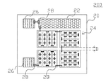
도 2a는 본 발명의 실시예의 평면 구조를 나타낸 개략도이다
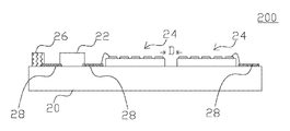
도 2b는 본 발명의 실시예의 측면 구조를 나타낸 개략도이다.
도 2c는 본 발명의 다른 실시예의 측면 구조를 나타낸 개략도이다.
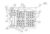
도 3은 본 발명의 또 다른 실시예의 평면 구조를 나타낸 개략도이다
도 4는 본 발명의 발광다이오드 어레이 칩의 측면 구조를 나타낸 개략도이다.
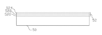
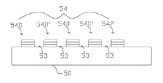
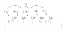
도 5a ~ 도 5d는 본 발명의 실시예의 발광다이오드 어레이 칩의 제조 공정을 나타낸 개략도이다.
도 6은 본 발명의 실시예의 발광다이오드 어레이 칩의 평면 구조를 나타낸 개략도이다.
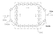
도 7a와 도 7b는 본 발명의 실시예의 발광다이오드 어레이 칩의 전기 회로를 나타낸 개략도이다.
도 8은 본 발명의 실시예의 발광다이오드 어레이 칩의 다른 전기 회로를 나타낸 개략도이다.
| 실시예 번호 |
교류 전력 시스템 | 파랑 발광다이오드 어레이 칩 수량 | 파랑 발광다이오드 유닛 수량 | 빨강 발광다이오드 어레이 칩 수량 | 빨강 발광다이오드 유닛 수량 |
| 1 | AC110V | 2 | 12 | 2 | 6 |
| 2 | AC110V | 3 | 8 | 1 | 12 |
| 3 | AC220V | 2 | 24 | 2 | 12 |
| 4 | AC220V | 3 | 16 | 1 | 24 |
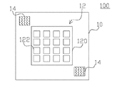
12 : 발광다이오드 어레이 칩
120 : 기판
200 : 발광소자
21 : 반사층
23 : 파장 변환층
25 : 밀봉재
28 : 도전성 회선
30 : 서브 마운트
32 : 발광다이오드 어레이 칩
36 : 커패시터
39 : 도전성 회선
40 : 기판
44 : 전극
500 : 발광다이오드 어레이 칩
52 : 에피텍셜 적층
522 : 활성층
54 : 다이오드 유닛
540 : 발광다이오드 유닛
56 : 전극
580 : 절연층
542a : 정류다이오드 유닛
542c : 정류다이오드 유닛
56a : 전극
10 : 서브 마운트
14 : 본딩 패드
122 : 발광다이오드 유닛
20 : 서브 마운트
22 : 전자소자
24 : 발광다이오드 어레이 칩
26 : 본딩 패드
300 : 발광소자
31 : 정류소자
34 : 레지스터
38 : 본딩 패드
400 : 발광다이오드 어레이 칩
42 : 발광다이오드 어레이 칩
46 : 전기 접속 구조
50 : 기판
520 : 제1 도전형 반도체층
524 : 제2 도전형 반도체층
540 : 발광다이오드 유닛
542 : 정류다이오드 유닛
58 : 전기 접속 구조
582 : 금속층
542b : 정류다이오드 유닛
542d : 정류다이오드 유닛
56b : 전극
Claims (10)
- 마운트;
복수 개의 발광다이오드 유닛을 포함하고, 상기 마운트 상에 위치하는 제1 발광다이오드 어레이 칩;
상기 마운트 상에 위치하고, 상기 제1 발광다이오드 어레이 칩 사이의 거리가 10um보다 큰 제2 발광다이오드 어레이 칩;
상기 마운트 상에 위치하고, 상기 제1 발광다이오드 어레이 칩 및 상기 제2 발광다이오드 어레이 칩과 전기적 연결을 형성하는 도전성 회선;
상기 마운트 상에 위치하고, 상기 도전성 회선과 전기적 연결을 형성하는 본딩 패드; 및
상기 제1 발광다이오드 어레이 칩 및 상기 제2 발광다이오드 어레이 칩을 연속적으로 피복하는 패키징 고무 재료
를 포함하는 발광소자. - 제1항에 있어서,
상기 복수 개의 발광다이오드 유닛은 동일한 에피텍셜 적층을 구비하는, 발광소자. - 제1항에 있어서,
상기 마운트는 상기 제1 발광다이오드 어레이 칩과 상기 제2 발광다이오드 어레이 칩을 수용하는 함몰 구조를 구비하는, 발광소자. - 제1항에 있어서,
상기 제1 발광다이오드 어레이 칩 상에 설치되는 제1 파장 변환층을 더 포함하는 발광소자. - 제4항에 있어서,
상기 제2 발광다이오드 어레이 칩 상에 설치되고, 상기 제1 파장 변환층과 물리적으로 분리되는 제2 파장 변환층을 더 포함하는 발광소자. - 제1항에 있어서,
상기 복수 개의 발광다이오드 유닛은 공통의 성장 기판을 구비하는, 발광소자. - 제1항에 있어서,
상기 패키징 고무 재료는 상기 본딩 패드를 노출시키는, 발광소자. - 제1항에 있어서,
상기 제2 발광다이오드 어레이 칩과 상기 제1 발광다이오드 어레이 칩은 서로 상이한 피크 값 파장을 가지는, 발광소자. - 제5항에 있어서,
상기 마운트 상에 위치하는 전자소자를 더 포함하고, 상기 전자소자는 저항, 커패시턴스, 또는 인덕턴스를 포함하는, 발광소자. - 제1항에 있어서,
상기 마운트와 상기 제1 발광다이오드 어레이 칩 사이에 형성되는 반사층을 더 포함하는 발광소자.
Applications Claiming Priority (3)
| Application Number | Priority Date | Filing Date | Title |
|---|---|---|---|
| TW200910007059.2 | 2009-02-09 | ||
| CN200910007059.2A CN101800219B (zh) | 2009-02-09 | 2009-02-09 | 发光元件 |
| PCT/CN2009/074422 WO2010088823A1 (zh) | 2009-02-09 | 2009-10-13 | 发光元件 |
Related Parent Applications (1)
| Application Number | Title | Priority Date | Filing Date |
|---|---|---|---|
| KR1020167021072A Division KR101784901B1 (ko) | 2009-02-09 | 2009-10-13 | 발광 소자 |
Publications (2)
| Publication Number | Publication Date |
|---|---|
| KR20170116211A true KR20170116211A (ko) | 2017-10-18 |
| KR102116359B1 KR102116359B1 (ko) | 2020-05-29 |
Family
ID=42541660
Family Applications (3)
| Application Number | Title | Priority Date | Filing Date |
|---|---|---|---|
| KR1020177027521A Active KR102116359B1 (ko) | 2009-02-09 | 2009-10-13 | 발광소자 |
| KR1020167021072A Active KR101784901B1 (ko) | 2009-02-09 | 2009-10-13 | 발광 소자 |
| KR1020117020892A Active KR101646633B1 (ko) | 2009-02-09 | 2009-10-13 | 발광 소자 |
Family Applications After (2)
| Application Number | Title | Priority Date | Filing Date |
|---|---|---|---|
| KR1020167021072A Active KR101784901B1 (ko) | 2009-02-09 | 2009-10-13 | 발광 소자 |
| KR1020117020892A Active KR101646633B1 (ko) | 2009-02-09 | 2009-10-13 | 발광 소자 |
Country Status (5)
| Country | Link |
|---|---|
| US (2) | US9142534B2 (ko) |
| KR (3) | KR102116359B1 (ko) |
| CN (3) | CN101800219B (ko) |
| DE (1) | DE112009004359B4 (ko) |
| WO (1) | WO2010088823A1 (ko) |
Families Citing this family (18)
| Publication number | Priority date | Publication date | Assignee | Title |
|---|---|---|---|---|
| CN101800219B (zh) | 2009-02-09 | 2019-09-17 | 晶元光电股份有限公司 | 发光元件 |
| CN101958316B (zh) * | 2010-07-20 | 2013-01-16 | 上海亚明灯泡厂有限公司 | Led集成封装光源模块 |
| US20120269520A1 (en) | 2011-04-19 | 2012-10-25 | Hong Steve M | Lighting apparatuses and led modules for both illumation and optical communication |
| TWI478358B (zh) * | 2011-08-04 | 2015-03-21 | Univ Nat Central | A method of integrated AC - type light - emitting diode module |
| US10043960B2 (en) * | 2011-11-15 | 2018-08-07 | Cree, Inc. | Light emitting diode (LED) packages and related methods |
| CN103165589A (zh) * | 2011-12-08 | 2013-06-19 | 东莞柏泽光电科技有限公司 | 混光式多晶封装结构 |
| GB201202222D0 (en) * | 2012-02-09 | 2012-03-28 | Mled Ltd | Enhanced light extraction |
| CN103367384B (zh) * | 2012-03-30 | 2018-04-03 | 晶元光电股份有限公司 | 发光二极管元件 |
| CN103839511B (zh) * | 2012-11-21 | 2018-05-11 | 晶元光电股份有限公司 | 关于发光二极管的发光装置与驱动方法 |
| CN110335932A (zh) * | 2013-07-01 | 2019-10-15 | 晶元光电股份有限公司 | 发光二极管组件及制作方法 |
| TWI532215B (zh) * | 2013-12-26 | 2016-05-01 | 隆達電子股份有限公司 | 發光二極體元件 |
| TW201631808A (zh) * | 2015-02-25 | 2016-09-01 | 隆達電子股份有限公司 | 發光二極體晶片封裝體 |
| EP3273850B1 (en) * | 2015-03-23 | 2021-11-24 | Koninklijke Philips N.V. | Optical vital signs sensor |
| USD762596S1 (en) * | 2015-04-02 | 2016-08-02 | Genesis Photonics Inc. | Light emitting diode package substrate |
| TWI663724B (zh) * | 2017-01-26 | 2019-06-21 | Acer Incorporated | 發光二極體顯示器及其製造方法 |
| CN110164857B (zh) * | 2018-02-14 | 2024-04-09 | 晶元光电股份有限公司 | 发光装置 |
| DE102019219016A1 (de) | 2019-12-05 | 2021-06-10 | OSRAM Opto Semiconductors Gesellschaft mit beschränkter Haftung | Optoelektronische vorrichtung und verfahren zur herstellung einer optoelektronischen vorrichtung |
| CN111326632B (zh) * | 2020-03-08 | 2021-04-30 | 河北工业大学 | 具有梯形侧壁场板肖特基二极管的AC Micro-LED阵列 |
Citations (5)
| Publication number | Priority date | Publication date | Assignee | Title |
|---|---|---|---|---|
| KR20060098229A (ko) * | 2005-03-11 | 2006-09-18 | 서울반도체 주식회사 | 발광 장치 및 이의 제조 방법 |
| KR20070006073A (ko) * | 2005-07-07 | 2007-01-11 | 서울반도체 주식회사 | 발광 장치 |
| KR20070084464A (ko) * | 2004-11-25 | 2007-08-24 | 마츠시타 덴끼 산교 가부시키가이샤 | 반도체 발광장치, 조명장치, 휴대통신기기, 카메라 및제조방법 |
| JP2007537590A (ja) * | 2004-05-13 | 2007-12-20 | ソウル オプト デバイス カンパニー リミテッド | Rgb発光ダイオードと蛍光体を組み合わせた発光装置 |
| JP2008251663A (ja) * | 2007-03-29 | 2008-10-16 | Sharp Corp | 発光装置および照明装置 |
Family Cites Families (25)
| Publication number | Priority date | Publication date | Assignee | Title |
|---|---|---|---|---|
| GB1550012A (en) * | 1977-04-20 | 1979-08-08 | Gillette Co | Battery chargers |
| JPH0822081A (ja) * | 1994-07-08 | 1996-01-23 | Fuji Photo Film Co Ltd | 写真プリンタ及びフイルムスキャナー |
| WO2005022654A2 (en) | 2003-08-28 | 2005-03-10 | Matsushita Electric Industrial Co.,Ltd. | Semiconductor light emitting device, light emitting module, lighting apparatus, display element and manufacturing method of semiconductor light emitting device |
| CN2657203Y (zh) * | 2003-09-01 | 2004-11-17 | 光鼎电子股份有限公司 | 具整流电路的发光二极管封装装置 |
| US7064353B2 (en) * | 2004-05-26 | 2006-06-20 | Philips Lumileds Lighting Company, Llc | LED chip with integrated fast switching diode for ESD protection |
| US7462502B2 (en) * | 2004-11-12 | 2008-12-09 | Philips Lumileds Lighting Company, Llc | Color control by alteration of wavelength converting element |
| US7419839B2 (en) * | 2004-11-12 | 2008-09-02 | Philips Lumileds Lighting Company, Llc | Bonding an optical element to a light emitting device |
| JP4337731B2 (ja) * | 2004-12-22 | 2009-09-30 | ソニー株式会社 | 照明装置、及び画像表示装置 |
| US7221044B2 (en) * | 2005-01-21 | 2007-05-22 | Ac Led Lighting, L.L.C. | Heterogeneous integrated high voltage DC/AC light emitter |
| EP2280430B1 (en) * | 2005-03-11 | 2020-01-01 | Seoul Semiconductor Co., Ltd. | LED package having an array of light emitting cells coupled in series |
| KR101121727B1 (ko) | 2005-03-29 | 2012-06-05 | 서울반도체 주식회사 | 직렬접속된 발광셀 어레이를 갖는 발광다이오드 칩을탑재한 발광다이오드 패키지 |
| TW200723559A (en) * | 2005-12-13 | 2007-06-16 | Ind Tech Res Inst | Alternating current (AC) light emitting assembly and AC light emitting device |
| EP2750194A1 (en) * | 2005-06-22 | 2014-07-02 | Seoul Viosys Co., Ltd. | Light emitting device comprising a plurality of light emitting diode cells |
| KR100634307B1 (ko) * | 2005-08-10 | 2006-10-16 | 서울옵토디바이스주식회사 | 발광 소자 및 이의 제조 방법 |
| JP4462249B2 (ja) * | 2005-09-22 | 2010-05-12 | ソニー株式会社 | 発光ダイオードの製造方法、集積型発光ダイオードの製造方法および窒化物系iii−v族化合物半導体の成長方法 |
| JP4945112B2 (ja) * | 2005-10-28 | 2012-06-06 | スタンレー電気株式会社 | Led照明装置 |
| CN100565873C (zh) * | 2005-12-15 | 2009-12-02 | 鼎元光电科技股份有限公司 | 结合整流电路于次载具的发光二极管发光装置与制造方法 |
| US7359416B2 (en) * | 2006-03-15 | 2008-04-15 | Matsushita Electric Industrial Co., Ltd. | Optical semiconductor device |
| KR100854328B1 (ko) * | 2006-07-07 | 2008-08-28 | 엘지전자 주식회사 | 발광 소자 패키지 및 그 제조방법 |
| WO2008138015A2 (en) * | 2007-05-08 | 2008-11-13 | Occam Portfolio Llc | Light-emitting diode assembly without solder |
| KR100843402B1 (ko) | 2007-06-22 | 2008-07-03 | 삼성전기주식회사 | Led 구동회로 및 led 어레이 장치 |
| US8461613B2 (en) * | 2008-05-27 | 2013-06-11 | Interlight Optotech Corporation | Light emitting device |
| KR101025972B1 (ko) * | 2008-06-30 | 2011-03-30 | 삼성엘이디 주식회사 | 교류 구동 발광 장치 |
| US8035307B2 (en) * | 2008-11-03 | 2011-10-11 | Gt Biomescilt Light Limited | AC to DC LED illumination devices, systems and methods |
| CN101800219B (zh) | 2009-02-09 | 2019-09-17 | 晶元光电股份有限公司 | 发光元件 |
-
2009
- 2009-02-09 CN CN200910007059.2A patent/CN101800219B/zh active Active
- 2009-10-13 CN CN201510168949.7A patent/CN104900637B/zh active Active
- 2009-10-13 CN CN200980145677.1A patent/CN102257619B/zh active Active
- 2009-10-13 KR KR1020177027521A patent/KR102116359B1/ko active Active
- 2009-10-13 KR KR1020167021072A patent/KR101784901B1/ko active Active
- 2009-10-13 KR KR1020117020892A patent/KR101646633B1/ko active Active
- 2009-10-13 DE DE112009004359.3T patent/DE112009004359B4/de active Active
- 2009-10-13 WO PCT/CN2009/074422 patent/WO2010088823A1/zh not_active Ceased
- 2009-10-13 US US13/148,544 patent/US9142534B2/en active Active
-
2015
- 2015-08-18 US US14/829,262 patent/US10038029B2/en active Active
Patent Citations (5)
| Publication number | Priority date | Publication date | Assignee | Title |
|---|---|---|---|---|
| JP2007537590A (ja) * | 2004-05-13 | 2007-12-20 | ソウル オプト デバイス カンパニー リミテッド | Rgb発光ダイオードと蛍光体を組み合わせた発光装置 |
| KR20070084464A (ko) * | 2004-11-25 | 2007-08-24 | 마츠시타 덴끼 산교 가부시키가이샤 | 반도체 발광장치, 조명장치, 휴대통신기기, 카메라 및제조방법 |
| KR20060098229A (ko) * | 2005-03-11 | 2006-09-18 | 서울반도체 주식회사 | 발광 장치 및 이의 제조 방법 |
| KR20070006073A (ko) * | 2005-07-07 | 2007-01-11 | 서울반도체 주식회사 | 발광 장치 |
| JP2008251663A (ja) * | 2007-03-29 | 2008-10-16 | Sharp Corp | 発光装置および照明装置 |
Also Published As
| Publication number | Publication date |
|---|---|
| US20120049213A1 (en) | 2012-03-01 |
| CN104900637A (zh) | 2015-09-09 |
| WO2010088823A1 (zh) | 2010-08-12 |
| US10038029B2 (en) | 2018-07-31 |
| US9142534B2 (en) | 2015-09-22 |
| KR101646633B1 (ko) | 2016-08-08 |
| KR20110121627A (ko) | 2011-11-07 |
| DE112009004359T5 (de) | 2012-05-24 |
| KR101784901B1 (ko) | 2017-10-12 |
| KR102116359B1 (ko) | 2020-05-29 |
| CN101800219B (zh) | 2019-09-17 |
| CN102257619B (zh) | 2015-05-13 |
| CN104900637B (zh) | 2018-07-13 |
| KR20160095205A (ko) | 2016-08-10 |
| CN102257619A (zh) | 2011-11-23 |
| DE112009004359B4 (de) | 2021-05-06 |
| CN101800219A (zh) | 2010-08-11 |
| US20150357371A1 (en) | 2015-12-10 |
Similar Documents
| Publication | Publication Date | Title |
|---|---|---|
| KR101646633B1 (ko) | 발광 소자 | |
| CN101859758B (zh) | 高电压低电流面发射led | |
| US9076940B2 (en) | Solid state lighting component | |
| US9793247B2 (en) | Solid state lighting component | |
| US7148515B1 (en) | Light emitting device having integrated rectifier circuit in substrate | |
| US8283684B2 (en) | LED semiconductor body and use of an LED semiconductor body | |
| CN103038899A (zh) | 高电压低电流表面发射led | |
| TWI445156B (zh) | 發光元件 | |
| CN103782400A (zh) | 包括多组发光二极管的单片多结发光装置 | |
| TWI581398B (zh) | 發光元件 | |
| KR101537798B1 (ko) | 백색 발광 다이오드 패키지 | |
| CN101197389A (zh) | 交流发光体以及交流发光装置 | |
| CN100565873C (zh) | 结合整流电路于次载具的发光二极管发光装置与制造方法 | |
| CN100413071C (zh) | 使用交流电源的发光二极管灯及其制造方法 | |
| CN101211957A (zh) | 交流电发光装置及其制法 |
Legal Events
| Date | Code | Title | Description |
|---|---|---|---|
| A107 | Divisional application of patent | ||
| A201 | Request for examination | ||
| PA0104 | Divisional application for international application |
St.27 status event code: A-0-1-A10-A18-div-PA0104 St.27 status event code: A-0-1-A10-A16-div-PA0104 |
|
| PA0201 | Request for examination |
St.27 status event code: A-1-2-D10-D11-exm-PA0201 |
|
| PG1501 | Laying open of application |
St.27 status event code: A-1-1-Q10-Q12-nap-PG1501 |
|
| E902 | Notification of reason for refusal | ||
| PE0902 | Notice of grounds for rejection |
St.27 status event code: A-1-2-D10-D21-exm-PE0902 |
|
| AMND | Amendment | ||
| P11-X000 | Amendment of application requested |
St.27 status event code: A-2-2-P10-P11-nap-X000 |
|
| P13-X000 | Application amended |
St.27 status event code: A-2-2-P10-P13-nap-X000 |
|
| E601 | Decision to refuse application | ||
| PE0601 | Decision on rejection of patent |
St.27 status event code: N-2-6-B10-B15-exm-PE0601 |
|
| X091 | Application refused [patent] | ||
| AMND | Amendment | ||
| E13-X000 | Pre-grant limitation requested |
St.27 status event code: A-2-3-E10-E13-lim-X000 |
|
| P11-X000 | Amendment of application requested |
St.27 status event code: A-2-2-P10-P11-nap-X000 |
|
| P13-X000 | Application amended |
St.27 status event code: A-2-2-P10-P13-nap-X000 |
|
| PX0901 | Re-examination |
St.27 status event code: A-2-3-E10-E12-rex-PX0901 |
|
| E601 | Decision to refuse application | ||
| E801 | Decision on dismissal of amendment | ||
| PX0601 | Decision of rejection after re-examination |
St.27 status event code: N-2-6-B10-B17-rex-PX0601 |
|
| X601 | Decision of rejection after re-examination | ||
| R18-X000 | Changes to party contact information recorded |
St.27 status event code: A-3-3-R10-R18-oth-X000 |
|
| J201 | Request for trial against refusal decision | ||
| PJ0201 | Trial against decision of rejection |
St.27 status event code: A-3-3-V10-V11-apl-PJ0201 |
|
| J301 | Trial decision |
Free format text: TRIAL NUMBER: 2018101004036; TRIAL DECISION FOR APPEAL AGAINST DECISION TO DECLINE REFUSAL REQUESTED 20180928 Effective date: 20191001 |
|
| PJ1301 | Trial decision |
St.27 status event code: A-3-3-V10-V15-crt-PJ1301 Decision date: 20191001 Appeal event data comment text: Appeal Kind Category : Appeal against decision to decline refusal, Appeal Ground Text : 2017 7027521 Appeal request date: 20180928 Appellate body name: Patent Examination Board Decision authority category: Office appeal board Decision identifier: 2018101004036 |
|
| PS0901 | Examination by remand of revocation |
St.27 status event code: A-6-3-E10-E12-rex-PS0901 |
|
| S901 | Examination by remand of revocation | ||
| E902 | Notification of reason for refusal | ||
| PE0902 | Notice of grounds for rejection |
St.27 status event code: A-1-2-D10-D21-exm-PE0902 |
|
| P11-X000 | Amendment of application requested |
St.27 status event code: A-2-2-P10-P11-nap-X000 |
|
| P13-X000 | Application amended |
St.27 status event code: A-2-2-P10-P13-nap-X000 |
|
| GRNO | Decision to grant (after opposition) | ||
| PS0701 | Decision of registration after remand of revocation |
St.27 status event code: A-3-4-F10-F13-rex-PS0701 |
|
| GRNT | Written decision to grant | ||
| PR0701 | Registration of establishment |
St.27 status event code: A-2-4-F10-F11-exm-PR0701 |
|
| PR1002 | Payment of registration fee |
St.27 status event code: A-2-2-U10-U12-oth-PR1002 Fee payment year number: 1 |
|
| PG1601 | Publication of registration |
St.27 status event code: A-4-4-Q10-Q13-nap-PG1601 |
|
| PR1001 | Payment of annual fee |
St.27 status event code: A-4-4-U10-U11-oth-PR1001 Fee payment year number: 4 |
|
| PR1001 | Payment of annual fee |
St.27 status event code: A-4-4-U10-U11-oth-PR1001 Fee payment year number: 5 |
|
| P22-X000 | Classification modified |
St.27 status event code: A-4-4-P10-P22-nap-X000 |
|
| P22-X000 | Classification modified |
St.27 status event code: A-4-4-P10-P22-nap-X000 |
|
| PN2301 | Change of applicant |
St.27 status event code: A-5-5-R10-R13-asn-PN2301 St.27 status event code: A-5-5-R10-R11-asn-PN2301 |
|
| R11 | Change to the name of applicant or owner or transfer of ownership requested |
Free format text: ST27 STATUS EVENT CODE: A-5-5-R10-R11-ASN-PN2301 (AS PROVIDED BY THE NATIONAL OFFICE) |
|
| R13 | Change to the name of applicant or owner recorded |
Free format text: ST27 STATUS EVENT CODE: A-5-5-R10-R13-ASN-PN2301 (AS PROVIDED BY THE NATIONAL OFFICE) |
|
| P22-X000 | Classification modified |
St.27 status event code: A-4-4-P10-P22-nap-X000 |
|
| PR1001 | Payment of annual fee |
St.27 status event code: A-4-4-U10-U11-oth-PR1001 Fee payment year number: 6 |
|
| U11 | Full renewal or maintenance fee paid |
Free format text: ST27 STATUS EVENT CODE: A-4-4-U10-U11-OTH-PR1001 (AS PROVIDED BY THE NATIONAL OFFICE) Year of fee payment: 6 |
|
| R18-X000 | Changes to party contact information recorded |
St.27 status event code: A-5-5-R10-R18-oth-X000 |