KR20170116499A - 인덕터 제조방법 및 인덕터 - Google Patents
인덕터 제조방법 및 인덕터 Download PDFInfo
- Publication number
- KR20170116499A KR20170116499A KR1020160044334A KR20160044334A KR20170116499A KR 20170116499 A KR20170116499 A KR 20170116499A KR 1020160044334 A KR1020160044334 A KR 1020160044334A KR 20160044334 A KR20160044334 A KR 20160044334A KR 20170116499 A KR20170116499 A KR 20170116499A
- Authority
- KR
- South Korea
- Prior art keywords
- dry film
- pattern
- passivation layer
- dfr
- metal paste
- Prior art date
- Legal status (The legal status is an assumption and is not a legal conclusion. Google has not performed a legal analysis and makes no representation as to the accuracy of the status listed.)
- Ceased
Links
Images










Classifications
-
- H—ELECTRICITY
- H01—ELECTRIC ELEMENTS
- H01F—MAGNETS; INDUCTANCES; TRANSFORMERS; SELECTION OF MATERIALS FOR THEIR MAGNETIC PROPERTIES
- H01F27/00—Details of transformers or inductances, in general
- H01F27/28—Coils; Windings; Conductive connections
- H01F27/2804—Printed windings
-
- H—ELECTRICITY
- H01—ELECTRIC ELEMENTS
- H01F—MAGNETS; INDUCTANCES; TRANSFORMERS; SELECTION OF MATERIALS FOR THEIR MAGNETIC PROPERTIES
- H01F41/00—Apparatus or processes specially adapted for manufacturing or assembling magnets, inductances or transformers; Apparatus or processes specially adapted for manufacturing materials characterised by their magnetic properties
- H01F41/02—Apparatus or processes specially adapted for manufacturing or assembling magnets, inductances or transformers; Apparatus or processes specially adapted for manufacturing materials characterised by their magnetic properties for manufacturing cores, coils, or magnets
- H01F41/04—Apparatus or processes specially adapted for manufacturing or assembling magnets, inductances or transformers; Apparatus or processes specially adapted for manufacturing materials characterised by their magnetic properties for manufacturing cores, coils, or magnets for manufacturing coils
- H01F41/041—Printed circuit coils
- H01F41/043—Printed circuit coils by thick film techniques
-
- H—ELECTRICITY
- H01—ELECTRIC ELEMENTS
- H01F—MAGNETS; INDUCTANCES; TRANSFORMERS; SELECTION OF MATERIALS FOR THEIR MAGNETIC PROPERTIES
- H01F17/00—Fixed inductances of the signal type
- H01F17/0006—Printed inductances
- H01F17/0013—Printed inductances with stacked layers
-
- H—ELECTRICITY
- H01—ELECTRIC ELEMENTS
- H01F—MAGNETS; INDUCTANCES; TRANSFORMERS; SELECTION OF MATERIALS FOR THEIR MAGNETIC PROPERTIES
- H01F27/00—Details of transformers or inductances, in general
- H01F27/28—Coils; Windings; Conductive connections
- H01F27/29—Terminals; Tapping arrangements for signal inductances
-
- H—ELECTRICITY
- H01—ELECTRIC ELEMENTS
- H01F—MAGNETS; INDUCTANCES; TRANSFORMERS; SELECTION OF MATERIALS FOR THEIR MAGNETIC PROPERTIES
- H01F27/00—Details of transformers or inductances, in general
- H01F27/28—Coils; Windings; Conductive connections
- H01F27/29—Terminals; Tapping arrangements for signal inductances
- H01F27/292—Surface mounted devices
-
- H—ELECTRICITY
- H01—ELECTRIC ELEMENTS
- H01F—MAGNETS; INDUCTANCES; TRANSFORMERS; SELECTION OF MATERIALS FOR THEIR MAGNETIC PROPERTIES
- H01F41/00—Apparatus or processes specially adapted for manufacturing or assembling magnets, inductances or transformers; Apparatus or processes specially adapted for manufacturing materials characterised by their magnetic properties
- H01F41/02—Apparatus or processes specially adapted for manufacturing or assembling magnets, inductances or transformers; Apparatus or processes specially adapted for manufacturing materials characterised by their magnetic properties for manufacturing cores, coils, or magnets
- H01F41/04—Apparatus or processes specially adapted for manufacturing or assembling magnets, inductances or transformers; Apparatus or processes specially adapted for manufacturing materials characterised by their magnetic properties for manufacturing cores, coils, or magnets for manufacturing coils
- H01F41/041—Printed circuit coils
-
- H—ELECTRICITY
- H05—ELECTRIC TECHNIQUES NOT OTHERWISE PROVIDED FOR
- H05K—PRINTED CIRCUITS; CASINGS OR CONSTRUCTIONAL DETAILS OF ELECTRIC APPARATUS; MANUFACTURE OF ASSEMBLAGES OF ELECTRICAL COMPONENTS
- H05K1/00—Printed circuits
- H05K1/16—Printed circuits incorporating printed electric components, e.g. printed resistors, capacitors or inductors
- H05K1/165—Printed circuits incorporating printed electric components, e.g. printed resistors, capacitors or inductors incorporating printed inductors
-
- H—ELECTRICITY
- H01—ELECTRIC ELEMENTS
- H01F—MAGNETS; INDUCTANCES; TRANSFORMERS; SELECTION OF MATERIALS FOR THEIR MAGNETIC PROPERTIES
- H01F17/00—Fixed inductances of the signal type
- H01F17/0006—Printed inductances
- H01F17/0013—Printed inductances with stacked layers
- H01F2017/002—Details of via holes for interconnecting the layers
Landscapes
- Engineering & Computer Science (AREA)
- Power Engineering (AREA)
- Manufacturing & Machinery (AREA)
- Microelectronics & Electronic Packaging (AREA)
- Manufacturing Cores, Coils, And Magnets (AREA)
- Coils Or Transformers For Communication (AREA)
Abstract
Description
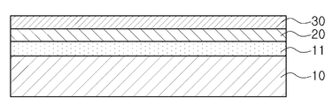
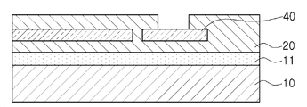
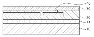
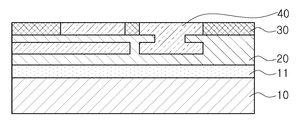
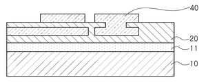
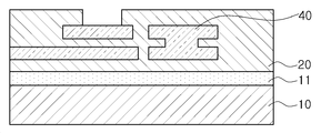
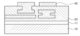
도 2는 도 1b 내지 도 1s의 단계를 반복하여 적층된 바디의 단면도이다.
도 3은 도 2의 바디에 외부전극을 형성한 인덕터의 단면도이다.
140: 코일부 141: 도전성 패턴
142: 도전성 비아
131, 132: 외부전극
Claims (9)
- 지지 부재 상에 패시베이션층(Passivation layer, PSV)을 도포하는 단계;
상기 패시베이션층 상에 DFR(Dry Film Resist)을 라미네이션하는 단계;
상기 DFR(Dry Film Resist)을 노광 및 현상하여 드라이 필름 패턴(Dry Film Pattern)을 형성하는 단계;
상기 드라이 필름 패턴(Dry Film Pattern) 상에 금속 페이스트를 인쇄하여 코일 패턴을 형성하는 단계;
상기 DFR(Dry Film Resist)을 제거하는 단계;
상기 코일 패턴 상에 패시베이션층(Passivation layer, PSV)을 도포하는 단계; 및
상기 패시베이션층(Passivation layer, PSV) 상에 비아를 가공하는 단계;를 포함하는 인덕터의 제조방법.
- 제 1항에 있어서,
상기 비아를 가공하는 단계 이후에,
상기 패시베이션층 상에 DFR(Dry Film Resist)을 라미네이션하는 단계;
상기 DFR(Dry Film Resist)을 노광 및 현상하여 드라이 필름 패턴(Dry Film Pattern)을 형성하는 단계;
상기 드라이 필름 패턴(Dry Film Pattern) 상에 금속 페이스트를 인쇄하여 코일 패턴을 형성하는 단계;
상기 DFR(Dry Film Resist)을 제거하는 단계; 및
상기 코일 패턴 상에 패시베이션층(Passivation layer, PSV)을 도포하는 단계;를 반복하여 적층체를 형성하는 인덕터의 제조방법.
- 제 2항에 있어서,
상기 코일 패턴 상에 패시베이션층(Passivation layer, PSV)을 도포하는 단계 이후에 적층체를 절단하고 소결하는 단계를 더 수행하는 인덕터의 제조방법.
- 제 3항에 있어서,
상기 적층체에서 지지 부재를 제거하고, 적층체의 외측에 외부전극을 형성하는 단계를 더 수행하는 인덕터의 제조방법.
- 제 1항에 있어서,
상기 금속 페이스트는 감광성 금속 페이스트 대비 저항이 낮은 인덕터의 제조방법.
- 제 1항에 있어서,
상기 비아를 가공하는 단계는 패시베이션층(Passivation layer, PSV)을 노광 및 현상하여 수행되는 인덕터의 제조방법.
- 제 1항에 있어서,
상기 드라이 필름 패턴(Dry Film Pattern) 상에 형성된 코일 패턴들은 상기 비아에 의해 서로 연결되는 인덕터의 제조방법.
- 코일부를 포함하는 바디와 상기 바디의 외측에 배치되며, 상기 코일부와 연결된 외부전극을 포함하며,
상기 코일부는 도전성 패턴과 도전성 비아를 가지며, 상기 도전성 패턴과 상기 도전성 비아는 감광성 금속 페이스트에 비해 저항이 낮은 금속 페이스트로 형성된 인덕터.
- 제 8항에 있어서,
상기 도전성 패턴 및 도전성 비아는 은(Ag)을 포함하는 인덕터.
Priority Applications (3)
| Application Number | Priority Date | Filing Date | Title |
|---|---|---|---|
| KR1020160044334A KR20170116499A (ko) | 2016-04-11 | 2016-04-11 | 인덕터 제조방법 및 인덕터 |
| JP2017066283A JP2017191931A (ja) | 2016-04-11 | 2017-03-29 | インダクターの製造方法及びインダクター |
| US15/474,710 US20170294262A1 (en) | 2016-04-11 | 2017-03-30 | Method of manufacturing inductor and inductor |
Applications Claiming Priority (1)
| Application Number | Priority Date | Filing Date | Title |
|---|---|---|---|
| KR1020160044334A KR20170116499A (ko) | 2016-04-11 | 2016-04-11 | 인덕터 제조방법 및 인덕터 |
Publications (1)
| Publication Number | Publication Date |
|---|---|
| KR20170116499A true KR20170116499A (ko) | 2017-10-19 |
Family
ID=59999709
Family Applications (1)
| Application Number | Title | Priority Date | Filing Date |
|---|---|---|---|
| KR1020160044334A Ceased KR20170116499A (ko) | 2016-04-11 | 2016-04-11 | 인덕터 제조방법 및 인덕터 |
Country Status (3)
| Country | Link |
|---|---|
| US (1) | US20170294262A1 (ko) |
| JP (1) | JP2017191931A (ko) |
| KR (1) | KR20170116499A (ko) |
Families Citing this family (2)
| Publication number | Priority date | Publication date | Assignee | Title |
|---|---|---|---|---|
| JP6658681B2 (ja) * | 2017-06-22 | 2020-03-04 | 株式会社村田製作所 | 積層インダクタの製造方法および積層インダクタ |
| JP7266996B2 (ja) * | 2018-11-20 | 2023-05-01 | 太陽誘電株式会社 | インダクタ、フィルタおよびマルチプレクサ |
Family Cites Families (8)
| Publication number | Priority date | Publication date | Assignee | Title |
|---|---|---|---|---|
| JP2002249890A (ja) * | 2001-02-22 | 2002-09-06 | Nikon Corp | コイルの製造方法 |
| JP3754011B2 (ja) * | 2002-09-04 | 2006-03-08 | デプト株式会社 | 電子部品用金属材料、電子部品、電子機器、金属材料の加工方法、電子部品の製造方法及び電子光学部品 |
| US7056817B2 (en) * | 2002-11-20 | 2006-06-06 | Intel Corporation | Forming a cap above a metal layer |
| KR100665114B1 (ko) * | 2005-01-07 | 2007-01-09 | 삼성전기주식회사 | 평면형 자성 인덕터의 제조 방법 |
| CA2701412C (en) * | 2007-10-01 | 2017-06-20 | Kovio, Inc. | Profile engineered thin film devices and structures |
| KR20130058340A (ko) * | 2011-11-25 | 2013-06-04 | 삼성전기주식회사 | 인덕터 및 그 제조 방법 |
| KR101862409B1 (ko) * | 2011-12-22 | 2018-07-05 | 삼성전기주식회사 | 칩 인덕터 및 칩 인덕터 제조방법 |
| KR101973410B1 (ko) * | 2013-08-14 | 2019-09-02 | 삼성전기주식회사 | 박막 인덕터용 코일 유닛, 박막 인덕터용 코일 유닛의 제조방법, 박막 인덕터 및 박막 인덕터의 제조방법 |
-
2016
- 2016-04-11 KR KR1020160044334A patent/KR20170116499A/ko not_active Ceased
-
2017
- 2017-03-29 JP JP2017066283A patent/JP2017191931A/ja active Pending
- 2017-03-30 US US15/474,710 patent/US20170294262A1/en not_active Abandoned
Also Published As
| Publication number | Publication date |
|---|---|
| JP2017191931A (ja) | 2017-10-19 |
| US20170294262A1 (en) | 2017-10-12 |
Similar Documents
| Publication | Publication Date | Title |
|---|---|---|
| US12183501B2 (en) | Inductor component | |
| US9691539B2 (en) | Coil component | |
| KR101565700B1 (ko) | 칩 전자부품, 이의 제조방법 및 그 실장기판 | |
| KR102025708B1 (ko) | 칩 전자부품 및 그 실장기판 | |
| US10147533B2 (en) | Inductor | |
| KR101548862B1 (ko) | 칩형 코일 부품 및 그 제조 방법 | |
| US10418167B2 (en) | Inductor component | |
| US9331009B2 (en) | Chip electronic component and method of manufacturing the same | |
| US10115521B2 (en) | Manufacturing method for electronic component | |
| KR101740816B1 (ko) | 칩 인덕터 | |
| US9401242B2 (en) | Composite electronic component and composite electronic component manufacturing method | |
| US10224389B2 (en) | Embedded passive chip device and method of making the same | |
| JP2005045103A (ja) | チップインダクタ | |
| KR20170116499A (ko) | 인덕터 제조방법 및 인덕터 | |
| WO2004021374A1 (ja) | 可変インダクタンス素子、可変インダクタンス素子内蔵多層基板、半導体チップ及びチップ型可変インダクタンス素子 | |
| JP2012015291A (ja) | コイル装置の製造方法 | |
| KR102154199B1 (ko) | 칩 전자부품 및 그 실장기판 | |
| JP2002100520A (ja) | 積層インダクタ及びそのインダクタンス値の調整方法 | |
| JP4577479B2 (ja) | 多層配線基板形成に用いられる異材質部を有するシート形成方法および異材質部を有するシート | |
| KR100547168B1 (ko) | 적층형 발룬 트랜스포머의 제조 방법 | |
| KR20030092379A (ko) | 내장형 캐패시터를 갖는 세라믹 적층 소자의 제조방법 | |
| WO2019088253A1 (ja) | Lc共振アンテナ | |
| JP2004221330A (ja) | 電子回路基板及びその製造方法 |
Legal Events
| Date | Code | Title | Description |
|---|---|---|---|
| PA0109 | Patent application |
Patent event code: PA01091R01D Comment text: Patent Application Patent event date: 20160411 |
|
| PG1501 | Laying open of application | ||
| A201 | Request for examination | ||
| PA0201 | Request for examination |
Patent event code: PA02012R01D Patent event date: 20210324 Comment text: Request for Examination of Application Patent event code: PA02011R01I Patent event date: 20160411 Comment text: Patent Application |
|
| E902 | Notification of reason for refusal | ||
| PE0902 | Notice of grounds for rejection |
Comment text: Notification of reason for refusal Patent event date: 20220209 Patent event code: PE09021S01D |
|
| AMND | Amendment | ||
| E601 | Decision to refuse application | ||
| PE0601 | Decision on rejection of patent |
Patent event date: 20220415 Comment text: Decision to Refuse Application Patent event code: PE06012S01D Patent event date: 20220209 Comment text: Notification of reason for refusal Patent event code: PE06011S01I |
|
| X091 | Application refused [patent] | ||
| AMND | Amendment | ||
| PX0901 | Re-examination |
Patent event code: PX09011S01I Patent event date: 20220415 Comment text: Decision to Refuse Application Patent event code: PX09012R01I Patent event date: 20220311 Comment text: Amendment to Specification, etc. |
|
| E90F | Notification of reason for final refusal | ||
| PE0902 | Notice of grounds for rejection |
Comment text: Final Notice of Reason for Refusal Patent event date: 20220506 Patent event code: PE09021S02D |
|
| PX0601 | Decision of rejection after re-examination |
Comment text: Decision to Refuse Application Patent event code: PX06014S01D Patent event date: 20220713 Comment text: Final Notice of Reason for Refusal Patent event code: PX06013S02I Patent event date: 20220506 Comment text: Amendment to Specification, etc. Patent event code: PX06012R01I Patent event date: 20220428 Comment text: Decision to Refuse Application Patent event code: PX06011S01I Patent event date: 20220415 Comment text: Amendment to Specification, etc. Patent event code: PX06012R01I Patent event date: 20220311 Comment text: Notification of reason for refusal Patent event code: PX06013S01I Patent event date: 20220209 |
|
| X601 | Decision of rejection after re-examination |