KR20170121082A - 반도체 강유전체 기억소자의 제조방법 및 반도체 강유전체 기억 트랜지스터 - Google Patents
반도체 강유전체 기억소자의 제조방법 및 반도체 강유전체 기억 트랜지스터 Download PDFInfo
- Publication number
- KR20170121082A KR20170121082A KR1020170051593A KR20170051593A KR20170121082A KR 20170121082 A KR20170121082 A KR 20170121082A KR 1020170051593 A KR1020170051593 A KR 1020170051593A KR 20170051593 A KR20170051593 A KR 20170051593A KR 20170121082 A KR20170121082 A KR 20170121082A
- Authority
- KR
- South Korea
- Prior art keywords
- ferroelectric
- oxygen
- annealing
- metal
- bismuth
- Prior art date
- Legal status (The legal status is an assumption and is not a legal conclusion. Google has not performed a legal analysis and makes no representation as to the accuracy of the status listed.)
- Granted
Links
Images











Classifications
-
- H01L29/6684—
-
- H—ELECTRICITY
- H10—SEMICONDUCTOR DEVICES; ELECTRIC SOLID-STATE DEVICES NOT OTHERWISE PROVIDED FOR
- H10D—INORGANIC ELECTRIC SEMICONDUCTOR DEVICES
- H10D64/00—Electrodes of devices having potential barriers
- H10D64/01—Manufacture or treatment
- H10D64/031—Manufacture or treatment of data-storage electrodes
- H10D64/033—Manufacture or treatment of data-storage electrodes comprising ferroelectric layers
-
- H—ELECTRICITY
- H10—SEMICONDUCTOR DEVICES; ELECTRIC SOLID-STATE DEVICES NOT OTHERWISE PROVIDED FOR
- H10B—ELECTRONIC MEMORY DEVICES
- H10B53/00—Ferroelectric RAM [FeRAM] devices comprising ferroelectric memory capacitors
-
- G—PHYSICS
- G11—INFORMATION STORAGE
- G11C—STATIC STORES
- G11C11/00—Digital stores characterised by the use of particular electric or magnetic storage elements; Storage elements therefor
- G11C11/21—Digital stores characterised by the use of particular electric or magnetic storage elements; Storage elements therefor using electric elements
- G11C11/22—Digital stores characterised by the use of particular electric or magnetic storage elements; Storage elements therefor using electric elements using ferroelectric elements
- G11C11/223—Digital stores characterised by the use of particular electric or magnetic storage elements; Storage elements therefor using electric elements using ferroelectric elements using MOS with ferroelectric gate insulating film
-
- H01L21/02181—
-
- H01L21/02197—
-
- H01L21/02337—
-
- H01L21/02356—
-
- H01L21/28291—
-
- H01L29/516—
-
- H01L29/78391—
-
- H—ELECTRICITY
- H10—SEMICONDUCTOR DEVICES; ELECTRIC SOLID-STATE DEVICES NOT OTHERWISE PROVIDED FOR
- H10B—ELECTRONIC MEMORY DEVICES
- H10B53/00—Ferroelectric RAM [FeRAM] devices comprising ferroelectric memory capacitors
- H10B53/30—Ferroelectric RAM [FeRAM] devices comprising ferroelectric memory capacitors characterised by the memory core region
-
- H—ELECTRICITY
- H10—SEMICONDUCTOR DEVICES; ELECTRIC SOLID-STATE DEVICES NOT OTHERWISE PROVIDED FOR
- H10D—INORGANIC ELECTRIC SEMICONDUCTOR DEVICES
- H10D30/00—Field-effect transistors [FET]
- H10D30/01—Manufacture or treatment
- H10D30/021—Manufacture or treatment of FETs having insulated gates [IGFET]
- H10D30/0415—Manufacture or treatment of FETs having insulated gates [IGFET] of FETs having ferroelectric gate insulators
-
- H—ELECTRICITY
- H10—SEMICONDUCTOR DEVICES; ELECTRIC SOLID-STATE DEVICES NOT OTHERWISE PROVIDED FOR
- H10D—INORGANIC ELECTRIC SEMICONDUCTOR DEVICES
- H10D30/00—Field-effect transistors [FET]
- H10D30/60—Insulated-gate field-effect transistors [IGFET]
- H10D30/701—IGFETs having ferroelectric gate insulators, e.g. ferroelectric FETs
-
- H—ELECTRICITY
- H10—SEMICONDUCTOR DEVICES; ELECTRIC SOLID-STATE DEVICES NOT OTHERWISE PROVIDED FOR
- H10D—INORGANIC ELECTRIC SEMICONDUCTOR DEVICES
- H10D64/00—Electrodes of devices having potential barriers
- H10D64/60—Electrodes characterised by their materials
- H10D64/66—Electrodes having a conductor capacitively coupled to a semiconductor by an insulator, e.g. MIS electrodes
- H10D64/68—Electrodes having a conductor capacitively coupled to a semiconductor by an insulator, e.g. MIS electrodes characterised by the insulator, e.g. by the gate insulator
- H10D64/681—Electrodes having a conductor capacitively coupled to a semiconductor by an insulator, e.g. MIS electrodes characterised by the insulator, e.g. by the gate insulator having a compositional variation, e.g. multilayered
- H10D64/685—Electrodes having a conductor capacitively coupled to a semiconductor by an insulator, e.g. MIS electrodes characterised by the insulator, e.g. by the gate insulator having a compositional variation, e.g. multilayered being perpendicular to the channel plane
-
- H—ELECTRICITY
- H10—SEMICONDUCTOR DEVICES; ELECTRIC SOLID-STATE DEVICES NOT OTHERWISE PROVIDED FOR
- H10D—INORGANIC ELECTRIC SEMICONDUCTOR DEVICES
- H10D64/00—Electrodes of devices having potential barriers
- H10D64/60—Electrodes characterised by their materials
- H10D64/66—Electrodes having a conductor capacitively coupled to a semiconductor by an insulator, e.g. MIS electrodes
- H10D64/68—Electrodes having a conductor capacitively coupled to a semiconductor by an insulator, e.g. MIS electrodes characterised by the insulator, e.g. by the gate insulator
- H10D64/689—Electrodes having a conductor capacitively coupled to a semiconductor by an insulator, e.g. MIS electrodes characterised by the insulator, e.g. by the gate insulator having ferroelectric layers
-
- H—ELECTRICITY
- H10—SEMICONDUCTOR DEVICES; ELECTRIC SOLID-STATE DEVICES NOT OTHERWISE PROVIDED FOR
- H10P—GENERIC PROCESSES OR APPARATUS FOR THE MANUFACTURE OR TREATMENT OF DEVICES COVERED BY CLASS H10
- H10P14/00—Formation of materials, e.g. in the shape of layers or pillars
- H10P14/60—Formation of materials, e.g. in the shape of layers or pillars of insulating materials
- H10P14/63—Formation of materials, e.g. in the shape of layers or pillars of insulating materials characterised by the formation processes
- H10P14/6326—Deposition processes
- H10P14/6328—Deposition from the gas or vapour phase
- H10P14/6329—Deposition from the gas or vapour phase using physical ablation of a target, e.g. physical vapour deposition or pulsed laser deposition
-
- H—ELECTRICITY
- H10—SEMICONDUCTOR DEVICES; ELECTRIC SOLID-STATE DEVICES NOT OTHERWISE PROVIDED FOR
- H10P—GENERIC PROCESSES OR APPARATUS FOR THE MANUFACTURE OR TREATMENT OF DEVICES COVERED BY CLASS H10
- H10P14/00—Formation of materials, e.g. in the shape of layers or pillars
- H10P14/60—Formation of materials, e.g. in the shape of layers or pillars of insulating materials
- H10P14/63—Formation of materials, e.g. in the shape of layers or pillars of insulating materials characterised by the formation processes
- H10P14/6326—Deposition processes
- H10P14/6328—Deposition from the gas or vapour phase
- H10P14/6334—Deposition from the gas or vapour phase using decomposition or reaction of gaseous or vapour phase compounds, i.e. chemical vapour deposition
-
- H—ELECTRICITY
- H10—SEMICONDUCTOR DEVICES; ELECTRIC SOLID-STATE DEVICES NOT OTHERWISE PROVIDED FOR
- H10P—GENERIC PROCESSES OR APPARATUS FOR THE MANUFACTURE OR TREATMENT OF DEVICES COVERED BY CLASS H10
- H10P14/00—Formation of materials, e.g. in the shape of layers or pillars
- H10P14/60—Formation of materials, e.g. in the shape of layers or pillars of insulating materials
- H10P14/65—Formation of materials, e.g. in the shape of layers or pillars of insulating materials characterised by treatments performed before or after the formation of the materials
- H10P14/6516—Formation of materials, e.g. in the shape of layers or pillars of insulating materials characterised by treatments performed before or after the formation of the materials of treatments performed after formation of the materials
- H10P14/6529—Formation of materials, e.g. in the shape of layers or pillars of insulating materials characterised by treatments performed before or after the formation of the materials of treatments performed after formation of the materials by exposure to a gas or vapour
-
- H—ELECTRICITY
- H10—SEMICONDUCTOR DEVICES; ELECTRIC SOLID-STATE DEVICES NOT OTHERWISE PROVIDED FOR
- H10P—GENERIC PROCESSES OR APPARATUS FOR THE MANUFACTURE OR TREATMENT OF DEVICES COVERED BY CLASS H10
- H10P14/00—Formation of materials, e.g. in the shape of layers or pillars
- H10P14/60—Formation of materials, e.g. in the shape of layers or pillars of insulating materials
- H10P14/65—Formation of materials, e.g. in the shape of layers or pillars of insulating materials characterised by treatments performed before or after the formation of the materials
- H10P14/6516—Formation of materials, e.g. in the shape of layers or pillars of insulating materials characterised by treatments performed before or after the formation of the materials of treatments performed after formation of the materials
- H10P14/6544—Formation of materials, e.g. in the shape of layers or pillars of insulating materials characterised by treatments performed before or after the formation of the materials of treatments performed after formation of the materials to change the morphology of the insulating materials, e.g. transformation of an amorphous layer into a crystalline layer
-
- H—ELECTRICITY
- H10—SEMICONDUCTOR DEVICES; ELECTRIC SOLID-STATE DEVICES NOT OTHERWISE PROVIDED FOR
- H10P—GENERIC PROCESSES OR APPARATUS FOR THE MANUFACTURE OR TREATMENT OF DEVICES COVERED BY CLASS H10
- H10P14/00—Formation of materials, e.g. in the shape of layers or pillars
- H10P14/60—Formation of materials, e.g. in the shape of layers or pillars of insulating materials
- H10P14/66—Formation of materials, e.g. in the shape of layers or pillars of insulating materials characterised by the type of materials
- H10P14/662—Laminate layers, e.g. stacks of alternating high-k metal oxides
-
- H—ELECTRICITY
- H10—SEMICONDUCTOR DEVICES; ELECTRIC SOLID-STATE DEVICES NOT OTHERWISE PROVIDED FOR
- H10P—GENERIC PROCESSES OR APPARATUS FOR THE MANUFACTURE OR TREATMENT OF DEVICES COVERED BY CLASS H10
- H10P14/00—Formation of materials, e.g. in the shape of layers or pillars
- H10P14/60—Formation of materials, e.g. in the shape of layers or pillars of insulating materials
- H10P14/69—Inorganic materials
- H10P14/692—Inorganic materials composed of oxides, glassy oxides or oxide-based glasses
- H10P14/6938—Inorganic materials composed of oxides, glassy oxides or oxide-based glasses the material containing at least one metal element, e.g. metal oxides, metal oxynitrides or metal oxycarbides
- H10P14/6939—Inorganic materials composed of oxides, glassy oxides or oxide-based glasses the material containing at least one metal element, e.g. metal oxides, metal oxynitrides or metal oxycarbides characterised by the metal
- H10P14/69392—Inorganic materials composed of oxides, glassy oxides or oxide-based glasses the material containing at least one metal element, e.g. metal oxides, metal oxynitrides or metal oxycarbides characterised by the metal the material containing hafnium, e.g. HfO2
-
- H—ELECTRICITY
- H10—SEMICONDUCTOR DEVICES; ELECTRIC SOLID-STATE DEVICES NOT OTHERWISE PROVIDED FOR
- H10P—GENERIC PROCESSES OR APPARATUS FOR THE MANUFACTURE OR TREATMENT OF DEVICES COVERED BY CLASS H10
- H10P14/00—Formation of materials, e.g. in the shape of layers or pillars
- H10P14/60—Formation of materials, e.g. in the shape of layers or pillars of insulating materials
- H10P14/69—Inorganic materials
- H10P14/692—Inorganic materials composed of oxides, glassy oxides or oxide-based glasses
- H10P14/6938—Inorganic materials composed of oxides, glassy oxides or oxide-based glasses the material containing at least one metal element, e.g. metal oxides, metal oxynitrides or metal oxycarbides
- H10P14/69398—Inorganic materials composed of oxides, glassy oxides or oxide-based glasses the material containing at least one metal element, e.g. metal oxides, metal oxynitrides or metal oxycarbides the material having a perovskite structure, e.g. BaTiO3
-
- H—ELECTRICITY
- H10—SEMICONDUCTOR DEVICES; ELECTRIC SOLID-STATE DEVICES NOT OTHERWISE PROVIDED FOR
- H10B—ELECTRONIC MEMORY DEVICES
- H10B51/00—Ferroelectric RAM [FeRAM] devices comprising ferroelectric memory transistors
- H10B51/30—Ferroelectric RAM [FeRAM] devices comprising ferroelectric memory transistors characterised by the memory core region
-
- H—ELECTRICITY
- H10—SEMICONDUCTOR DEVICES; ELECTRIC SOLID-STATE DEVICES NOT OTHERWISE PROVIDED FOR
- H10D—INORGANIC ELECTRIC SEMICONDUCTOR DEVICES
- H10D64/00—Electrodes of devices having potential barriers
- H10D64/60—Electrodes characterised by their materials
- H10D64/66—Electrodes having a conductor capacitively coupled to a semiconductor by an insulator, e.g. MIS electrodes
- H10D64/665—Electrodes having a conductor capacitively coupled to a semiconductor by an insulator, e.g. MIS electrodes the conductor comprising a layer of elemental metal contacting the insulator, e.g. tungsten or molybdenum
-
- H—ELECTRICITY
- H10—SEMICONDUCTOR DEVICES; ELECTRIC SOLID-STATE DEVICES NOT OTHERWISE PROVIDED FOR
- H10D—INORGANIC ELECTRIC SEMICONDUCTOR DEVICES
- H10D64/00—Electrodes of devices having potential barriers
- H10D64/60—Electrodes characterised by their materials
- H10D64/66—Electrodes having a conductor capacitively coupled to a semiconductor by an insulator, e.g. MIS electrodes
- H10D64/667—Electrodes having a conductor capacitively coupled to a semiconductor by an insulator, e.g. MIS electrodes the conductor comprising a layer of alloy material, compound material or organic material contacting the insulator, e.g. TiN workfunction layers
-
- H—ELECTRICITY
- H10—SEMICONDUCTOR DEVICES; ELECTRIC SOLID-STATE DEVICES NOT OTHERWISE PROVIDED FOR
- H10D—INORGANIC ELECTRIC SEMICONDUCTOR DEVICES
- H10D64/00—Electrodes of devices having potential barriers
- H10D64/60—Electrodes characterised by their materials
- H10D64/66—Electrodes having a conductor capacitively coupled to a semiconductor by an insulator, e.g. MIS electrodes
- H10D64/68—Electrodes having a conductor capacitively coupled to a semiconductor by an insulator, e.g. MIS electrodes characterised by the insulator, e.g. by the gate insulator
- H10D64/691—Electrodes having a conductor capacitively coupled to a semiconductor by an insulator, e.g. MIS electrodes characterised by the insulator, e.g. by the gate insulator comprising metallic compounds, e.g. metal oxides or metal silicates
-
- H—ELECTRICITY
- H10—SEMICONDUCTOR DEVICES; ELECTRIC SOLID-STATE DEVICES NOT OTHERWISE PROVIDED FOR
- H10D—INORGANIC ELECTRIC SEMICONDUCTOR DEVICES
- H10D64/00—Electrodes of devices having potential barriers
- H10D64/60—Electrodes characterised by their materials
- H10D64/66—Electrodes having a conductor capacitively coupled to a semiconductor by an insulator, e.g. MIS electrodes
- H10D64/68—Electrodes having a conductor capacitively coupled to a semiconductor by an insulator, e.g. MIS electrodes characterised by the insulator, e.g. by the gate insulator
- H10D64/693—Electrodes having a conductor capacitively coupled to a semiconductor by an insulator, e.g. MIS electrodes characterised by the insulator, e.g. by the gate insulator the insulator comprising nitrogen, e.g. nitrides, oxynitrides or nitrogen-doped materials
Landscapes
- Engineering & Computer Science (AREA)
- Computer Hardware Design (AREA)
- Chemical & Material Sciences (AREA)
- Non-Volatile Memory (AREA)
- Semiconductor Memories (AREA)
- Materials Engineering (AREA)
- Crystallography & Structural Chemistry (AREA)
- Chemical Kinetics & Catalysis (AREA)
- Physics & Mathematics (AREA)
- Optics & Photonics (AREA)
- Formation Of Insulating Films (AREA)
Abstract
Description
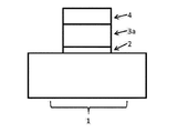
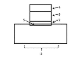
도 2는 본 발명의 제2 실시형태의 반도체 강유전체 기억소자의 제작 도중을 나타내는 단면도이다.
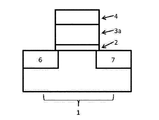
도 3은 본 발명의 제1 실시형태의 반도체 강유전체 기억소자의 단면도이다.
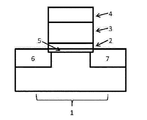
도 4는 본 발명의 제2 실시형태의 반도체 강유전체 기억소자의 단면도이다.
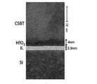
도 5는 실시예 02B의 단면 TEM 사진이다.
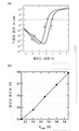
도 6은 실시예 02B의 (a) FeFET의 드레인 전류와 게이트 전압의 관계를 나타내는 그래프와, (b) 소인진폭 Vamp와 메모리 윈도우의 관계를 나타내는 그래프이다.
도 7은 실시예 21C의 단면 TEM 사진이다.
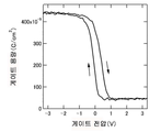
도 8은 실시예 02A의 금속과 반도체 기체 사이의 게이트 전압에 대한 전기용량의 관계이다.
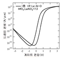
도 9는 게이트 적층의 구조와 두께가 Ir(75nm)/CSBT(x=0.2,135nm)/Hf-La-Al-O(5nm)/Si인 실시예 26C의 드레인 전류와 게이트 전압의 관계이다. 절연체(5)(I층)의 조성비는 HfO2:LaAlO3=7:3이다.
도 10은 게이트 적층의 구조와 두께가 Ir(75nm)/CSBT(x=0.25,135nm)/Zr-Y-O(5nm)/Si인 실시예 16A의 드레인 전류와 게이트 전압의 관계를 나타내는 그래프이다. 절연체(5)(I층)는 Zr-Y-O이다.
도 11은 게이트 적층의 구조와 두께가 Ir(75nm)/CSBT(x=0.2,135nm)/HfO2(4nm)/Si인 실시예 302B의 드레인 전류와 게이트 전압의 관계를 나타내는 그래프이다.
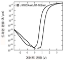
도 12는 게이트 적층의 구조와 두께가 Ir(75nm)/CSBT(x=0.2,135nm)/HfO2(4nm)/Hf-N(2nm)/Si인 실시예 12B의 드레인 전류와 게이트 전압의 관계를 나타내는 그래프이다.
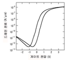
도 13은 게이트 적층의 구조와 두께가 Ir(75nm)/CSBT(x=0.15,120nm)/HfO2(5nm)/Si인 실시예 09F의 드레인 전류와 게이트 전압의 관계를 나타내는 그래프이다.
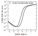
도 14는 게이트 적층의 구조와 두께가 Ir(75nm)/CSBT(x=0.2,135nm)/Hf-Mg-O(5nm)/Si인 실시예 03C의 드레인 전류와 게이트 전압의 관계를 나타내는 그래프이다. Ar-O2 중에서 결정화 어닐링을 실시한다.
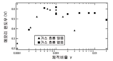
도 15는 강유전체 결정 어닐링시의 N2에 대한 O2의 체적비율 y와, 그 적층비율을 이용하여 제조하여 금속(4)이 Ir인 실시예 FeFET의 Id-Vg 특성의 메모리 윈도우와의 관계를 나타내는 그래프이다.
도 16은 강유전체 결정화 어닐링의 공정에 있어서의 어닐링 온도와 제조한 FeFET의 Id-Vg 특성의 메모리 윈도우의 관계를 나타내는 그래프이다.
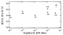
도 17은 1기압보다 작은 감압환경에서의 강유전체 결정화 어닐링도 행한 실시예의 정리도이다.
도 18은 절연체(2)에 HfO2를 채용한 경우의 HfO2의 두께와 메모리 윈도우의 관계를 나타내는 그래프이다.
도 19는 실시예 02B에 대하여 제1 방법의 특성 조정 어닐링을 행하기 전과 행한 후의 Id-Vg 특성을 나타내는 그래프이다.
도 20은 제1 방법의 어닐링 온도와 메모리 윈도우 변화율 및 SS값의 변화율의 관계를 나타내는 그래프이다.
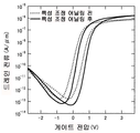
도 21은 실시예 21C를 400℃에서 30분간 제2 방법의 특성 조정 어닐링을 행한 후(실선커브)와 행하기 전(점선커브)의 드레인 전류와 게이트 전압의 관계를 나타내는 그래프이다.
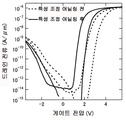
도 22는 실시예 23C를 400℃에서 5분간 제2 방법의 특성 조정 어닐링을 행한 후(실선커브)와 행하기 전(점선커브)의 드레인 전류와 게이트 전압의 관계를 나타내는 그래프이다.
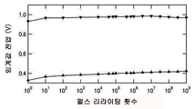
도 23은 실시예 02B에 대한 데이터 리라이팅 내성 시험의 결과를 나타내는 그래프이다. 입력 펄스는 -3.3V와 +3.3V의 교류 펄스이다.
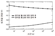
도 24는 실시예 02B에 대한 데이터 보유 특성 측정 결과를 나타내는 그래프이다(입력 전압은 ±3.3V).
도 25는 실시예 27E에 대한 데이터 리라이팅 내성 시험 결과를 나타내는 그래프이다.
도 26은 실시예 12H에 대한 데이터 리라이팅 내성 시험 결과를 나타내는 그래프이다.
도 27은 실시예 27F에 대한 데이터 보유 특성 측정 결과를 나타내는 그래프이다.
도 28은 실시예 12H에 대한 데이터 보유 특성 측정 결과를 나타내는 그래프이다.
도 29는 실시예 302B의 제조 과정의 설명도이다.
도 30은 선행기술에서 제작한 FeFET의 드레인 전류-게이트 전압의 관계를 나타내는 그래프: (a) 강유전체 Ca0 . 2Sr0 . 8Bi2Ta2O9의 막두께 120nm의 FeFET의 특성과, (b) Ca0 . 2Sr0 . 8Bi2Ta2O9의 막두께 160nm의 FeFET의 특성이다. (c) 막두께 120nm, 160nm, 200nm의 Ca0 . 2Sr0 . 8Bi2Ta2O9을 강유전체로 하는 선행기술로 제작한 FeFET의 메모리 윈도우와 강유전체의 막두께와의 관계를 나타내는 그래프이다. ○표시는 산소 중 775℃와 ●표시는 산소 중 800℃에서 30분 어닐링을 행하였다. 메모리 윈도우를 얻기 위한 게이트 전압 소인범위는, 0.5V±3.3V이다. (d) 소인진폭 3.3V와 5.0V에 대한 메모리 윈도우이다.
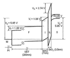
도 31은 데이터 입력을 위한 양의 전압이 Pt/SrBi2Ta2O9/Hf-Al-O/Si의 FeFET의 게이트에 가해졌을 때의 게이트 각 부분에 걸리는 전압분할과 게이트 깊이 방향의 에너지대 다이어그램이다.
2: 절연체
3a: 막
3: 강유전체
4: 금속
5: SiO2를 주성분으로 하는 계면층(IL)
6. 소스 영역
7. 드레인 영역
| 실시예명칭 | Hf-N의 제조조건 | HfO2 두께 (nm) | CSBT (x=0.2) 두께 (nm) | 강유전체 결정화 어닐링 | 메모리 윈도우 (V) | ||||
| NH3 유량 (sccm) | 서셉터 온도 (℃) | 두께 (nm) | 가스 흐름 유무 | 산소체적 비율 y | 온도 (℃) | ||||
| 11A | 9 | 260 | 1 | 3 | 135 | 없음 | 0.001 | 780 | 0.54 |
| 11B | 9 | 260 | 1 | 3 | 135 | 없음 | 0.001 | 780 | 0.47 |
| 11C | 9 | 260 | 1.5 | 3 | 135 | 없음 | 0.001 | 780 | 0.51 |
| 11D | 9 | 260 | 1.5 | 4 | 135 | 없음 | 0.0005 | 780 | 0.42 |
| 12A | 9 | 260 | 2 | 3 | 135 | 없음 | 0.001 | 780 | 0.5 |
| 12B | 9 | 260 | 2 | 4 | 135 | 없음 | 0.001 | 780 | 0.57 |
| 04A | 20 | 260 | 1 | 3 | 135 | 없음 | 0.001 | 780 | 0.53 |
| 04B | 20 | 260 | 1 | 4 | 135 | 없음 | 0.0005 | 780 | 0.54 |
| 04C | 20 | 260 | 1.5 | 3 | 135 | 없음 | 0.001 | 780 | 0.53 |
| 05A | 20 | 260 | 2 | 4 | 135 | 없음 | 0.001 | 780 | 0.56 |
| 23A | 20 | 400 | 1 | 4 | 135 | 없음 | 0.001 | 780 | 0.47 |
| 24A | 20 | 400 | 1.5 | 4 | 135 | 없음 | 0.001 | 780 | 0.43 |
| 실시예 명칭 | I층 HfO2 두께 (nm) | F층 CSBT (x=0.2) 두께(nm) | M층 Ir 두께 (nm) | 어닐링시의 온도 Tan (℃) | 어닐링시의 가스 흐름 | 어닐링시의 산소체적비율 (대질소) | 어닐링시의 압력 (MPa) | 메모리 윈도우 (V) |
| 12G | 5 | 135 | 75 | 750 | 있음 | 0.001 | 0.04 | 0.44 |
| 12H | 5 | 135 | 75 | 750 | 있음 | 0.001 | 0.01 | 0.45 |
| 12I | 5 | 135 | 75 | 750 | 있음 | 0.001 | 0.001 | 0.40 |
| 21B | 4 | 135 | 75 | 780 | 있음 | 0.001 | 0.01 | 0.51 |
| 16F | 4 | 135 | 75 | 780 | 없음 | 0.001 | 0.0475 | 0.54 |
| 실시예 명칭 | I층 HfO2 두께 (nm) | F층 CSBT (x=0.2) 두께(nm) | M층 Ir 두께 (nm) | 어닐링시의 온도 Tan (℃) | 어닐링시의 가스 흐름 | 어닐링시의 산소유량 (sccm) | 어닐링시의 압력 (Pa) | 메모리 윈도우 (V) |
| 12K | 5 | 135 | 75 | 750 | 있음 | 3 | 100 | 0.47 |
| 12L | 5 | 135 | 75 | 750 | 있음 | 3 | 10 | 0.4 |
| 실시예 명칭 | 절연체 | 강유전체 | 금속 | 강유전체 결정화 어닐링 | 메모리 윈도우 (V) | ||||
| HfO2 두께 (nm) | CSBT x=0.2 (nm) | 재료종류 | 제조법 | 두께 (nm) | 가스 흐름 유무 | 산소 체적비율 y | 온도 (℃) | ||
| 22A | 4 | 135 | Pt | 전자빔 증착 | 150 | 있음 | 0.003 | 780 | 0.46 |
| 22B | 4 | 135 | Pt | 전자빔 증착 | 150 | 있음 | 0.006 | 780 | 0.40 |
| 22C | 4 | 135 | Pt | 전자빔 증착 | 150 | 있음 | 0.0007 | 780 | 0.42 |
| 19E | 5 | 135 | Pt | 전자빔 증착 | 150 | 있음 | 0.0003 | 780 | 0.30 |
| 19B | 5 | 135 | Pt | 전자빔 증착 | 150 | 있음 | 0.001 | 780 | 0.49 |
| 19C | 5 | 135 | Pt | 전자빔 증착 | 150 | 있음 | 0.01 | 780 | 0.40 |
| 14A | 4 | 146 | Ir Pt 합금 | 스퍼터링 | 75 | 있음 | 0.0001 | 780 | 0.56 |
| 14B | 4 | 146 | Ir Pt 합금 | 스퍼터링 | 75 | 있음 | 0.0004 | 780 | 0.49 |
| 17C | 4 | 135 | Ru | 스퍼터링 | 70 | 있음 | 0.0005 | 740 | 0.40 |
Claims (22)
- 반도체 기체 상에 절연체와 비스무트 층상 페로브스카이트 결정의 강유전체의 구성 원소로 구성된 막과 금속을 이 순서로 형성한 후에 강유전체 결정화 어닐링을 행하는, 반도체 기체와 절연체와 강유전체와 금속으로 이루어지는 소자의 제조방법으로서,
상기 막은 스트론튬과 비스무트와 탄탈과 산소의 원소로 구성되는 막, 칼슘과 스트론튬과 비스무트와 탄탈과 산소의 막, 스트론튬과 비스무트와 탄탈과 니오브와 산소의 막, 칼슘과 스트론튬과 비스무트와 탄탈과 니오브와 산소의 막이고,
상기 금속은 Ir, 또는 Pt, 또는 Ir과 Pt의 합금, 또는 Ru로 구성하고,
상기 강유전체 결정화 어닐링은, 질소에 산소를 더한 혼합가스 중 또는 아르곤에 산소를 더한 혼합가스 중에서 행하는 것을 특징으로 하는 반도체 강유전체 기억소자의 제조방법. - 제 1 항에 있어서,
상기 반도체 기체가 소스 영역과 드레인 영역을 가지고, 상기 반도체 강유전체 기억소자가 트랜지스터인 것을 특징으로 하는 반도체 강유전체 기억소자의 제조방법. - 제 1 항 및 제 2 항에 있어서,
상기 강유전체 결정화 어닐링의 온도가 730℃ 이상 800℃ 이하인 것을 특징으로 하는 반도체 강유전체 기억소자의 제조방법. - 제 1 항 및 제 2 항에 있어서,
상기 금속이 Ir이고, 또한 상기 질소에 산소를 더한 혼합가스의 산소의 질소에 대한 체적비율이 0.0002 이상 0.02 이하인 것을 특징으로 하는 반도체 강유전체 기억소자의 제조방법. - 제 1 항 및 제 2 항에 있어서,
상기 금속이 Pt이고, 또한 상기 질소에 산소를 더한 혼합가스의 산소의 질소에 대한 체적비율이 0.0007보다 크고 0.01 이하인 것을 특징으로 하는 반도체 강유전체 기억소자의 제조방법. - 제 1 항 및 제 2 항에 있어서,
상기 금속이 중량비 1:1의 Ir과 Pt의 합금이고, 또한 상기 질소에 산소를 더한 혼합가스의 산소의 질소에 대한 체적비율이 0.0001보다 크고 0.0004 이하인 것을 특징으로 하는 반도체 강유전체 기억소자의 제조방법. - 제 1 항 및 제 2 항에 있어서,
상기 강유전체 결정화 어닐링시의 압력이 0.001MPa 이상이고, 1기압 이하인 것을 특징으로 하는 반도체 강유전체 기억소자의 제조방법. - 제 1 항 및 제 2 항에 있어서,
상기 절연체가, 하프늄, 지르코늄, 란탄, 이트륨, 알루미늄, 마그네슘, 망간의 금속원소를 적어도 1종류 포함하는 금속산화물, 및 그 금속산화물의 적층금속산화물인 것을 특징으로 하는 반도체 강유전체 기억소자의 제조방법. - 제 1 항 및 제 2 항에 있어서,
상기 절연체가, 질화하프늄 또는 질화알루미늄의 질화물인 것을 특징으로 하는 반도체 강유전체 기억소자의 제조방법. - 제 1 항 및 제 2 항에 있어서,
상기 절연체가, 상기 질화물과 상기 금속산화물, 또는 상기 질화물과 상기 적층금속산화물의 적층인 것을 특징으로 하는 반도체 강유전체 기억소자의 제조방법. - 제 10 항에 있어서,
상기 질화물이 질화하프늄이고, 상기 금속산화물이 HfO2인 것을 특징으로 하는 반도체 강유전체 기억소자의 제조방법. - 제 8 항에 있어서,
상기 금속산화물이 HfO2이고, HfO2의 막두께가 1.3nm 이상 13nm 이하인 것을 특징으로 하는 반도체 강유전체 기억소자의 제조방법. - 제 1 항 및 제 2 항에 있어서,
상기 강유전체 결정화 어닐링을 행한 이후에, 특성 조정 어닐링을 행하고, 그 특성 조정 어닐링은 산소 가스 중에서의 어닐링 또는 질소에 수소를 혼합한 혼합가스에서의 어닐링의 적어도 한쪽 어닐링인 것을 특징으로 하는 반도체 강유전체 기억소자의 제조방법. - 제 13 항에 있어서,
상기 특성 조정 어닐링에 있어서의 상기 산소 가스 중에서의 어닐링의 온도는, 600℃ 이상 700℃ 이하인 것을 특징으로 하는 반도체 강유전체 기억소자의 제조방법. - 제 13 항에 있어서,
상기 특성 조정 어닐링에 있어서의 상기 질소에 수소를 혼합한 혼합가스의 어닐링의 온도는 350℃ 이상 450℃ 이하인 것을 특징으로 하는 반도체 강유전체 기억소자의 제조방법. - 제 13 항에 있어서,
상기 특성 조정 어닐링에 있어서의 상기 질소에 수소를 혼합한 혼합가스의 어닐링의 시간은 3분 이상 30분 이하인 것을 특징으로 하는 반도체 강유전체 기억소자의 제조방법. - 반도체 기체 상에 절연체와 비스무트 층상 페로브스카이트 결정의 강유전체의 구성 원소로 구성된 막과 금속을 이 순서로 형성한 후에 강유전체 결정화 어닐링을 행하는, 반도체 기체와 절연체와 강유전체와 금속으로 이루어지는 소자의 제조방법으로서,
상기 막은 스트론튬과 비스무트와 탄탈과 산소의 원소로 구성되는 막, 칼슘과 스트론튬과 비스무트와 탄탈과 산소의 막, 스트론튬과 비스무트와 탄탈과 니오브와 산소의 막, 칼슘과 스트론튬과 비스무트와 탄탈과 니오브와 산소의 막이고,
상기 금속은 Ir, 또는 Pt, 또는 Ir과 Pt의 합금, 또는 Ru로 구성하며,
상기 강유전체 결정화 어닐링은, 압력이 10Pa 이상 100Pa 이하의 산소분위기 중에서 행하는 것을 특징으로 하는 반도체 강유전체 기억소자의 제조방법. - 제 9 항에 있어서,
Hf를 포함하는 착체를 용매에 용해한 원료용액을 반송가스 중에 분산한 기액 2상 상태의 원료가스를, 기액 2상 상태를 유지한채로 기화실에 도입하여 기화실에 있어서 기화를 행한 후, 성막실로 도입하는 유기금속 화학기상 퇴적법에 의하여, Hf를 포함하는 착체와 NH3 가스가 성장실에서 반응하여 상기 질화하프늄이 형성되는 것을 특징으로 하는 반도체 강유전체 기억소자의 제조방법. - 제 18 항에 있어서,
상기 하프늄을 포함하는 착체가, TEMAHF 또는 TDEAHF인 것을 특징으로 하는 반도체 강유전체 기억소자의 제조방법. - 소스 영역과 드레인 영역을 가지는 반도체 기체와 절연체와 강유전체와 금속이 이 순서로 적층되고,
상기 강유전체는, 스트론튬과 비스무트와 탄탈과 산소로 구성된 비스무트 층상 페로브스카이트 강유전체, 또는 칼슘과 스트론튬과 비스무트와 탄탈과 산소로 구성된 비스무트 층상 페로브스카이트 강유전체, 또는 스트론튬과 비스무트와 탄탈과 니오브와 산소로 구성된 비스무트 층상 페로브스카이트 강유전체, 또는 칼슘과 스트론튬과 비스무트와 탄탈과 니오브와 산소로 구성된 비스무트 층상 페로브스카이트 강유전체이며,
상기 금속은, Ir, 또는 Pt, 또는 Ir과 Pt의 합금, 또는 Ru이고,
상기 강유전체의 막두께가 59nm보다 크고 150nm보다 작으며, 데이터 입력은 입력 전압의 절대치가 3.3V 이하여도 이용하는 것이 가능한 것을 특징으로 하고, 105초 이상 데이터 보유가 가능한 것을 특징으로 하는 반도체 강유전체 기억 트랜지스터. - 제 20 항에 있어서,
상기 반도체 강유전체 기억 트랜지스터가 108회 이상 데이터 리라이팅 가능한 것을 특징으로 하는 반도체 강유전체 기억 트랜지스터. - 제 20 항에 있어서,
상기 반도체 기체와 상기 절연체의 계면에 형성되는 반도체 기체 표면의 계면층의 두께가 3.4nm보다 작은 것을 특징으로 하는 반도체 강유전체 기억 트랜지스터.
Applications Claiming Priority (2)
| Application Number | Priority Date | Filing Date | Title |
|---|---|---|---|
| JP2016086570A JP6751866B2 (ja) | 2016-04-22 | 2016-04-22 | 半導体強誘電体記憶素子の製造方法及び半導体強誘電体記憶トランジスタ |
| JPJP-P-2016-086570 | 2016-04-22 |
Publications (2)
| Publication Number | Publication Date |
|---|---|
| KR20170121082A true KR20170121082A (ko) | 2017-11-01 |
| KR102154646B1 KR102154646B1 (ko) | 2020-09-10 |
Family
ID=58644838
Family Applications (1)
| Application Number | Title | Priority Date | Filing Date |
|---|---|---|---|
| KR1020170051593A Active KR102154646B1 (ko) | 2016-04-22 | 2017-04-21 | 반도체 강유전체 기억소자의 제조방법 및 반도체 강유전체 기억 트랜지스터 |
Country Status (6)
| Country | Link |
|---|---|
| US (2) | US10686043B2 (ko) |
| EP (1) | EP3236487B1 (ko) |
| JP (1) | JP6751866B2 (ko) |
| KR (1) | KR102154646B1 (ko) |
| CN (1) | CN107452742B (ko) |
| TW (1) | TWI721157B (ko) |
Families Citing this family (14)
| Publication number | Priority date | Publication date | Assignee | Title |
|---|---|---|---|---|
| KR20190008049A (ko) * | 2017-07-14 | 2019-01-23 | 에스케이하이닉스 주식회사 | 강유전성 메모리 소자의 제조 방법 |
| KR20190115508A (ko) * | 2018-03-15 | 2019-10-14 | 에스케이하이닉스 주식회사 | 강유전성 메모리 장치 |
| US10879391B2 (en) | 2019-05-07 | 2020-12-29 | Taiwan Semiconductor Manufacturing Co., Ltd. | Wakeup-free ferroelectric memory device |
| KR102827209B1 (ko) | 2019-07-29 | 2025-07-01 | 삼성전자주식회사 | 반도체 소자 및 그 제조 방법 |
| US11139315B2 (en) * | 2019-10-31 | 2021-10-05 | Qualcomm Incorporated | Ferroelectric transistor |
| US11227933B2 (en) * | 2020-03-31 | 2022-01-18 | Taiwan Semiconductor Manufacturing Company Limited | Ferroelectric field effect transistor using charge trapping band misalignment and methods of forming the same |
| KR102906608B1 (ko) * | 2020-05-19 | 2025-12-30 | 삼성전자주식회사 | 산화물 반도체 트랜지스터 |
| US11569382B2 (en) * | 2020-06-15 | 2023-01-31 | Taiwan Semiconductor Manufacturing Company, Ltd. | Semiconductor device and method of fabricating the same |
| US12148828B2 (en) * | 2020-06-18 | 2024-11-19 | Taiwan Semiconductor Manufacturing Company, Ltd. | Semiconductor device and manufacturing method thereof |
| KR20210030306A (ko) | 2021-02-25 | 2021-03-17 | 삼성전자주식회사 | 반도체 메모리 장치 |
| JP7759126B2 (ja) * | 2021-03-11 | 2025-10-23 | 国立大学法人東京科学大学 | 強誘電性薄膜の形成方法、それを備える半導体装置 |
| JP7563802B2 (ja) * | 2021-05-26 | 2024-10-08 | 国立研究開発法人産業技術総合研究所 | 半導体装置およびその製造方法 |
| KR20230077516A (ko) | 2021-11-25 | 2023-06-01 | 삼성전자주식회사 | 강유전 메모리 소자 |
| US20240413078A1 (en) * | 2023-06-08 | 2024-12-12 | Nanya Technology Corporation | Anti-Fuse Device by Ferroelectric Characteristic |
Citations (12)
| Publication number | Priority date | Publication date | Assignee | Title |
|---|---|---|---|---|
| US6048740A (en) * | 1998-11-05 | 2000-04-11 | Sharp Laboratories Of America, Inc. | Ferroelectric nonvolatile transistor and method of making same |
| US6133092A (en) * | 1998-07-24 | 2000-10-17 | Symetrix Corporation | Low temperature process for fabricating layered superlattice materials and making electronic devices including same |
| US20010028582A1 (en) * | 2000-04-07 | 2001-10-11 | Yasuo Tarui | Ferroelectric memory element |
| US20030036243A1 (en) * | 1999-02-12 | 2003-02-20 | Katsuyuki Hironaka | Dielectric capacitor manufacturing method and semiconductor storage device manufacturing method |
| US20040036111A1 (en) * | 2002-03-26 | 2004-02-26 | Matsushita Electric Industrial Co., Ltd. | Semiconductor device and a fabrication method thereof |
| US20040081003A1 (en) * | 2002-10-17 | 2004-04-29 | Matsushita Electric Industrial Co., Ltd. | Semiconductor memory device and electronic apparatus mounting the same |
| JP2004304143A (ja) | 2002-08-20 | 2004-10-28 | National Institute Of Advanced Industrial & Technology | 半導体強誘電体記憶デバイスとその製造方法 |
| US20050230726A1 (en) * | 2003-09-04 | 2005-10-20 | Intematix Corporation | Ferroelectric rare-earth manganese-titanium oxides |
| JP2006108648A (ja) | 2004-09-10 | 2006-04-20 | Fujitsu Ltd | 強誘電体メモリ、多値データ記録方法、および多値データ読出し方法 |
| US20130105901A1 (en) * | 2011-10-31 | 2013-05-02 | Woo-young Park | Semiconductor device with metal gate electrode and high-k dielectric material and method for fabricating the same |
| WO2013183547A1 (ja) | 2012-06-05 | 2013-12-12 | 独立行政法人産業技術総合研究所 | 半導体強誘電体記憶トランジスタおよびその製造方法 |
| US20140070290A1 (en) * | 2012-09-10 | 2014-03-13 | Kabushiki Kaisha Toshiba | Ferroelectric memory and manufacturing method of the same |
Family Cites Families (35)
| Publication number | Priority date | Publication date | Assignee | Title |
|---|---|---|---|---|
| JP3152859B2 (ja) | 1994-09-16 | 2001-04-03 | 株式会社東芝 | 半導体装置の製造方法 |
| US6185472B1 (en) * | 1995-12-28 | 2001-02-06 | Kabushiki Kaisha Toshiba | Semiconductor device manufacturing method, manufacturing apparatus, simulation method and simulator |
| JP3103916B2 (ja) | 1997-07-09 | 2000-10-30 | ソニー株式会社 | 強誘電体キャパシタおよびその製造方法並びにそれを用いたメモリセル |
| US6151241A (en) | 1999-05-19 | 2000-11-21 | Symetrix Corporation | Ferroelectric memory with disturb protection |
| US6495878B1 (en) | 1999-08-02 | 2002-12-17 | Symetrix Corporation | Interlayer oxide containing thin films for high dielectric constant application |
| JP4303389B2 (ja) * | 2000-02-24 | 2009-07-29 | ローム株式会社 | 強誘電体メモリ装置の製造方法 |
| US6822277B2 (en) * | 2000-08-24 | 2004-11-23 | Rohm Co. Ltd. | Semiconductor device and method for manufacturing the same |
| US6660631B1 (en) * | 2000-08-31 | 2003-12-09 | Micron Technology, Inc. | Devices containing platinum-iridium films and methods of preparing such films and devices |
| JP5016416B2 (ja) | 2001-01-18 | 2012-09-05 | 株式会社渡辺商行 | 気化器及び気化方法 |
| US6441417B1 (en) | 2001-03-28 | 2002-08-27 | Sharp Laboratories Of America, Inc. | Single c-axis PGO thin film on ZrO2 for non-volatile memory applications and methods of making the same |
| JP2002305289A (ja) | 2001-04-05 | 2002-10-18 | Hitachi Ltd | 半導体集積回路装置およびその製造方法 |
| US20020168785A1 (en) * | 2001-05-10 | 2002-11-14 | Symetrix Corporation | Ferroelectric composite material, method of making same, and memory utilizing same |
| JP4488661B2 (ja) * | 2001-09-18 | 2010-06-23 | Okiセミコンダクタ株式会社 | 強誘電体キャパシタの製造方法 |
| JP2003243628A (ja) * | 2002-02-15 | 2003-08-29 | Sony Corp | 強誘電体薄膜、強誘電体キャパシタ、及び強誘電体メモリ素子の製造方法 |
| CN100423266C (zh) | 2002-08-20 | 2008-10-01 | 独立行政法人产业技术综合研究所 | 半导体-铁电体存储器设备以及制造该设备的工艺 |
| US6714435B1 (en) | 2002-09-19 | 2004-03-30 | Cova Technologies, Inc. | Ferroelectric transistor for storing two data bits |
| WO2004059736A1 (ja) * | 2002-12-25 | 2004-07-15 | Fujitsu Limited | 半導体装置の製造方法 |
| US6876536B2 (en) | 2002-12-27 | 2005-04-05 | Tdk Corporation | Thin film capacitor and method for fabricating the same |
| US9121098B2 (en) | 2003-02-04 | 2015-09-01 | Asm International N.V. | NanoLayer Deposition process for composite films |
| JP4192008B2 (ja) | 2003-02-18 | 2008-12-03 | 株式会社渡辺商行 | 気化器及び気化器の洗浄方法並びに気化器を用いた装置 |
| KR100655291B1 (ko) * | 2005-03-14 | 2006-12-08 | 삼성전자주식회사 | 비휘발성 반도체 메모리 장치 및 그 제조방법 |
| JP2007115733A (ja) * | 2005-10-18 | 2007-05-10 | Fujitsu Ltd | 強誘電体キャパシタ、強誘電体メモリ、及びそれらの製造方法 |
| JP4768469B2 (ja) * | 2006-02-21 | 2011-09-07 | 株式会社東芝 | 半導体装置の製造方法 |
| WO2007116442A1 (ja) * | 2006-03-30 | 2007-10-18 | Fujitsu Limited | 半導体装置及びその製造方法 |
| JP2008016626A (ja) | 2006-07-05 | 2008-01-24 | Toshiba Corp | 半導体装置及びその製造方法 |
| US20080087890A1 (en) * | 2006-10-16 | 2008-04-17 | Micron Technology, Inc. | Methods to form dielectric structures in semiconductor devices and resulting devices |
| JP5092461B2 (ja) * | 2007-03-09 | 2012-12-05 | 富士通セミコンダクター株式会社 | 半導体装置及びその製造方法 |
| JP4822547B2 (ja) | 2007-03-28 | 2011-11-24 | 独立行政法人産業技術総合研究所 | 強誘電体を有する電界効果トランジスタ型記憶素子及びその製造方法 |
| JP2008219026A (ja) | 2008-03-31 | 2008-09-18 | Watanabe Shoko:Kk | 原料溶液の気化方法 |
| US8304823B2 (en) | 2008-04-21 | 2012-11-06 | Namlab Ggmbh | Integrated circuit including a ferroelectric memory cell and method of manufacturing the same |
| US20120181584A1 (en) | 2011-01-19 | 2012-07-19 | Ru Huang | Resistive Field Effect Transistor Having an Ultra-Steep Subthreshold Slope and Method for Fabricating the Same |
| US8513773B2 (en) * | 2011-02-02 | 2013-08-20 | Semiconductor Energy Laboratory Co., Ltd. | Capacitor and semiconductor device including dielectric and N-type semiconductor |
| JP5561300B2 (ja) | 2012-03-26 | 2014-07-30 | 富士通セミコンダクター株式会社 | 半導体装置の製造方法 |
| JP6261987B2 (ja) * | 2013-01-16 | 2018-01-17 | 日東電工株式会社 | 透明導電フィルムおよびその製造方法 |
| US9293592B2 (en) * | 2013-10-11 | 2016-03-22 | Semiconductor Energy Laboratory Co., Ltd. | Semiconductor device and method for manufacturing semiconductor device |
-
2016
- 2016-04-22 JP JP2016086570A patent/JP6751866B2/ja active Active
-
2017
- 2017-04-21 KR KR1020170051593A patent/KR102154646B1/ko active Active
- 2017-04-21 CN CN201710265559.0A patent/CN107452742B/zh active Active
- 2017-04-21 EP EP17167457.5A patent/EP3236487B1/en active Active
- 2017-04-21 US US15/493,995 patent/US10686043B2/en active Active
- 2017-04-21 TW TW106113416A patent/TWI721157B/zh active
-
2020
- 2020-05-08 US US16/870,308 patent/US11335783B2/en active Active
Patent Citations (12)
| Publication number | Priority date | Publication date | Assignee | Title |
|---|---|---|---|---|
| US6133092A (en) * | 1998-07-24 | 2000-10-17 | Symetrix Corporation | Low temperature process for fabricating layered superlattice materials and making electronic devices including same |
| US6048740A (en) * | 1998-11-05 | 2000-04-11 | Sharp Laboratories Of America, Inc. | Ferroelectric nonvolatile transistor and method of making same |
| US20030036243A1 (en) * | 1999-02-12 | 2003-02-20 | Katsuyuki Hironaka | Dielectric capacitor manufacturing method and semiconductor storage device manufacturing method |
| US20010028582A1 (en) * | 2000-04-07 | 2001-10-11 | Yasuo Tarui | Ferroelectric memory element |
| US20040036111A1 (en) * | 2002-03-26 | 2004-02-26 | Matsushita Electric Industrial Co., Ltd. | Semiconductor device and a fabrication method thereof |
| JP2004304143A (ja) | 2002-08-20 | 2004-10-28 | National Institute Of Advanced Industrial & Technology | 半導体強誘電体記憶デバイスとその製造方法 |
| US20040081003A1 (en) * | 2002-10-17 | 2004-04-29 | Matsushita Electric Industrial Co., Ltd. | Semiconductor memory device and electronic apparatus mounting the same |
| US20050230726A1 (en) * | 2003-09-04 | 2005-10-20 | Intematix Corporation | Ferroelectric rare-earth manganese-titanium oxides |
| JP2006108648A (ja) | 2004-09-10 | 2006-04-20 | Fujitsu Ltd | 強誘電体メモリ、多値データ記録方法、および多値データ読出し方法 |
| US20130105901A1 (en) * | 2011-10-31 | 2013-05-02 | Woo-young Park | Semiconductor device with metal gate electrode and high-k dielectric material and method for fabricating the same |
| WO2013183547A1 (ja) | 2012-06-05 | 2013-12-12 | 独立行政法人産業技術総合研究所 | 半導体強誘電体記憶トランジスタおよびその製造方法 |
| US20140070290A1 (en) * | 2012-09-10 | 2014-03-13 | Kabushiki Kaisha Toshiba | Ferroelectric memory and manufacturing method of the same |
Non-Patent Citations (11)
| Title |
|---|
| 비특허문헌 1: AppliedPhysics Letters 85권, 페이지: 3199-3201, 발행: 2004년 |
| 비특허문헌 10: AppliedPhysics Letters 85권, 페이지: 4726-4728, 발행: 2004년 |
| 비특허문헌 11: IEEE International Electron DevicesMeeting Technical Digest, 페이지: 547-550, 발행: 2011년 |
| 비특허문헌 2: JapaneseJournal of Applied Physics 43권, 페이지: 7876-7878, 발행: 2004년 |
| 비특허문헌 3: IEEE International Electron DevicesMeeting Technical Digest, 페이지: 915-918, 발행: 2004년 |
| 비특허문헌 4: Semiconductor Science and Technology 28권, 원고번호(페이지수) 085003(7), 발행: 2013년 |
| 비특허문헌 5: JapaneseJournal of Applied Physics 51권, 원고번호(페이지수) 04DD01(7), 발행: 2012년 |
| 비특허문헌 6: SemiconductorScience and Technology 24권, 원고번호(페이지수) 105026(5), 발행: 2009년 |
| 비특허문헌 7: SemiconductorScience and Technology 25권, 원고번호(페이지수) 055005(5), 발행: 2010년 |
| 비특허문헌 8: JapaneseJournal of Applied Physics 44권, 페이지: 6218-6220, 발행: 2005년 |
| 비특허문헌 9: IEEE Non-Volatile Memory Technology Symposium 2012 Proceeding. 페이지: 55-59, 발행: 2013 |
Also Published As
| Publication number | Publication date |
|---|---|
| TWI721157B (zh) | 2021-03-11 |
| EP3236487A3 (en) | 2018-05-16 |
| EP3236487A2 (en) | 2017-10-25 |
| JP6751866B2 (ja) | 2020-09-09 |
| EP3236487B1 (en) | 2024-06-05 |
| US10686043B2 (en) | 2020-06-16 |
| CN107452742A (zh) | 2017-12-08 |
| US20170309488A1 (en) | 2017-10-26 |
| CN107452742B (zh) | 2022-02-01 |
| KR102154646B1 (ko) | 2020-09-10 |
| US11335783B2 (en) | 2022-05-17 |
| US20200279927A1 (en) | 2020-09-03 |
| TW201803033A (zh) | 2018-01-16 |
| JP2017195348A (ja) | 2017-10-26 |
Similar Documents
| Publication | Publication Date | Title |
|---|---|---|
| KR102154646B1 (ko) | 반도체 강유전체 기억소자의 제조방법 및 반도체 강유전체 기억 트랜지스터 | |
| Chiang et al. | High-Performance $ hboxSrTiO_3 $ MIM Capacitors for Analog Applications | |
| US12185551B2 (en) | Methods for forming ferroelectric memory devices | |
| US20080258191A1 (en) | Capacitor device providing sufficient reliability | |
| CN100524643C (zh) | 半导体装置及其制造方法 | |
| CN104471702A (zh) | 半导体铁电存储晶体管及其制造方法 | |
| CN1169194C (zh) | 氢损坏的铁电薄膜的惰性气体恢复性退火 | |
| US20140134823A1 (en) | High-k perovskite materials and methods of making and using the same | |
| US12414302B2 (en) | Ferroelectric device | |
| EP1831930B1 (en) | Semiconductor device with a superparaelectric gate insulator | |
| US20080123243A1 (en) | Ferroelectric capacitor | |
| KR102399957B1 (ko) | 강유전체 박막의 제조방법 및 이에 의해 제조된 강유전체 박막 | |
| KR100379245B1 (ko) | 산화지르코늄타이타늄 박막을 이용한 전계형 트랜지스터및 그 제조방법 | |
| CN100421236C (zh) | 半导体装置及其制造方法 | |
| KR102948942B1 (ko) | 고속 램프업 어닐링을 통한 강유전체 박막의 제조 방법 및 강유전체 박막 | |
| JP4928098B2 (ja) | 強誘電体キャパシタの製造方法 | |
| US20250185253A1 (en) | Methods of forming ferroelectric devices | |
| KR102571133B1 (ko) | 강유전체 소자의 제조방법 및 강유전체 소자 | |
| US20260006794A1 (en) | Capacitor, method of manufacturing the capacitor, electronic device including the capacitor, and method of manufacturing the electronic device | |
| JP2018010934A (ja) | 半導体装置及びその製造方法 | |
| Huang et al. | Low-Thermal-Budget (300° C) HZO Ferroelectrics with Improved Ferroelectricity and Endurance via Process-Material Co-optimization | |
| Han | Electrical characterization of doped strontium titanate thin films for semiconductor memories | |
| JP2006032793A (ja) | 強誘電体膜の形成方法及び半導体記憶装置の製造方法 |
Legal Events
| Date | Code | Title | Description |
|---|---|---|---|
| PA0109 | Patent application |
St.27 status event code: A-0-1-A10-A12-nap-PA0109 |
|
| PG1501 | Laying open of application |
St.27 status event code: A-1-1-Q10-Q12-nap-PG1501 |
|
| A201 | Request for examination | ||
| PA0201 | Request for examination |
St.27 status event code: A-1-2-D10-D11-exm-PA0201 |
|
| E902 | Notification of reason for refusal | ||
| PE0902 | Notice of grounds for rejection |
St.27 status event code: A-1-2-D10-D21-exm-PE0902 |
|
| T11-X000 | Administrative time limit extension requested |
St.27 status event code: U-3-3-T10-T11-oth-X000 |
|
| P11-X000 | Amendment of application requested |
St.27 status event code: A-2-2-P10-P11-nap-X000 |
|
| P13-X000 | Application amended |
St.27 status event code: A-2-2-P10-P13-nap-X000 |
|
| R17-X000 | Change to representative recorded |
St.27 status event code: A-3-3-R10-R17-oth-X000 |
|
| E90F | Notification of reason for final refusal | ||
| PE0902 | Notice of grounds for rejection |
St.27 status event code: A-1-2-D10-D21-exm-PE0902 |
|
| E13-X000 | Pre-grant limitation requested |
St.27 status event code: A-2-3-E10-E13-lim-X000 |
|
| P11-X000 | Amendment of application requested |
St.27 status event code: A-2-2-P10-P11-nap-X000 |
|
| P13-X000 | Application amended |
St.27 status event code: A-2-2-P10-P13-nap-X000 |
|
| E701 | Decision to grant or registration of patent right | ||
| PE0701 | Decision of registration |
St.27 status event code: A-1-2-D10-D22-exm-PE0701 |
|
| GRNT | Written decision to grant | ||
| PR0701 | Registration of establishment |
St.27 status event code: A-2-4-F10-F11-exm-PR0701 |
|
| PR1002 | Payment of registration fee |
St.27 status event code: A-2-2-U10-U11-oth-PR1002 Fee payment year number: 1 |
|
| PG1601 | Publication of registration |
St.27 status event code: A-4-4-Q10-Q13-nap-PG1601 |
|
| PN2301 | Change of applicant |
St.27 status event code: A-5-5-R10-R11-asn-PN2301 |
|
| PN2301 | Change of applicant |
St.27 status event code: A-5-5-R10-R14-asn-PN2301 |
|
| PN2301 | Change of applicant |
St.27 status event code: A-5-5-R10-R13-asn-PN2301 St.27 status event code: A-5-5-R10-R11-asn-PN2301 |
|
| PR1001 | Payment of annual fee |
St.27 status event code: A-4-4-U10-U11-oth-PR1001 Fee payment year number: 4 |
|
| PR1001 | Payment of annual fee |
St.27 status event code: A-4-4-U10-U11-oth-PR1001 Fee payment year number: 5 |
|
| P22-X000 | Classification modified |
St.27 status event code: A-4-4-P10-P22-nap-X000 |
|
| PR1001 | Payment of annual fee |
St.27 status event code: A-4-4-U10-U11-oth-PR1001 Fee payment year number: 6 |
|
| U11 | Full renewal or maintenance fee paid |
Free format text: ST27 STATUS EVENT CODE: A-4-4-U10-U11-OTH-PR1001 (AS PROVIDED BY THE NATIONAL OFFICE) Year of fee payment: 6 |
|
| P22-X000 | Classification modified |
St.27 status event code: A-4-4-P10-P22-nap-X000 |