KR20170124769A - 전자 소자 모듈 및 그 제조 방법 - Google Patents
전자 소자 모듈 및 그 제조 방법 Download PDFInfo
- Publication number
- KR20170124769A KR20170124769A KR1020160054584A KR20160054584A KR20170124769A KR 20170124769 A KR20170124769 A KR 20170124769A KR 1020160054584 A KR1020160054584 A KR 1020160054584A KR 20160054584 A KR20160054584 A KR 20160054584A KR 20170124769 A KR20170124769 A KR 20170124769A
- Authority
- KR
- South Korea
- Prior art keywords
- substrate
- sealing portion
- forming
- electronic
- present
- Prior art date
- Legal status (The legal status is an assumption and is not a legal conclusion. Google has not performed a legal analysis and makes no representation as to the accuracy of the status listed.)
- Ceased
Links
Images






Classifications
-
- H01L23/525—
-
- H—ELECTRICITY
- H10—SEMICONDUCTOR DEVICES; ELECTRIC SOLID-STATE DEVICES NOT OTHERWISE PROVIDED FOR
- H10W—GENERIC PACKAGES, INTERCONNECTIONS, CONNECTORS OR OTHER CONSTRUCTIONAL DETAILS OF DEVICES COVERED BY CLASS H10
- H10W20/00—Interconnections in chips, wafers or substrates
- H10W20/40—Interconnections external to wafers or substrates, e.g. back-end-of-line [BEOL] metallisations or vias connecting to gate electrodes
- H10W20/49—Adaptable interconnections, e.g. fuses or antifuses
-
- H01L23/3128—
-
- H01L23/481—
-
- H01L23/49—
-
- H01L23/5384—
-
- H01L23/5389—
-
- H01L24/19—
-
- H01L24/20—
-
- H01L25/0652—
-
- H01L25/0655—
-
- H—ELECTRICITY
- H10—SEMICONDUCTOR DEVICES; ELECTRIC SOLID-STATE DEVICES NOT OTHERWISE PROVIDED FOR
- H10W—GENERIC PACKAGES, INTERCONNECTIONS, CONNECTORS OR OTHER CONSTRUCTIONAL DETAILS OF DEVICES COVERED BY CLASS H10
- H10W20/00—Interconnections in chips, wafers or substrates
- H10W20/20—Interconnections within wafers or substrates, e.g. through-silicon vias [TSV]
-
- H—ELECTRICITY
- H10—SEMICONDUCTOR DEVICES; ELECTRIC SOLID-STATE DEVICES NOT OTHERWISE PROVIDED FOR
- H10W—GENERIC PACKAGES, INTERCONNECTIONS, CONNECTORS OR OTHER CONSTRUCTIONAL DETAILS OF DEVICES COVERED BY CLASS H10
- H10W70/00—Package substrates; Interposers; Redistribution layers [RDL]
- H10W70/01—Manufacture or treatment
- H10W70/05—Manufacture or treatment of insulating or insulated package substrates, or of interposers, or of redistribution layers
- H10W70/08—Manufacture or treatment of insulating or insulated package substrates, or of interposers, or of redistribution layers by depositing layers on the chip or wafer, e.g. "chip-first" RDLs
- H10W70/09—Manufacture or treatment of insulating or insulated package substrates, or of interposers, or of redistribution layers by depositing layers on the chip or wafer, e.g. "chip-first" RDLs extending onto an encapsulation that laterally surrounds the chip or wafer, e.g. fan-out wafer level package [FOWLP] RDLs
-
- H—ELECTRICITY
- H10—SEMICONDUCTOR DEVICES; ELECTRIC SOLID-STATE DEVICES NOT OTHERWISE PROVIDED FOR
- H10W—GENERIC PACKAGES, INTERCONNECTIONS, CONNECTORS OR OTHER CONSTRUCTIONAL DETAILS OF DEVICES COVERED BY CLASS H10
- H10W70/00—Package substrates; Interposers; Redistribution layers [RDL]
- H10W70/60—Insulating or insulated package substrates; Interposers; Redistribution layers
-
- H—ELECTRICITY
- H10—SEMICONDUCTOR DEVICES; ELECTRIC SOLID-STATE DEVICES NOT OTHERWISE PROVIDED FOR
- H10W—GENERIC PACKAGES, INTERCONNECTIONS, CONNECTORS OR OTHER CONSTRUCTIONAL DETAILS OF DEVICES COVERED BY CLASS H10
- H10W70/00—Package substrates; Interposers; Redistribution layers [RDL]
- H10W70/60—Insulating or insulated package substrates; Interposers; Redistribution layers
- H10W70/611—Insulating or insulated package substrates; Interposers; Redistribution layers for connecting multiple chips together
-
- H—ELECTRICITY
- H10—SEMICONDUCTOR DEVICES; ELECTRIC SOLID-STATE DEVICES NOT OTHERWISE PROVIDED FOR
- H10W—GENERIC PACKAGES, INTERCONNECTIONS, CONNECTORS OR OTHER CONSTRUCTIONAL DETAILS OF DEVICES COVERED BY CLASS H10
- H10W70/00—Package substrates; Interposers; Redistribution layers [RDL]
- H10W70/60—Insulating or insulated package substrates; Interposers; Redistribution layers
- H10W70/611—Insulating or insulated package substrates; Interposers; Redistribution layers for connecting multiple chips together
- H10W70/614—Insulating or insulated package substrates; Interposers; Redistribution layers for connecting multiple chips together the multiple chips being integrally enclosed
-
- H—ELECTRICITY
- H10—SEMICONDUCTOR DEVICES; ELECTRIC SOLID-STATE DEVICES NOT OTHERWISE PROVIDED FOR
- H10W—GENERIC PACKAGES, INTERCONNECTIONS, CONNECTORS OR OTHER CONSTRUCTIONAL DETAILS OF DEVICES COVERED BY CLASS H10
- H10W70/00—Package substrates; Interposers; Redistribution layers [RDL]
- H10W70/60—Insulating or insulated package substrates; Interposers; Redistribution layers
- H10W70/62—Insulating or insulated package substrates; Interposers; Redistribution layers characterised by their interconnections
- H10W70/63—Vias, e.g. via plugs
- H10W70/635—Through-vias
-
- H—ELECTRICITY
- H10—SEMICONDUCTOR DEVICES; ELECTRIC SOLID-STATE DEVICES NOT OTHERWISE PROVIDED FOR
- H10W—GENERIC PACKAGES, INTERCONNECTIONS, CONNECTORS OR OTHER CONSTRUCTIONAL DETAILS OF DEVICES COVERED BY CLASS H10
- H10W72/00—Interconnections or connectors in packages
- H10W72/50—Bond wires
-
- H—ELECTRICITY
- H10—SEMICONDUCTOR DEVICES; ELECTRIC SOLID-STATE DEVICES NOT OTHERWISE PROVIDED FOR
- H10W—GENERIC PACKAGES, INTERCONNECTIONS, CONNECTORS OR OTHER CONSTRUCTIONAL DETAILS OF DEVICES COVERED BY CLASS H10
- H10W74/00—Encapsulations, e.g. protective coatings
- H10W74/10—Encapsulations, e.g. protective coatings characterised by their shape or disposition
- H10W74/111—Encapsulations, e.g. protective coatings characterised by their shape or disposition the semiconductor body being completely enclosed
- H10W74/114—Encapsulations, e.g. protective coatings characterised by their shape or disposition the semiconductor body being completely enclosed by a substrate and the encapsulations
- H10W74/117—Encapsulations, e.g. protective coatings characterised by their shape or disposition the semiconductor body being completely enclosed by a substrate and the encapsulations the substrate having spherical bumps for external connection
-
- H—ELECTRICITY
- H10—SEMICONDUCTOR DEVICES; ELECTRIC SOLID-STATE DEVICES NOT OTHERWISE PROVIDED FOR
- H10W—GENERIC PACKAGES, INTERCONNECTIONS, CONNECTORS OR OTHER CONSTRUCTIONAL DETAILS OF DEVICES COVERED BY CLASS H10
- H10W90/00—Package configurations
-
- H—ELECTRICITY
- H10—SEMICONDUCTOR DEVICES; ELECTRIC SOLID-STATE DEVICES NOT OTHERWISE PROVIDED FOR
- H10W—GENERIC PACKAGES, INTERCONNECTIONS, CONNECTORS OR OTHER CONSTRUCTIONAL DETAILS OF DEVICES COVERED BY CLASS H10
- H10W72/00—Interconnections or connectors in packages
- H10W72/01—Manufacture or treatment
- H10W72/0198—Manufacture or treatment batch processes
-
- H—ELECTRICITY
- H10—SEMICONDUCTOR DEVICES; ELECTRIC SOLID-STATE DEVICES NOT OTHERWISE PROVIDED FOR
- H10W—GENERIC PACKAGES, INTERCONNECTIONS, CONNECTORS OR OTHER CONSTRUCTIONAL DETAILS OF DEVICES COVERED BY CLASS H10
- H10W74/00—Encapsulations, e.g. protective coatings
-
- H—ELECTRICITY
- H10—SEMICONDUCTOR DEVICES; ELECTRIC SOLID-STATE DEVICES NOT OTHERWISE PROVIDED FOR
- H10W—GENERIC PACKAGES, INTERCONNECTIONS, CONNECTORS OR OTHER CONSTRUCTIONAL DETAILS OF DEVICES COVERED BY CLASS H10
- H10W90/00—Package configurations
- H10W90/701—Package configurations characterised by the relative positions of pads or connectors relative to package parts
- H10W90/721—Package configurations characterised by the relative positions of pads or connectors relative to package parts of bump connectors
- H10W90/724—Package configurations characterised by the relative positions of pads or connectors relative to package parts of bump connectors between a chip and a stacked insulating package substrate, interposer or RDL
Landscapes
- Engineering & Computer Science (AREA)
- Manufacturing & Machinery (AREA)
- Structures Or Materials For Encapsulating Or Coating Semiconductor Devices Or Solid State Devices (AREA)
Abstract
Description
도 2는 도 1에 도시된 전자 소자 모듈의 내부를 도시한 부분 절단 사시도.
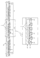
도 3a 내지 도 3k는 본 실시예에 따른 전자 소자 모듈의 제조 방법을 설명하기 위한 단면도.
10: 기판
13: 실장용 전극
20: 접속 도체
28: 외부 접속 단자
30: 밀봉부
31: 제1 밀봉부
35: 제2 밀봉부
100: 전자 소자 모듈
Claims (9)
- 기판;
상기 기판의 일면에 실장되는 전자 소자;
상기 전자 소자를 매립하며 상기 기판의 일면에 형성되는 밀봉부; 및
상기 밀봉부를 관통하며 일단이 상기 기판에 연결되는 접속 도체;
를 포함하는 전자 소자 모듈.
- 제1항에 있어서,
상기 접속 도체의 타단에 접합되며, 상기 밀봉부의 외부에 배치되는 외부 접속 단자를 더 포함하는 전자 소자 모듈.
- 제1항에 있어서,
상기 기판의 타면에 실장되는 전자 소자와, 상기 기판의 타면에 형성되는 밀봉부를 더 포함하는 전자 소자 모듈.
- 기판을 준비하는 단계;
상기 기판의 일면에 전자 소자들을 실장하는 단계;
상기 기판의 일면에 접속 도체를 형성하는 단계; 및
상기 전자 소자들과 상기 접속 도체를 매립하는 밀봉부를 형성하는 단계;
를 포함하는 전자 소자 모듈 제조 방법.
- 제4항에 있어서, 상기 접속 도체를 형성하는 단계는,
상기 기판의 하면에 마스크층을 형성하는 단계;
상기 마스크층에 관통 구멍을 형성하는 단계;
상기 관통 구멍 내에 상기 접속 도체를 형성하는 단계; 및
상기 마스크층을 제거하는 단계;
를 포함하는 전자 소자 모듈 제조 방법.
- 제5항에 있어서, 상기 밀봉부를 형성하는 단계 이후,
상기 접속 도체의 하단에 외부 접속 단자를 형성하는 단계를 더 포함하는 전자 소자 모듈 제조 방법.
- 제5항에 있어서, 상기 관통 구멍 내에 상기 접속 도체를 형성하는 단계는,
상기 기판에 형성된 도금선을 이용하여 도금 방식으로 상기 관통 구멍을 채우며 상기 접속 도체를 형성하는 단계인 전자 소자 모듈 제조 방법.
- 제5항에 있어서, 상기 관통 구멍 내에 상기 접속 도체를 형성하는 단계는,
상기 관통 구멍 내에 도전성 페이스트를 채운 후, 상기 도전성 페이스트를 경화시켜 상기 접속 도체를 형성하는 단계인 전자 소자 모듈 제조 방법.
- 제4항에 있어서,
상기 기판의 타면에 전자 소자들을 실장하는 단계;
상기 기판의 타면에 실장된 상기 전자 소자들을 매립하는 밀봉부를 형성하는 단계를 더 포함하는 전자 소자 모듈 제조 방법.
Priority Applications (1)
| Application Number | Priority Date | Filing Date | Title |
|---|---|---|---|
| KR1020160054584A KR20170124769A (ko) | 2016-05-03 | 2016-05-03 | 전자 소자 모듈 및 그 제조 방법 |
Applications Claiming Priority (1)
| Application Number | Priority Date | Filing Date | Title |
|---|---|---|---|
| KR1020160054584A KR20170124769A (ko) | 2016-05-03 | 2016-05-03 | 전자 소자 모듈 및 그 제조 방법 |
Publications (1)
| Publication Number | Publication Date |
|---|---|
| KR20170124769A true KR20170124769A (ko) | 2017-11-13 |
Family
ID=60386165
Family Applications (1)
| Application Number | Title | Priority Date | Filing Date |
|---|---|---|---|
| KR1020160054584A Ceased KR20170124769A (ko) | 2016-05-03 | 2016-05-03 | 전자 소자 모듈 및 그 제조 방법 |
Country Status (1)
| Country | Link |
|---|---|
| KR (1) | KR20170124769A (ko) |
Cited By (4)
| Publication number | Priority date | Publication date | Assignee | Title |
|---|---|---|---|---|
| KR20200090718A (ko) * | 2018-07-24 | 2020-07-29 | 삼성전기주식회사 | 전자 소자 모듈 |
| CN113921404A (zh) * | 2021-09-24 | 2022-01-11 | 青岛歌尔微电子研究院有限公司 | 一种系统级封装结构的封装方法 |
| US11252812B2 (en) | 2018-07-24 | 2022-02-15 | Samsung Electro-Mechanics Co., Ltd. | Electronic device module |
| CN116190325A (zh) * | 2023-02-13 | 2023-05-30 | 环旭(深圳)电子科创有限公司 | 电子封装模块及其制造方法 |
-
2016
- 2016-05-03 KR KR1020160054584A patent/KR20170124769A/ko not_active Ceased
Cited By (4)
| Publication number | Priority date | Publication date | Assignee | Title |
|---|---|---|---|---|
| KR20200090718A (ko) * | 2018-07-24 | 2020-07-29 | 삼성전기주식회사 | 전자 소자 모듈 |
| US11252812B2 (en) | 2018-07-24 | 2022-02-15 | Samsung Electro-Mechanics Co., Ltd. | Electronic device module |
| CN113921404A (zh) * | 2021-09-24 | 2022-01-11 | 青岛歌尔微电子研究院有限公司 | 一种系统级封装结构的封装方法 |
| CN116190325A (zh) * | 2023-02-13 | 2023-05-30 | 环旭(深圳)电子科创有限公司 | 电子封装模块及其制造方法 |
Similar Documents
| Publication | Publication Date | Title |
|---|---|---|
| US6020629A (en) | Stacked semiconductor package and method of fabrication | |
| KR101994715B1 (ko) | 전자 소자 모듈 제조 방법 | |
| US20150062854A1 (en) | Electronic component module and method of manufacturing the same | |
| KR20150053579A (ko) | 전자 소자 모듈 및 그 제조 방법 | |
| KR20160066311A (ko) | 반도체 패키지 및 반도체 패키지의 제조방법 | |
| TWI907467B (zh) | 具有堆疊被動組件的多層半導體封裝及其形成方法 | |
| US9585260B2 (en) | Electronic component module and manufacturing method thereof | |
| KR101477392B1 (ko) | 전자 소자 모듈 | |
| KR100611291B1 (ko) | 회로 장치, 회로 모듈 및 회로 장치의 제조 방법 | |
| KR20180101832A (ko) | 전자 소자 모듈 및 그 제조 방법 | |
| KR20170124769A (ko) | 전자 소자 모듈 및 그 제조 방법 | |
| US10667419B2 (en) | Manufacturing method of an electronic component module | |
| TWI663663B (zh) | 電子封裝構件及其製作方法 | |
| US9929116B2 (en) | Electronic device module and method of manufacturing the same | |
| US10219380B2 (en) | Electronic device module and manufacturing method thereof | |
| KR20160010246A (ko) | 전자 소자 모듈 및 그 제조 방법 | |
| KR101548801B1 (ko) | 전자 소자 모듈 및 그 제조 방법 | |
| US10356911B2 (en) | Electronic device module and method of manufacturing the same | |
| KR20170008048A (ko) | 전자 소자 모듈 및 그 제조 방법 | |
| KR101681400B1 (ko) | 전자 소자 모듈 및 그 제조 방법 | |
| KR20110080491A (ko) | 반도체 칩 패키지 제조방법 | |
| KR20150000174A (ko) | 전자 소자 모듈 및 그 제조 방법 | |
| KR101922873B1 (ko) | 전자 소자 모듈 제조 방법 | |
| KR101983175B1 (ko) | 전자 소자 모듈 및 그 제조 방법 | |
| KR20160059755A (ko) | 전자 소자 모듈 및 그 제조 방법 |
Legal Events
| Date | Code | Title | Description |
|---|---|---|---|
| PA0109 | Patent application |
St.27 status event code: A-0-1-A10-A12-nap-PA0109 |
|
| PG1501 | Laying open of application |
St.27 status event code: A-1-1-Q10-Q12-nap-PG1501 |
|
| R18-X000 | Changes to party contact information recorded |
St.27 status event code: A-3-3-R10-R18-oth-X000 |
|
| A201 | Request for examination | ||
| PA0201 | Request for examination |
St.27 status event code: A-1-2-D10-D11-exm-PA0201 |
|
| R17-X000 | Change to representative recorded |
St.27 status event code: A-3-3-R10-R17-oth-X000 |
|
| D13-X000 | Search requested |
St.27 status event code: A-1-2-D10-D13-srh-X000 |
|
| D14-X000 | Search report completed |
St.27 status event code: A-1-2-D10-D14-srh-X000 |
|
| E902 | Notification of reason for refusal | ||
| PE0902 | Notice of grounds for rejection |
St.27 status event code: A-1-2-D10-D21-exm-PE0902 |
|
| E601 | Decision to refuse application | ||
| PE0601 | Decision on rejection of patent |
St.27 status event code: N-2-6-B10-B15-exm-PE0601 |
|
| P22-X000 | Classification modified |
St.27 status event code: A-2-2-P10-P22-nap-X000 |
|
| P22-X000 | Classification modified |
St.27 status event code: A-2-2-P10-P22-nap-X000 |