KR20170127202A - 기판지지홀더 및 이를 사용한 기판처리장치 - Google Patents
기판지지홀더 및 이를 사용한 기판처리장치 Download PDFInfo
- Publication number
- KR20170127202A KR20170127202A KR1020160057525A KR20160057525A KR20170127202A KR 20170127202 A KR20170127202 A KR 20170127202A KR 1020160057525 A KR1020160057525 A KR 1020160057525A KR 20160057525 A KR20160057525 A KR 20160057525A KR 20170127202 A KR20170127202 A KR 20170127202A
- Authority
- KR
- South Korea
- Prior art keywords
- substrate
- susceptor
- wire
- frame
- robot
- Prior art date
- Legal status (The legal status is an assumption and is not a legal conclusion. Google has not performed a legal analysis and makes no representation as to the accuracy of the status listed.)
- Ceased
Links
Images



Classifications
-
- H—ELECTRICITY
- H10—SEMICONDUCTOR DEVICES; ELECTRIC SOLID-STATE DEVICES NOT OTHERWISE PROVIDED FOR
- H10P—GENERIC PROCESSES OR APPARATUS FOR THE MANUFACTURE OR TREATMENT OF DEVICES COVERED BY CLASS H10
- H10P72/00—Handling or holding of wafers, substrates or devices during manufacture or treatment thereof
- H10P72/70—Handling or holding of wafers, substrates or devices during manufacture or treatment thereof for supporting or gripping
- H10P72/76—Handling or holding of wafers, substrates or devices during manufacture or treatment thereof for supporting or gripping using mechanical means, e.g. clamps or pinches
- H10P72/7604—Handling or holding of wafers, substrates or devices during manufacture or treatment thereof for supporting or gripping using mechanical means, e.g. clamps or pinches the wafers being placed on a susceptor, stage or support
- H10P72/7611—Handling or holding of wafers, substrates or devices during manufacture or treatment thereof for supporting or gripping using mechanical means, e.g. clamps or pinches the wafers being placed on a susceptor, stage or support characterised by edge profile or support profile
-
- H01L21/68735—
-
- H01L21/67766—
-
- H01L21/6835—
-
- H01L21/68742—
-
- H01L21/68778—
-
- H01L21/68785—
-
- H—ELECTRICITY
- H10—SEMICONDUCTOR DEVICES; ELECTRIC SOLID-STATE DEVICES NOT OTHERWISE PROVIDED FOR
- H10P—GENERIC PROCESSES OR APPARATUS FOR THE MANUFACTURE OR TREATMENT OF DEVICES COVERED BY CLASS H10
- H10P72/00—Handling or holding of wafers, substrates or devices during manufacture or treatment thereof
- H10P72/30—Handling or holding of wafers, substrates or devices during manufacture or treatment thereof for conveying, e.g. between different workstations
-
- H—ELECTRICITY
- H10—SEMICONDUCTOR DEVICES; ELECTRIC SOLID-STATE DEVICES NOT OTHERWISE PROVIDED FOR
- H10P—GENERIC PROCESSES OR APPARATUS FOR THE MANUFACTURE OR TREATMENT OF DEVICES COVERED BY CLASS H10
- H10P72/00—Handling or holding of wafers, substrates or devices during manufacture or treatment thereof
- H10P72/30—Handling or holding of wafers, substrates or devices during manufacture or treatment thereof for conveying, e.g. between different workstations
- H10P72/34—Handling or holding of wafers, substrates or devices during manufacture or treatment thereof for conveying, e.g. between different workstations the wafers being stored in a carrier, involving loading and unloading
- H10P72/3402—Mechanical parts of transfer devices
-
- H—ELECTRICITY
- H10—SEMICONDUCTOR DEVICES; ELECTRIC SOLID-STATE DEVICES NOT OTHERWISE PROVIDED FOR
- H10P—GENERIC PROCESSES OR APPARATUS FOR THE MANUFACTURE OR TREATMENT OF DEVICES COVERED BY CLASS H10
- H10P72/00—Handling or holding of wafers, substrates or devices during manufacture or treatment thereof
- H10P72/70—Handling or holding of wafers, substrates or devices during manufacture or treatment thereof for supporting or gripping
-
- H—ELECTRICITY
- H10—SEMICONDUCTOR DEVICES; ELECTRIC SOLID-STATE DEVICES NOT OTHERWISE PROVIDED FOR
- H10P—GENERIC PROCESSES OR APPARATUS FOR THE MANUFACTURE OR TREATMENT OF DEVICES COVERED BY CLASS H10
- H10P72/00—Handling or holding of wafers, substrates or devices during manufacture or treatment thereof
- H10P72/70—Handling or holding of wafers, substrates or devices during manufacture or treatment thereof for supporting or gripping
- H10P72/74—Handling or holding of wafers, substrates or devices during manufacture or treatment thereof for supporting or gripping using temporarily an auxiliary support
-
- H—ELECTRICITY
- H10—SEMICONDUCTOR DEVICES; ELECTRIC SOLID-STATE DEVICES NOT OTHERWISE PROVIDED FOR
- H10P—GENERIC PROCESSES OR APPARATUS FOR THE MANUFACTURE OR TREATMENT OF DEVICES COVERED BY CLASS H10
- H10P72/00—Handling or holding of wafers, substrates or devices during manufacture or treatment thereof
- H10P72/70—Handling or holding of wafers, substrates or devices during manufacture or treatment thereof for supporting or gripping
- H10P72/76—Handling or holding of wafers, substrates or devices during manufacture or treatment thereof for supporting or gripping using mechanical means, e.g. clamps or pinches
-
- H—ELECTRICITY
- H10—SEMICONDUCTOR DEVICES; ELECTRIC SOLID-STATE DEVICES NOT OTHERWISE PROVIDED FOR
- H10P—GENERIC PROCESSES OR APPARATUS FOR THE MANUFACTURE OR TREATMENT OF DEVICES COVERED BY CLASS H10
- H10P72/00—Handling or holding of wafers, substrates or devices during manufacture or treatment thereof
- H10P72/70—Handling or holding of wafers, substrates or devices during manufacture or treatment thereof for supporting or gripping
- H10P72/76—Handling or holding of wafers, substrates or devices during manufacture or treatment thereof for supporting or gripping using mechanical means, e.g. clamps or pinches
- H10P72/7604—Handling or holding of wafers, substrates or devices during manufacture or treatment thereof for supporting or gripping using mechanical means, e.g. clamps or pinches the wafers being placed on a susceptor, stage or support
- H10P72/7612—Handling or holding of wafers, substrates or devices during manufacture or treatment thereof for supporting or gripping using mechanical means, e.g. clamps or pinches the wafers being placed on a susceptor, stage or support characterised by lifting arrangements, e.g. lift pins
-
- H—ELECTRICITY
- H10—SEMICONDUCTOR DEVICES; ELECTRIC SOLID-STATE DEVICES NOT OTHERWISE PROVIDED FOR
- H10P—GENERIC PROCESSES OR APPARATUS FOR THE MANUFACTURE OR TREATMENT OF DEVICES COVERED BY CLASS H10
- H10P72/00—Handling or holding of wafers, substrates or devices during manufacture or treatment thereof
- H10P72/70—Handling or holding of wafers, substrates or devices during manufacture or treatment thereof for supporting or gripping
- H10P72/76—Handling or holding of wafers, substrates or devices during manufacture or treatment thereof for supporting or gripping using mechanical means, e.g. clamps or pinches
- H10P72/7604—Handling or holding of wafers, substrates or devices during manufacture or treatment thereof for supporting or gripping using mechanical means, e.g. clamps or pinches the wafers being placed on a susceptor, stage or support
- H10P72/7622—Handling or holding of wafers, substrates or devices during manufacture or treatment thereof for supporting or gripping using mechanical means, e.g. clamps or pinches the wafers being placed on a susceptor, stage or support characterised by supporting substrates others than wafers, e.g. chips
-
- H—ELECTRICITY
- H10—SEMICONDUCTOR DEVICES; ELECTRIC SOLID-STATE DEVICES NOT OTHERWISE PROVIDED FOR
- H10P—GENERIC PROCESSES OR APPARATUS FOR THE MANUFACTURE OR TREATMENT OF DEVICES COVERED BY CLASS H10
- H10P72/00—Handling or holding of wafers, substrates or devices during manufacture or treatment thereof
- H10P72/70—Handling or holding of wafers, substrates or devices during manufacture or treatment thereof for supporting or gripping
- H10P72/76—Handling or holding of wafers, substrates or devices during manufacture or treatment thereof for supporting or gripping using mechanical means, e.g. clamps or pinches
- H10P72/7604—Handling or holding of wafers, substrates or devices during manufacture or treatment thereof for supporting or gripping using mechanical means, e.g. clamps or pinches the wafers being placed on a susceptor, stage or support
- H10P72/7624—Handling or holding of wafers, substrates or devices during manufacture or treatment thereof for supporting or gripping using mechanical means, e.g. clamps or pinches the wafers being placed on a susceptor, stage or support characterised by the mechanical construction of the susceptor, stage or support
Landscapes
- Container, Conveyance, Adherence, Positioning, Of Wafer (AREA)
- Chemical Vapour Deposition (AREA)
- Engineering & Computer Science (AREA)
- Robotics (AREA)
Abstract
Description
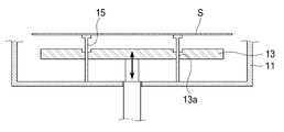
도 2는 본 발명의 일 실시예에 따른 기판처리장치의 정단면도.
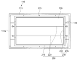
도 3은 본 발명의 일 실시예에 따른 기판처리장치의 평단면도.
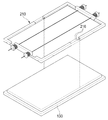
도 4는 도 3에 도시된 기판지지홀더 및 서셉터의 사시도.
도 5a 내지 5d는 본 발명의 일 실시예에 따른 기판처리장치에 기판을 반입하는 것을 보인 도.
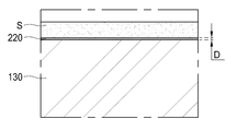
도 6은 도 5d의 "A"부 확대도.
도 7은 본 발명의 다른 실시예에 따른 기판지지홀더 및 서셉터의 사시도.
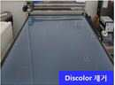
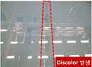
| 와이어의 직경 = 0.3㎜ | 와이어의 직경 = 1.0㎜ |
 |
 |
| 와이어의 직경 = 3.0㎜ | 와이어의 직경 = 4.0㎜ |
 |
 |
130: 서셉터
200: 기핀지지홀더
210: 프레임
220: 와이어
Claims (13)
- 일면이 개방되어 기판이 탑재된 로봇의 아암이 출입하는 프레임;
상기 프레임의 개방된 일면측 및 개방된 일면과 대향하는 대향면측에 일단부 및 타단부가 각각 지지되어 기판을 지지하는 복수의 와이어(Wire)를 포함하며,
상기 와이어의 직경은 0.1㎜∼3㎜인 것을 특징으로 하는 기판지지홀더. - 제1항에 있어서,
상기 와이어는 알루미늄, 스테인리스 스틸 및 티타늄 중에서 선택된 어느 하나인 것을 특징으로 하는 기판지지홀더. - 제1항에 있어서,
상기 프레임의 개방된 일면측 및 상기 프레임의 개방된 일면과 대향하는 대향면에는 상기 와이어의 일단부측 및 타단부측을 각각 지지함과 동시에 상기 와이어의 장력을 조절하기 위한 장력조절모듈이 상호 대향되게 설치된 것을 특징으로 하는 기판지지홀더. - 제3항에 있어서,
상기 프레임의 개방된 일면에는 상기 프레임의 개방된 일면 일측 및 타측을 연결함과 동시에 상기 장력조절모듈이 설치되는 브라켓이 설치된 것을 특징으로 하는 기판지지홀더. - 제4항에 있어서,
상기 와이어의 양단부측에는 나선(螺線)이 형성되고,
상기 장력조절모듈은,
상기 브라켓 및 상기 프레임의 개방된 일면과 대향하는 대향면에 각각 설치되며, 상기 와이어의 단부측이 관통하면서 지지되는 지지블럭;
상기 지지블럭을 관통한 상기 와이어의 단부측에 각각 회전가능하게 결합되며 회전함에 따라 상기 지지블럭을 기준으로 상기 와이어를 신축(伸縮)시키는 조절너트를 포함하는 것을 특징으로 하는 기판지지홀더. - 제3항에 있어서,
상기 프레임의 상면과 상기 와이어의 최상측 외주면은 상기 프레임의 하면을 기준으로 동일 높이에 위치된 것을 특징으로 하는 기판지지홀더. - 기판이 반입되어 처리되는 공간을 제공하는 챔버;
상기 챔버의 내부에 승강가능하게 설치되며, 상승하여 기판을 탑재 지지하는 서셉터;
상기 서셉터의 상측 상기 챔버의 내부에 설치되며, 상기 서셉터가 승강함에 따라, 로봇의 아암에 탑재된 기판을 전달받아 상기 서셉터의 상면에 탑재시키거나, 상기 서셉터의 상면에 탑재된 기판을 상기 서셉터로부터 이격시키는, 청구항1 내지 청구항6 중, 어느 한 항에 따른 기판지지홀더를 포함하는 것을 특징으로 하는 기판처리장치. - 제7항에 있어서,
상기 기판지지홀더는 상기 서셉터에 의하여 승강하는 것을 특징으로 하는 기판지지홀더. - 제8항에 있어서,
상기 서셉터는 상측 부위가 하측 부위 보다 작은 크기로 형성되고,
상기 서셉터가 상승하면, 상기 서셉터의 하측 부위 테두리부는 상기 프레임의 하면과 접촉하고 상기 서셉터의 상측 부위는 상기 프레임의 내부에 위치되어 상기 와이어 및 상기 와이어에 지지된 기판과 접촉하는 것을 특징으로 하는 기판처리장치. - 제8항에 있어서,
상기 서셉터는 상측 부위가 하측 부위 보다 작은 크기로 형성되고,
상기 프레임의 내주면측 하면에는 수직면과 수평면을 가지는 단면(段面)이 형성되며,
상기 서셉터가 상승하면, 상기 서셉터의 하측 부위 테두리부는 상기 단면의 상기 수평면과 접촉하고 상기 서셉터의 상측 부위는 상기 프레임의 내부에 위치되어 상기 와이어 및 상기 와이어에 지지된 기판과 접촉하는 것을 특징으로 하는 기판처리장치. - 제8항에 있어서,
상기 챔버의 내면에는 상기 프레임의 하면을 지지하는 복수의 지지핀이 설치되고,
상기 프레임의 하면에는 상기 지지핀이 삽입되는 지지홈이 형성된 것을 특징으로 하는 기판처리장치. - 기판이 반입되어 처리되는 공간을 제공하는 챔버;
상기 챔버의 내부에 승강가능하게 설치되며, 상승하여 기판을 탑재 지지하는 서셉터;
상기 서셉터 상측 상기 챔버의 내부에 설치되고 일면이 개방되어 기판이 탑재된 로봇의 아암이 출입하는 프레임, 상기 프레임의 개방된 일면측 및 개방된 일면과 대향하는 대향면측에 일단부 및 타단부가 각각 지지되며 상기 서셉터가 승강함에 따라 로봇의 아암에 탑재된 기판을 전달받아 상기 서셉터의 상면에 탑재시키거나 상기 서셉터의 상면에 탑재된 기판을 상기 서셉터로부터 이격시키는 복수의 와이어(Wire)를 가지는 기판지지홀더를 포함하며,
기판의 처리시 상기 서셉터와 기판은 0.1㎜∼3㎜의 간격을 가지는 것을 특징으로 하는 기판처리장치. - 제12항에 있어서,
상기 와이어는 상기 서셉터와 기판 사이에 게재되고,
기판과 상기 서셉터 사이의 간격과 상기 와이어의 직경은 대응되는 것을 특징으로 하는 기판처리장치.
Priority Applications (3)
| Application Number | Priority Date | Filing Date | Title |
|---|---|---|---|
| KR1020160057525A KR20170127202A (ko) | 2016-05-11 | 2016-05-11 | 기판지지홀더 및 이를 사용한 기판처리장치 |
| PCT/KR2016/007562 WO2017195933A1 (ko) | 2016-05-11 | 2016-07-12 | 기판지지홀더 및 이를 사용한 기판처리장치 |
| TW105124692A TW201740499A (zh) | 2016-05-11 | 2016-08-03 | 基板支架以及使用該基板支架之基板處理設備 |
Applications Claiming Priority (1)
| Application Number | Priority Date | Filing Date | Title |
|---|---|---|---|
| KR1020160057525A KR20170127202A (ko) | 2016-05-11 | 2016-05-11 | 기판지지홀더 및 이를 사용한 기판처리장치 |
Publications (1)
| Publication Number | Publication Date |
|---|---|
| KR20170127202A true KR20170127202A (ko) | 2017-11-21 |
Family
ID=60267866
Family Applications (1)
| Application Number | Title | Priority Date | Filing Date |
|---|---|---|---|
| KR1020160057525A Ceased KR20170127202A (ko) | 2016-05-11 | 2016-05-11 | 기판지지홀더 및 이를 사용한 기판처리장치 |
Country Status (3)
| Country | Link |
|---|---|
| KR (1) | KR20170127202A (ko) |
| TW (1) | TW201740499A (ko) |
| WO (1) | WO2017195933A1 (ko) |
Cited By (1)
| Publication number | Priority date | Publication date | Assignee | Title |
|---|---|---|---|---|
| KR20190114383A (ko) | 2018-03-30 | 2019-10-10 | 코오롱인더스트리 주식회사 | 유기발광 다이오드 패널의 봉지층 형성용 필름, 이 필름을 갖는 유기발광 다이오드 패널 및 그 제조방법 |
Family Cites Families (5)
| Publication number | Priority date | Publication date | Assignee | Title |
|---|---|---|---|---|
| JP3457900B2 (ja) * | 1998-11-18 | 2003-10-20 | 東京エレクトロン株式会社 | 基板熱処理装置及び基板熱処理方法 |
| KR101026323B1 (ko) * | 2002-11-27 | 2011-03-31 | 도쿄엘렉트론가부시키가이샤 | 기판처리장치 |
| KR101196197B1 (ko) * | 2004-01-20 | 2012-11-02 | 주성엔지니어링(주) | 기판 지지부재, 이를 포함하는 증착 장치 및 이를 이용한기판의 이송 방법 |
| KR20140028579A (ko) * | 2012-08-29 | 2014-03-10 | 세메스 주식회사 | 기판처리장치 |
| KR101511714B1 (ko) * | 2013-08-29 | 2015-04-13 | 박성우 | 평판 적재용 와이어랙의 와이어 장력 조절장치 |
-
2016
- 2016-05-11 KR KR1020160057525A patent/KR20170127202A/ko not_active Ceased
- 2016-07-12 WO PCT/KR2016/007562 patent/WO2017195933A1/ko not_active Ceased
- 2016-08-03 TW TW105124692A patent/TW201740499A/zh unknown
Cited By (1)
| Publication number | Priority date | Publication date | Assignee | Title |
|---|---|---|---|---|
| KR20190114383A (ko) | 2018-03-30 | 2019-10-10 | 코오롱인더스트리 주식회사 | 유기발광 다이오드 패널의 봉지층 형성용 필름, 이 필름을 갖는 유기발광 다이오드 패널 및 그 제조방법 |
Also Published As
| Publication number | Publication date |
|---|---|
| WO2017195933A1 (ko) | 2017-11-16 |
| TW201740499A (zh) | 2017-11-16 |
Similar Documents
| Publication | Publication Date | Title |
|---|---|---|
| US9698042B1 (en) | Wafer centering in pocket to improve azimuthal thickness uniformity at wafer edge | |
| KR100909499B1 (ko) | 기판의 탑재 기구 및 기판 처리 장치 | |
| JP2918780B2 (ja) | 加熱された支持部上のシャドーフレーム及び大型平面基板の整列 | |
| US8118940B2 (en) | Clamping mechanism for semiconductor device | |
| EP0777264A1 (en) | Semiconductor wafer alignment member and clamp ring | |
| KR102015657B1 (ko) | 진공 처리 장치를 위한 접지 어셈블리 | |
| KR20210004847A (ko) | 기판 처리 장치 및 기판의 전달 방법 | |
| US6609869B2 (en) | Transfer chamber with integral loadlock and staging station | |
| JPH1180950A (ja) | ウェハをアラインメントさせる装置および方法 | |
| CN107154368B (zh) | 准分子激光退火装置用基板支撑模块 | |
| KR20170127202A (ko) | 기판지지홀더 및 이를 사용한 기판처리장치 | |
| KR20190063286A (ko) | 리프트핀유닛의 이동방법 및 기판처리장치 | |
| CN102024732B (zh) | 基片加工装置的基片交换模块及有该模块的基片加工装置 | |
| KR102885118B1 (ko) | 기판처리방법 | |
| US20220356575A1 (en) | Substrate processing apparatus and method | |
| JP2001181845A (ja) | 成膜装置 | |
| KR20170126111A (ko) | 리프트핀용 지지유닛 및 이를 사용한 기판처리장치 | |
| KR102910143B1 (ko) | 기판처리장치 및 기판처리방법 | |
| KR101297670B1 (ko) | 기판 처리 장치 | |
| KR101831312B1 (ko) | 기판처리시스템 및 기판처리방법 | |
| KR101297666B1 (ko) | 기판 처리 장치 | |
| KR102297311B1 (ko) | 기판 지지 어셈블리 및 이를 포함하는 기판 처리 장치 | |
| KR101738844B1 (ko) | 박막증착장치 | |
| KR20050112731A (ko) | 반도체 제조설비의 리프트핀 어셈블리 | |
| KR100783282B1 (ko) | 정열 챔버의 정열대 |
Legal Events
| Date | Code | Title | Description |
|---|---|---|---|
| PA0109 | Patent application |
St.27 status event code: A-0-1-A10-A12-nap-PA0109 |
|
| P11-X000 | Amendment of application requested |
St.27 status event code: A-2-2-P10-P11-nap-X000 |
|
| P13-X000 | Application amended |
St.27 status event code: A-2-2-P10-P13-nap-X000 |
|
| A201 | Request for examination | ||
| PA0201 | Request for examination |
St.27 status event code: A-1-2-D10-D11-exm-PA0201 |
|
| PG1501 | Laying open of application |
St.27 status event code: A-1-1-Q10-Q12-nap-PG1501 |
|
| E902 | Notification of reason for refusal | ||
| PE0902 | Notice of grounds for rejection |
St.27 status event code: A-1-2-D10-D21-exm-PE0902 |
|
| E601 | Decision to refuse application | ||
| PE0601 | Decision on rejection of patent |
St.27 status event code: N-2-6-B10-B15-exm-PE0601 |
|
| R18-X000 | Changes to party contact information recorded |
St.27 status event code: A-3-3-R10-R18-oth-X000 |
|
| R18-X000 | Changes to party contact information recorded |
St.27 status event code: A-3-3-R10-R18-oth-X000 |
|
| P22-X000 | Classification modified |
St.27 status event code: A-2-2-P10-P22-nap-X000 |