KR20170128770A - 명점 복구를 거친 후의 액정 패널 및 그 명점 복구 방법 - Google Patents
명점 복구를 거친 후의 액정 패널 및 그 명점 복구 방법 Download PDFInfo
- Publication number
- KR20170128770A KR20170128770A KR1020177023536A KR20177023536A KR20170128770A KR 20170128770 A KR20170128770 A KR 20170128770A KR 1020177023536 A KR1020177023536 A KR 1020177023536A KR 20177023536 A KR20177023536 A KR 20177023536A KR 20170128770 A KR20170128770 A KR 20170128770A
- Authority
- KR
- South Korea
- Prior art keywords
- electrode
- pixel unit
- sub
- film transistor
- thin film
- Prior art date
- Legal status (The legal status is an assumption and is not a legal conclusion. Google has not performed a legal analysis and makes no representation as to the accuracy of the status listed.)
- Granted
Links
Images

Classifications
-
- G—PHYSICS
- G02—OPTICS
- G02F—OPTICAL DEVICES OR ARRANGEMENTS FOR THE CONTROL OF LIGHT BY MODIFICATION OF THE OPTICAL PROPERTIES OF THE MEDIA OF THE ELEMENTS INVOLVED THEREIN; NON-LINEAR OPTICS; FREQUENCY-CHANGING OF LIGHT; OPTICAL LOGIC ELEMENTS; OPTICAL ANALOGUE/DIGITAL CONVERTERS
- G02F1/00—Devices or arrangements for the control of the intensity, colour, phase, polarisation or direction of light arriving from an independent light source, e.g. switching, gating or modulating; Non-linear optics
- G02F1/01—Devices or arrangements for the control of the intensity, colour, phase, polarisation or direction of light arriving from an independent light source, e.g. switching, gating or modulating; Non-linear optics for the control of the intensity, phase, polarisation or colour
- G02F1/13—Devices or arrangements for the control of the intensity, colour, phase, polarisation or direction of light arriving from an independent light source, e.g. switching, gating or modulating; Non-linear optics for the control of the intensity, phase, polarisation or colour based on liquid crystals, e.g. single liquid crystal display cells
- G02F1/133—Constructional arrangements; Operation of liquid crystal cells; Circuit arrangements
- G02F1/1333—Constructional arrangements; Manufacturing methods
- G02F1/1343—Electrodes
-
- G—PHYSICS
- G02—OPTICS
- G02F—OPTICAL DEVICES OR ARRANGEMENTS FOR THE CONTROL OF LIGHT BY MODIFICATION OF THE OPTICAL PROPERTIES OF THE MEDIA OF THE ELEMENTS INVOLVED THEREIN; NON-LINEAR OPTICS; FREQUENCY-CHANGING OF LIGHT; OPTICAL LOGIC ELEMENTS; OPTICAL ANALOGUE/DIGITAL CONVERTERS
- G02F1/00—Devices or arrangements for the control of the intensity, colour, phase, polarisation or direction of light arriving from an independent light source, e.g. switching, gating or modulating; Non-linear optics
- G02F1/01—Devices or arrangements for the control of the intensity, colour, phase, polarisation or direction of light arriving from an independent light source, e.g. switching, gating or modulating; Non-linear optics for the control of the intensity, phase, polarisation or colour
- G02F1/13—Devices or arrangements for the control of the intensity, colour, phase, polarisation or direction of light arriving from an independent light source, e.g. switching, gating or modulating; Non-linear optics for the control of the intensity, phase, polarisation or colour based on liquid crystals, e.g. single liquid crystal display cells
- G02F1/133—Constructional arrangements; Operation of liquid crystal cells; Circuit arrangements
- G02F1/136—Liquid crystal cells structurally associated with a semi-conducting layer or substrate, e.g. cells forming part of an integrated circuit
- G02F1/1362—Active matrix addressed cells
- G02F1/136259—Repairing; Defects
-
- G—PHYSICS
- G02—OPTICS
- G02F—OPTICAL DEVICES OR ARRANGEMENTS FOR THE CONTROL OF LIGHT BY MODIFICATION OF THE OPTICAL PROPERTIES OF THE MEDIA OF THE ELEMENTS INVOLVED THEREIN; NON-LINEAR OPTICS; FREQUENCY-CHANGING OF LIGHT; OPTICAL LOGIC ELEMENTS; OPTICAL ANALOGUE/DIGITAL CONVERTERS
- G02F1/00—Devices or arrangements for the control of the intensity, colour, phase, polarisation or direction of light arriving from an independent light source, e.g. switching, gating or modulating; Non-linear optics
- G02F1/01—Devices or arrangements for the control of the intensity, colour, phase, polarisation or direction of light arriving from an independent light source, e.g. switching, gating or modulating; Non-linear optics for the control of the intensity, phase, polarisation or colour
- G02F1/13—Devices or arrangements for the control of the intensity, colour, phase, polarisation or direction of light arriving from an independent light source, e.g. switching, gating or modulating; Non-linear optics for the control of the intensity, phase, polarisation or colour based on liquid crystals, e.g. single liquid crystal display cells
-
- G—PHYSICS
- G02—OPTICS
- G02F—OPTICAL DEVICES OR ARRANGEMENTS FOR THE CONTROL OF LIGHT BY MODIFICATION OF THE OPTICAL PROPERTIES OF THE MEDIA OF THE ELEMENTS INVOLVED THEREIN; NON-LINEAR OPTICS; FREQUENCY-CHANGING OF LIGHT; OPTICAL LOGIC ELEMENTS; OPTICAL ANALOGUE/DIGITAL CONVERTERS
- G02F1/00—Devices or arrangements for the control of the intensity, colour, phase, polarisation or direction of light arriving from an independent light source, e.g. switching, gating or modulating; Non-linear optics
- G02F1/01—Devices or arrangements for the control of the intensity, colour, phase, polarisation or direction of light arriving from an independent light source, e.g. switching, gating or modulating; Non-linear optics for the control of the intensity, phase, polarisation or colour
- G02F1/13—Devices or arrangements for the control of the intensity, colour, phase, polarisation or direction of light arriving from an independent light source, e.g. switching, gating or modulating; Non-linear optics for the control of the intensity, phase, polarisation or colour based on liquid crystals, e.g. single liquid crystal display cells
- G02F1/1306—Details
- G02F1/1309—Repairing; Testing
-
- G—PHYSICS
- G02—OPTICS
- G02F—OPTICAL DEVICES OR ARRANGEMENTS FOR THE CONTROL OF LIGHT BY MODIFICATION OF THE OPTICAL PROPERTIES OF THE MEDIA OF THE ELEMENTS INVOLVED THEREIN; NON-LINEAR OPTICS; FREQUENCY-CHANGING OF LIGHT; OPTICAL LOGIC ELEMENTS; OPTICAL ANALOGUE/DIGITAL CONVERTERS
- G02F1/00—Devices or arrangements for the control of the intensity, colour, phase, polarisation or direction of light arriving from an independent light source, e.g. switching, gating or modulating; Non-linear optics
- G02F1/01—Devices or arrangements for the control of the intensity, colour, phase, polarisation or direction of light arriving from an independent light source, e.g. switching, gating or modulating; Non-linear optics for the control of the intensity, phase, polarisation or colour
- G02F1/13—Devices or arrangements for the control of the intensity, colour, phase, polarisation or direction of light arriving from an independent light source, e.g. switching, gating or modulating; Non-linear optics for the control of the intensity, phase, polarisation or colour based on liquid crystals, e.g. single liquid crystal display cells
- G02F1/133—Constructional arrangements; Operation of liquid crystal cells; Circuit arrangements
- G02F1/136—Liquid crystal cells structurally associated with a semi-conducting layer or substrate, e.g. cells forming part of an integrated circuit
- G02F1/1362—Active matrix addressed cells
- G02F1/13624—Active matrix addressed cells having more than one switching element per pixel
-
- G—PHYSICS
- G02—OPTICS
- G02F—OPTICAL DEVICES OR ARRANGEMENTS FOR THE CONTROL OF LIGHT BY MODIFICATION OF THE OPTICAL PROPERTIES OF THE MEDIA OF THE ELEMENTS INVOLVED THEREIN; NON-LINEAR OPTICS; FREQUENCY-CHANGING OF LIGHT; OPTICAL LOGIC ELEMENTS; OPTICAL ANALOGUE/DIGITAL CONVERTERS
- G02F1/00—Devices or arrangements for the control of the intensity, colour, phase, polarisation or direction of light arriving from an independent light source, e.g. switching, gating or modulating; Non-linear optics
- G02F1/01—Devices or arrangements for the control of the intensity, colour, phase, polarisation or direction of light arriving from an independent light source, e.g. switching, gating or modulating; Non-linear optics for the control of the intensity, phase, polarisation or colour
- G02F1/13—Devices or arrangements for the control of the intensity, colour, phase, polarisation or direction of light arriving from an independent light source, e.g. switching, gating or modulating; Non-linear optics for the control of the intensity, phase, polarisation or colour based on liquid crystals, e.g. single liquid crystal display cells
- G02F1/133—Constructional arrangements; Operation of liquid crystal cells; Circuit arrangements
- G02F1/136—Liquid crystal cells structurally associated with a semi-conducting layer or substrate, e.g. cells forming part of an integrated circuit
- G02F1/1362—Active matrix addressed cells
- G02F1/136259—Repairing; Defects
- G02F1/136263—Line defects
-
- G—PHYSICS
- G02—OPTICS
- G02F—OPTICAL DEVICES OR ARRANGEMENTS FOR THE CONTROL OF LIGHT BY MODIFICATION OF THE OPTICAL PROPERTIES OF THE MEDIA OF THE ELEMENTS INVOLVED THEREIN; NON-LINEAR OPTICS; FREQUENCY-CHANGING OF LIGHT; OPTICAL LOGIC ELEMENTS; OPTICAL ANALOGUE/DIGITAL CONVERTERS
- G02F1/00—Devices or arrangements for the control of the intensity, colour, phase, polarisation or direction of light arriving from an independent light source, e.g. switching, gating or modulating; Non-linear optics
- G02F1/01—Devices or arrangements for the control of the intensity, colour, phase, polarisation or direction of light arriving from an independent light source, e.g. switching, gating or modulating; Non-linear optics for the control of the intensity, phase, polarisation or colour
- G02F1/13—Devices or arrangements for the control of the intensity, colour, phase, polarisation or direction of light arriving from an independent light source, e.g. switching, gating or modulating; Non-linear optics for the control of the intensity, phase, polarisation or colour based on liquid crystals, e.g. single liquid crystal display cells
- G02F1/133—Constructional arrangements; Operation of liquid crystal cells; Circuit arrangements
- G02F1/136—Liquid crystal cells structurally associated with a semi-conducting layer or substrate, e.g. cells forming part of an integrated circuit
- G02F1/1362—Active matrix addressed cells
- G02F1/136286—Wiring, e.g. gate line, drain line
-
- G—PHYSICS
- G02—OPTICS
- G02F—OPTICAL DEVICES OR ARRANGEMENTS FOR THE CONTROL OF LIGHT BY MODIFICATION OF THE OPTICAL PROPERTIES OF THE MEDIA OF THE ELEMENTS INVOLVED THEREIN; NON-LINEAR OPTICS; FREQUENCY-CHANGING OF LIGHT; OPTICAL LOGIC ELEMENTS; OPTICAL ANALOGUE/DIGITAL CONVERTERS
- G02F1/00—Devices or arrangements for the control of the intensity, colour, phase, polarisation or direction of light arriving from an independent light source, e.g. switching, gating or modulating; Non-linear optics
- G02F1/01—Devices or arrangements for the control of the intensity, colour, phase, polarisation or direction of light arriving from an independent light source, e.g. switching, gating or modulating; Non-linear optics for the control of the intensity, phase, polarisation or colour
- G02F1/13—Devices or arrangements for the control of the intensity, colour, phase, polarisation or direction of light arriving from an independent light source, e.g. switching, gating or modulating; Non-linear optics for the control of the intensity, phase, polarisation or colour based on liquid crystals, e.g. single liquid crystal display cells
- G02F1/133—Constructional arrangements; Operation of liquid crystal cells; Circuit arrangements
- G02F1/136—Liquid crystal cells structurally associated with a semi-conducting layer or substrate, e.g. cells forming part of an integrated circuit
- G02F1/1362—Active matrix addressed cells
- G02F1/1368—Active matrix addressed cells in which the switching element is a three-electrode device
-
- H01L27/124—
-
- H—ELECTRICITY
- H10—SEMICONDUCTOR DEVICES; ELECTRIC SOLID-STATE DEVICES NOT OTHERWISE PROVIDED FOR
- H10D—INORGANIC ELECTRIC SEMICONDUCTOR DEVICES
- H10D86/00—Integrated devices formed in or on insulating or conducting substrates, e.g. formed in silicon-on-insulator [SOI] substrates or on stainless steel or glass substrates
- H10D86/40—Integrated devices formed in or on insulating or conducting substrates, e.g. formed in silicon-on-insulator [SOI] substrates or on stainless steel or glass substrates characterised by multiple TFTs
- H10D86/441—Interconnections, e.g. scanning lines
-
- H—ELECTRICITY
- H10—SEMICONDUCTOR DEVICES; ELECTRIC SOLID-STATE DEVICES NOT OTHERWISE PROVIDED FOR
- H10D—INORGANIC ELECTRIC SEMICONDUCTOR DEVICES
- H10D86/00—Integrated devices formed in or on insulating or conducting substrates, e.g. formed in silicon-on-insulator [SOI] substrates or on stainless steel or glass substrates
- H10D86/40—Integrated devices formed in or on insulating or conducting substrates, e.g. formed in silicon-on-insulator [SOI] substrates or on stainless steel or glass substrates characterised by multiple TFTs
- H10D86/481—Integrated devices formed in or on insulating or conducting substrates, e.g. formed in silicon-on-insulator [SOI] substrates or on stainless steel or glass substrates characterised by multiple TFTs integrated with passive devices, e.g. auxiliary capacitors
-
- H—ELECTRICITY
- H10—SEMICONDUCTOR DEVICES; ELECTRIC SOLID-STATE DEVICES NOT OTHERWISE PROVIDED FOR
- H10D—INORGANIC ELECTRIC SEMICONDUCTOR DEVICES
- H10D86/00—Integrated devices formed in or on insulating or conducting substrates, e.g. formed in silicon-on-insulator [SOI] substrates or on stainless steel or glass substrates
- H10D86/40—Integrated devices formed in or on insulating or conducting substrates, e.g. formed in silicon-on-insulator [SOI] substrates or on stainless steel or glass substrates characterised by multiple TFTs
- H10D86/60—Integrated devices formed in or on insulating or conducting substrates, e.g. formed in silicon-on-insulator [SOI] substrates or on stainless steel or glass substrates characterised by multiple TFTs wherein the TFTs are in active matrices
-
- G02F2001/136263—
-
- G—PHYSICS
- G02—OPTICS
- G02F—OPTICAL DEVICES OR ARRANGEMENTS FOR THE CONTROL OF LIGHT BY MODIFICATION OF THE OPTICAL PROPERTIES OF THE MEDIA OF THE ELEMENTS INVOLVED THEREIN; NON-LINEAR OPTICS; FREQUENCY-CHANGING OF LIGHT; OPTICAL LOGIC ELEMENTS; OPTICAL ANALOGUE/DIGITAL CONVERTERS
- G02F2201/00—Constructional arrangements not provided for in groups G02F1/00 - G02F7/00
- G02F2201/50—Protective arrangements
- G02F2201/506—Repairing, e.g. with redundant arrangement against defective part
- G02F2201/508—Pseudo repairing, e.g. a defective part is brought into a condition in which it does not disturb the functioning of the device
Landscapes
- Physics & Mathematics (AREA)
- Nonlinear Science (AREA)
- Chemical & Material Sciences (AREA)
- Crystallography & Structural Chemistry (AREA)
- General Physics & Mathematics (AREA)
- Optics & Photonics (AREA)
- Mathematical Physics (AREA)
- Engineering & Computer Science (AREA)
- Microelectronics & Electronic Packaging (AREA)
- Liquid Crystal (AREA)
Abstract
Description

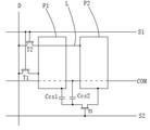
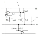
도 2는 도 1에 도시된 바와 같은 전하 공유형 화소 구조의 등가적 회로도이다.
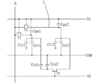
도 3은 종래기술 중에서 서브 화소 유닛에 대해 명점 복구를 수행하는 모식도이다.
도 4는 하나의 화소 유닛이 수신한 전압 신호의 파형도이다.
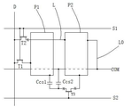
도 5는 본 발명의 실시예에서 서브 화소 유닛에 대해 명점 복구를 수행하는 모식도이다.
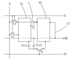
도 6은 본 발명의 실시예 중에서 서브 화소 유닛에 대해 명점 복구를 수행한 후의 등가적 회로도이다.
Claims (10)
- 명점 복구를 거친 후의 액정 패널에 있어서,
상기 액정 패널은 어레이 기판을 포함하고, 상기 어레이 기판은 적어도 한 명점 복구를 거친 후의 화소 구조를 포함하며, 상기 화소 구조는,
한 데이터 라인;
제 1 스캔 라인 및 제 2 스캔 라인;
한 공용 전극 배선;
메인 화소 유닛 및 서브 화소 유닛으로서, 상기 제 1 가닥 스캔 라인의 스캔 신호의 구동하에서 각각 데이터 라인 상의 데이터 신호를 수신하여 동일한 전압을 구비하고, 상기 메인 화소 유닛은 적어도 메인 화소 전극을 포함하며, 상기 서브 화소 유닛은 적어도 서브 화소 전극 및 제 2 박막 트랜지스터를 포함하고, 상기 제 2 박막 트랜지스터의 드레인 전극은 한 안테나를 통해 상기 서브 화소 전극에 연결되며, 상기 안테나는 상기 메인 화소 전극을 가로 걸쳐 배치되도록 구성된 메인 화소 유닛 및 서브 화소 유닛; 및
상기 제 2 가닥 스캔 라인의 스캔 신호의 구동하에서 상기 서브 화소 유닛의 전압을 변경시킴으로써 상기 메인 화소 유닛의 전압과의 사이에 차이가 발생하도록 구성된 전하 공유 유닛을 포함하되,
상기 서브 화소 유닛은 명점 결함을 함유한 연고로 암점으로 복구된 후의 화소 유닛이고, 암점으로 복구된 후의 상기 서브 화소 유닛 중에서, 상기 제 2 박막 트랜지스터의 드레인 전극과 상기 안테나는 연결이 단절된 상태가 되고, 상기 안테나와 상기 서브 화소 전극은 연결이 단절된 상태가 되며, 상기 안테나는 상기 메인 화소 전극에 전기적 연결되고, 상기 서브 화소 전극은 상기 공용 전극 배선에 전기적 연결되며, 아울러 상기 전하 공유 유닛과 상기 메인 화소 유닛 및 상기 서브 화소 유닛은 모두 연결이 단절된 상태가 되는 명점 복구를 거친 후의 액정 패널. - 제 1 항에 있어서,
상기 연결이 단절된 상태는 절단 방식을 통해 두개의 부재를 상호 절연시키는 것인 명점 복구를 거친 후의 액정 패널. - 제 1 항에 있어서,
상기 안테나는 제 1 수정 보완 라인을 통해 상기 메인 화소 전극에 전기적 연결되고, 상기 서브 화소 전극은 제 2 수정 보완 라인을 통해 상기 공용 전극 배선에 전기적 연결되는 명점 복구를 거친 후의 액정 패널. - 제 1 항에 있어서,
상기 메인 화소 유닛은 제 1 박막 트랜지스터를 더 포함하고, 상기 제 1 박막 트랜지스터의 게이트 전극은 상기 제 1 스캔 라인에 전기적 연결되며, 소스 전극은 상기 데이터 라인에 전기적 연결되고, 드레인 전극은 상기 메인 화소 전극에 전기적 연결되는 명점 복구를 거친 후의 액정 패널. - 제 1 항에 있어서,
상기 제 2 박막 트랜지스터의 게이트 전극은 상기 제 1 스캔 라인에 전기적 연결되고, 소스 전극은 상기 데이터 라인에 전기적 연결되는 명점 복구를 거친 후의 액정 패널. - 제 1 항에 있어서,
상기 전하 공유 유닛은 제 3 박막 트랜지스터를 포함하고, 상기 서브 화소 유닛을 암점으로 복구한 후, 상기 제 3 박막 트랜지스터의 드레인 전극과 상기 서브 화소 전극은 연결이 단절된 상태가 되고, 상기 제 3 박막 트랜지스터의 소스 전극과 상기 메인 화소 전극 및 상기 공용 전극 배선 사이는 모두 연결이 단절된 상태가 되는 명점 복구를 거친 후의 액정 패널. - 액정 패널의 명점 복구 방법에 있어서,
상기 액정 패널은 어레이 기판을 포함하고, 상기 어레이 기판은 적어도 한 명점 복구를 거친 후의 화소 구조를 포함하며, 상기 화소 구조는,
한 데이터 라인;
제 1 스캔 라인 및 제 2 스캔 라인;
한 공용 전극 배선;
메인 화소 유닛 및 서브 화소 유닛으로서, 상기 제 1 가닥 스캔 라인의 스캔 신호의 구동하에서 각각 데이터 라인 상의 데이터 신호를 수신하여 동일한 전압을 구비하고, 상기 메인 화소 유닛은 적어도 메인 화소 전극을 포함하며, 상기 서브 화소 유닛은 적어도 서브 화소 전극 및 제 2 박막 트랜지스터를 포함하고, 상기 제 2 박막 트랜지스터의 드레인 전극은 한 안테나를 통해 상기 서브 화소 전극에 연결되며, 상기 안테나는 상기 메인 화소 전극을 가로 걸쳐 배치되도록 구성된 메인 화소 유닛 및 서브 화소 유닛; 및
상기 제 2 가닥 스캔 라인의 스캔 신호의 구동하에서 상기 서브 화소 유닛의 전압을 변경시킴으로써 상기 메인 화소 유닛의 전압과의 사이에 차이가 발생하도록 구성된 전하 공유 유닛을 포함하되,
상기 서브 화소 유닛은 명점 결함을 함유한 연고로 암점으로 복구된 화소 유닛이고, 상기 복구 방법은,
레이저 절단 방식을 통해 상기 제 2 박막 트랜지스터의 드레인 전극과 상기 안테나의 연결 부위를 분단 절연시키고, 상기 안테나와 상기 서브 화소 전극의 연결 부위를 분단 절연시키며, 상기 전하 공유 유닛과 상기 메인 화소 유닛 및 서브 화소 유닛의 연결 부위를 모두 분단 절연시키는 단계; 및
레이저 용접 방식을 통해 상기 안테나를 상기 메인 화소 전극에 전기적 연결시키고, 상기 서브 화소 전극을 상기 공용 전극 배선에 전기적 연결시키는 단계를 포함하는 액정 패널의 명점 복구 방법. - 제 7 항에 있어서,
수정 보완 라인을 레이저 용접하는 방식을 통해 상기 안테나를 상기 메인 화소 전극에 전기적 연결시키고, 상기 서브 화소 전극을 상기 공용 전극 배선에 전기적 연결시키는 액정 패널의 명점 복구 방법. - 제 7 항에 있어서,
상기 전하 공유 유닛은 제 3 박막 트랜지스터를 포함하되,
레이저 절단 방식을 통해 상기 제 3 박막 트랜지스터의 드레인 전극과 상기 서브 화소 전극의 연결 부위를 분단 절연시키고, 상기 제 3 박막 트랜지스터의 소스 전극과 상기 메인 화소 전극 및 상기 공용 전극 배선 사이의 연결 부위를 모두 분단 절연시키는 액정 패널의 명점 복구 방법. - 제 7 항에 있어서,
상기 메인 화소 유닛은 제 1 박막 트랜지스터를 더 포함하되,
상기 제 1 박막 트랜지스터의 게이트 전극은 상기 제 1 스캔 라인에 전기적 연결되고, 소스 전극은 상기 데이터 라인에 전기적 연결되며, 드레인 전극은 상기 메인 화소 전극에 전기적 연결되는 액정 패널의 명점 복구 방법.
Applications Claiming Priority (3)
| Application Number | Priority Date | Filing Date | Title |
|---|---|---|---|
| CN201510198399.3 | 2015-04-23 | ||
| CN201510198399.3A CN104793366B (zh) | 2015-04-23 | 2015-04-23 | 经亮点修复后的液晶面板及其亮点修复方法 |
| PCT/CN2015/079514 WO2016169080A1 (zh) | 2015-04-23 | 2015-05-21 | 经亮点修复后的液晶面板及其亮点修复方法 |
Publications (2)
| Publication Number | Publication Date |
|---|---|
| KR20170128770A true KR20170128770A (ko) | 2017-11-23 |
| KR101937418B1 KR101937418B1 (ko) | 2019-01-10 |
Family
ID=53558309
Family Applications (1)
| Application Number | Title | Priority Date | Filing Date |
|---|---|---|---|
| KR1020177023536A Expired - Fee Related KR101937418B1 (ko) | 2015-04-23 | 2015-05-21 | 명점 복구를 거친 후의 액정 패널 및 그 명점 복구 방법 |
Country Status (7)
| Country | Link |
|---|---|
| US (1) | US9703160B2 (ko) |
| JP (1) | JP6518786B2 (ko) |
| KR (1) | KR101937418B1 (ko) |
| CN (1) | CN104793366B (ko) |
| GB (1) | GB2550726B (ko) |
| RU (1) | RU2663270C1 (ko) |
| WO (1) | WO2016169080A1 (ko) |
Cited By (2)
| Publication number | Priority date | Publication date | Assignee | Title |
|---|---|---|---|---|
| WO2021125446A1 (ko) * | 2019-12-16 | 2021-06-24 | 엘지디스플레이 주식회사 | 게이트 드라이버 및 이를 포함하는 표시 장치 |
| WO2021132839A1 (ko) * | 2019-12-23 | 2021-07-01 | 엘지디스플레이 주식회사 | 게이트 드라이버 및 이를 포함하는 표시 장치 |
Families Citing this family (12)
| Publication number | Priority date | Publication date | Assignee | Title |
|---|---|---|---|---|
| CN105093740B (zh) | 2015-08-04 | 2018-07-17 | 深圳市华星光电技术有限公司 | 阵列基板、液晶显示面板及其液晶显示装置 |
| US10985469B2 (en) * | 2016-02-19 | 2021-04-20 | Sharp Kabushiki Kaisha | Scanning antenna and method for manufacturing same |
| CN105759522B (zh) * | 2016-05-11 | 2019-01-22 | 深圳市华星光电技术有限公司 | Tft基板的断线修复方法 |
| CN107329296B (zh) * | 2017-08-25 | 2020-05-29 | 深圳市华星光电技术有限公司 | 液晶面板暗点化修补方法及阵列基板结构 |
| CN107490912A (zh) * | 2017-09-06 | 2017-12-19 | 深圳市华星光电技术有限公司 | 一种阵列基板、显示面板及显示装置 |
| TWI659253B (zh) * | 2018-02-13 | 2019-05-11 | 友達光電股份有限公司 | 顯示裝置 |
| CN111381406B (zh) * | 2018-12-29 | 2023-02-03 | 咸阳彩虹光电科技有限公司 | 一种像素单元、像素阵列及其液晶面板 |
| CN111381408B (zh) * | 2018-12-29 | 2023-04-25 | 咸阳彩虹光电科技有限公司 | 一种像素阵列及其液晶面板 |
| CN110133927A (zh) * | 2019-04-30 | 2019-08-16 | 深圳市华星光电半导体显示技术有限公司 | 显示面板及其修复方法 |
| CN110376810A (zh) * | 2019-06-10 | 2019-10-25 | 惠科股份有限公司 | 显示面板、显示面板亮点修复方法和显示装置 |
| KR20220004858A (ko) | 2020-07-02 | 2022-01-12 | 삼성디스플레이 주식회사 | 화소 및 이를 구비하는 디스플레이 장치 |
| CN115582631B (zh) * | 2022-09-23 | 2024-10-08 | 深圳市汇川技术股份有限公司 | 飞行加工方法、装置、激光平面切割设备及介质 |
Family Cites Families (24)
| Publication number | Priority date | Publication date | Assignee | Title |
|---|---|---|---|---|
| JP3778411B2 (ja) * | 1999-10-06 | 2006-05-24 | シャープ株式会社 | アクティブマトリックス型液晶表示装置およびその画素欠陥修正方法 |
| KR100685942B1 (ko) * | 2000-08-30 | 2007-02-23 | 엘지.필립스 엘시디 주식회사 | 액정표시장치 및 그 구동방법 |
| JP2003202581A (ja) * | 2002-01-08 | 2003-07-18 | Matsushita Electric Ind Co Ltd | 液晶表示装置およびその製造方法 |
| TW200504408A (en) | 2003-07-25 | 2005-02-01 | Au Optronics Corp | A method for repairing the light spot of the liquid crystal display |
| US7206048B2 (en) * | 2003-08-13 | 2007-04-17 | Samsung Electronics Co., Ltd. | Liquid crystal display and panel therefor |
| JP2006126509A (ja) * | 2004-10-28 | 2006-05-18 | Sanyo Electric Co Ltd | 暗点化方法および液晶表示装置 |
| US7714948B2 (en) * | 2004-12-16 | 2010-05-11 | Sharp Kabushiki Kaisha | Active matrix substrate, method for fabricating active matrix substrate, display device, liquid crystal display device, and television device |
| KR20060135425A (ko) * | 2005-06-25 | 2006-12-29 | 엘지.필립스 엘시디 주식회사 | 액정 표시 패널, 그 제조방법, 그의 리페어 장치 및 그의리페어 방법 |
| TW200909914A (en) | 2007-08-21 | 2009-03-01 | Himax Tech Ltd | Defect repairing method of liquid crystal display and signal transmission method of source driver and timing controller thereof |
| CN100592146C (zh) * | 2007-10-29 | 2010-02-24 | 昆山龙腾光电有限公司 | 一种液晶显示装置阵列基板的修补方法 |
| CN101424792A (zh) * | 2007-11-02 | 2009-05-06 | 上海广电Nec液晶显示器有限公司 | 液晶显示装置的点缺陷修复方法 |
| KR101502916B1 (ko) * | 2007-11-06 | 2015-03-17 | 삼성디스플레이 주식회사 | 표시 기판과, 이의 불량 화소 리페어 방법 |
| CN101201519B (zh) * | 2007-12-21 | 2010-07-21 | 友达光电股份有限公司 | 可自然暗点化液晶像素的液晶显示器以及其修补方法 |
| CN101581840B (zh) * | 2008-05-16 | 2012-05-30 | 北京京东方光电科技有限公司 | 液晶显示器及其修复断线的方法 |
| CN101442058B (zh) * | 2008-12-16 | 2010-12-22 | 昆山龙腾光电有限公司 | 薄膜晶体管阵列基板及其修补方法 |
| TWI395000B (zh) * | 2009-03-18 | 2013-05-01 | Au Optronics Corp | 平面顯示面板及其亮點修補方法 |
| CN103135303B (zh) * | 2011-12-05 | 2016-03-02 | 上海中航光电子有限公司 | 一种tft像素结构及其点缺陷修复方法 |
| CN102437112B (zh) * | 2011-12-15 | 2013-04-03 | 昆山工研院新型平板显示技术中心有限公司 | 一种有源矩阵有机发光显示器基板像素电路的修补方法 |
| KR101992893B1 (ko) * | 2012-10-23 | 2019-06-25 | 엘지디스플레이 주식회사 | 평판 표시 장치 및 이의 제조 방법 |
| CN103839961B (zh) * | 2012-11-23 | 2017-09-01 | 上海天马微电子有限公司 | 像素单元、显示装置以及缺陷修复方法 |
| KR102031681B1 (ko) * | 2012-12-05 | 2019-10-15 | 엘지디스플레이 주식회사 | 액정표시 패널의 수리 장치 및 그 방법 |
| KR101993334B1 (ko) * | 2013-04-01 | 2019-06-27 | 삼성디스플레이 주식회사 | 유기 발광 표시 장치, 유기 발광 표시 장치의 리페어 방법 및 유기 발광 표시 장치의 구동 방법 |
| CN103235428B (zh) * | 2013-05-06 | 2015-08-12 | 深圳市华星光电技术有限公司 | 液晶面板的暗点修复方法及液晶面板 |
| CN103792747B (zh) * | 2014-02-10 | 2016-05-04 | 北京京东方显示技术有限公司 | 一种阵列基板及其制作方法、修复方法及显示装置 |
-
2015
- 2015-04-23 CN CN201510198399.3A patent/CN104793366B/zh not_active Expired - Fee Related
- 2015-05-21 US US14/780,049 patent/US9703160B2/en not_active Expired - Fee Related
- 2015-05-21 KR KR1020177023536A patent/KR101937418B1/ko not_active Expired - Fee Related
- 2015-05-21 JP JP2017554352A patent/JP6518786B2/ja not_active Expired - Fee Related
- 2015-05-21 WO PCT/CN2015/079514 patent/WO2016169080A1/zh not_active Ceased
- 2015-05-21 GB GB1712000.7A patent/GB2550726B/en not_active Expired - Fee Related
- 2015-05-21 RU RU2017134893A patent/RU2663270C1/ru active
Cited By (6)
| Publication number | Priority date | Publication date | Assignee | Title |
|---|---|---|---|---|
| WO2021125446A1 (ko) * | 2019-12-16 | 2021-06-24 | 엘지디스플레이 주식회사 | 게이트 드라이버 및 이를 포함하는 표시 장치 |
| CN114830217A (zh) * | 2019-12-16 | 2022-07-29 | 乐金显示有限公司 | 选通驱动器及包括该选通驱动器的显示装置 |
| US11900861B2 (en) | 2019-12-16 | 2024-02-13 | Lg Display Co., Ltd. | Gate driver and display device comprising same |
| US12361865B2 (en) | 2019-12-16 | 2025-07-15 | Lg Display Co., Ltd. | Gate driver and display device comprising same |
| WO2021132839A1 (ko) * | 2019-12-23 | 2021-07-01 | 엘지디스플레이 주식회사 | 게이트 드라이버 및 이를 포함하는 표시 장치 |
| US11915637B2 (en) | 2019-12-23 | 2024-02-27 | Lg Display Co., Ltd. | Gate driver and display device comprising same |
Also Published As
| Publication number | Publication date |
|---|---|
| US20170139295A1 (en) | 2017-05-18 |
| CN104793366A (zh) | 2015-07-22 |
| RU2663270C1 (ru) | 2018-08-03 |
| JP2018511836A (ja) | 2018-04-26 |
| KR101937418B1 (ko) | 2019-01-10 |
| WO2016169080A1 (zh) | 2016-10-27 |
| CN104793366B (zh) | 2018-01-16 |
| US9703160B2 (en) | 2017-07-11 |
| JP6518786B2 (ja) | 2019-05-22 |
| GB2550726A (en) | 2017-11-29 |
| GB201712000D0 (en) | 2017-09-06 |
| GB2550726B (en) | 2021-04-14 |
Similar Documents
| Publication | Publication Date | Title |
|---|---|---|
| KR101937418B1 (ko) | 명점 복구를 거친 후의 액정 패널 및 그 명점 복구 방법 | |
| CN101379538B (zh) | 有源矩阵基板、显示装置和电视接收机 | |
| US8045084B2 (en) | Display device wherein a first redundancy conductive pattern is formed where the signal line crosses the repair line and manufacturing method thereof | |
| KR100713882B1 (ko) | Ffs 모드 박막트랜지스터 액정표시장치 | |
| JP3418653B2 (ja) | アクティブマトリクス型液晶表示装置 | |
| EP0524766A2 (en) | Liquid crystal display device | |
| JPH11161246A (ja) | 液晶表示装置及びその駆動方法 | |
| KR20070106931A (ko) | 액정표시장치 및 그 결함 수복 방법 | |
| CN101401030B (zh) | 有源矩阵基板、显示装置、电视接收机 | |
| KR20100128803A (ko) | 액정 표시 장치 | |
| US8339533B2 (en) | Vertical alignment mode liquid crystal display and method of manufacturing the same | |
| KR100606970B1 (ko) | 액정표시소자 및 그 제조방법 | |
| CN103605243B (zh) | 一种薄膜晶体管阵列基板及修补方法 | |
| CN102213885A (zh) | 薄膜晶体管矩阵結构及液晶显示面板 | |
| US10578906B2 (en) | Display control method and display device | |
| CN105097898A (zh) | 一种薄膜晶体管、阵列基板及显示装置 | |
| CN105549270A (zh) | 液晶光配向电路及液晶面板 | |
| CN101587269B (zh) | 液晶显示装置 | |
| KR100687329B1 (ko) | 액정표시장치와 그 제조방법 | |
| JPS62133478A (ja) | アクテイブマトリツクス形表示装置 | |
| WO2016165163A1 (zh) | 液晶显示装置及其液晶显示面板 | |
| KR20080000313A (ko) | 액정표시장치 및 그의 리페어 방법 | |
| JP2000206573A (ja) | アクティブマトリクス型液晶表示装置および画素欠陥修正方法 | |
| JP2002082346A (ja) | アクティブマトリクス基板の欠陥修正方法 | |
| KR20170130667A (ko) | 액정 표시장치 및 액정 표시장치의 리페어 방법 |
Legal Events
| Date | Code | Title | Description |
|---|---|---|---|
| A201 | Request for examination | ||
| PA0105 | International application |
St.27 status event code: A-0-1-A10-A15-nap-PA0105 |
|
| PA0201 | Request for examination |
St.27 status event code: A-1-2-D10-D11-exm-PA0201 |
|
| P11-X000 | Amendment of application requested |
St.27 status event code: A-2-2-P10-P11-nap-X000 |
|
| P13-X000 | Application amended |
St.27 status event code: A-2-2-P10-P13-nap-X000 |
|
| PG1501 | Laying open of application |
St.27 status event code: A-1-1-Q10-Q12-nap-PG1501 |
|
| E701 | Decision to grant or registration of patent right | ||
| PE0701 | Decision of registration |
St.27 status event code: A-1-2-D10-D22-exm-PE0701 |
|
| GRNT | Written decision to grant | ||
| PR0701 | Registration of establishment |
St.27 status event code: A-2-4-F10-F11-exm-PR0701 |
|
| PR1002 | Payment of registration fee |
St.27 status event code: A-2-2-U10-U12-oth-PR1002 Fee payment year number: 1 |
|
| PG1601 | Publication of registration |
St.27 status event code: A-4-4-Q10-Q13-nap-PG1601 |
|
| R18-X000 | Changes to party contact information recorded |
St.27 status event code: A-5-5-R10-R18-oth-X000 |
|
| P22-X000 | Classification modified |
St.27 status event code: A-4-4-P10-P22-nap-X000 |
|
| FPAY | Annual fee payment |
Payment date: 20211224 Year of fee payment: 4 |
|
| PR1001 | Payment of annual fee |
St.27 status event code: A-4-4-U10-U11-oth-PR1001 Fee payment year number: 4 |
|
| PR1001 | Payment of annual fee |
St.27 status event code: A-4-4-U10-U11-oth-PR1001 Fee payment year number: 5 |
|
| PR1001 | Payment of annual fee |
St.27 status event code: A-4-4-U10-U11-oth-PR1001 Fee payment year number: 6 |
|
| P22-X000 | Classification modified |
St.27 status event code: A-4-4-P10-P22-nap-X000 |
|
| PC1903 | Unpaid annual fee |
St.27 status event code: A-4-4-U10-U13-oth-PC1903 Not in force date: 20250105 Payment event data comment text: Termination Category : DEFAULT_OF_REGISTRATION_FEE |
|
| H13 | Ip right lapsed |
Free format text: ST27 STATUS EVENT CODE: N-4-6-H10-H13-OTH-PC1903 (AS PROVIDED BY THE NATIONAL OFFICE); TERMINATION CATEGORY : DEFAULT_OF_REGISTRATION_FEE Effective date: 20250105 |
|
| PC1903 | Unpaid annual fee |
St.27 status event code: N-4-6-H10-H13-oth-PC1903 Ip right cessation event data comment text: Termination Category : DEFAULT_OF_REGISTRATION_FEE Not in force date: 20250105 |