KR20170130003A - 이방성 도전 필름을 포함하는 표시 장치 및 이방성 도전 필름의 제조 방법 - Google Patents
이방성 도전 필름을 포함하는 표시 장치 및 이방성 도전 필름의 제조 방법 Download PDFInfo
- Publication number
- KR20170130003A KR20170130003A KR1020160060271A KR20160060271A KR20170130003A KR 20170130003 A KR20170130003 A KR 20170130003A KR 1020160060271 A KR1020160060271 A KR 1020160060271A KR 20160060271 A KR20160060271 A KR 20160060271A KR 20170130003 A KR20170130003 A KR 20170130003A
- Authority
- KR
- South Korea
- Prior art keywords
- layer
- conductive particles
- adhesive layer
- region
- support
- Prior art date
- Legal status (The legal status is an assumption and is not a legal conclusion. Google has not performed a legal analysis and makes no representation as to the accuracy of the status listed.)
- Ceased
Links
Images


Classifications
-
- G—PHYSICS
- G02—OPTICS
- G02F—OPTICAL DEVICES OR ARRANGEMENTS FOR THE CONTROL OF LIGHT BY MODIFICATION OF THE OPTICAL PROPERTIES OF THE MEDIA OF THE ELEMENTS INVOLVED THEREIN; NON-LINEAR OPTICS; FREQUENCY-CHANGING OF LIGHT; OPTICAL LOGIC ELEMENTS; OPTICAL ANALOGUE/DIGITAL CONVERTERS
- G02F1/00—Devices or arrangements for the control of the intensity, colour, phase, polarisation or direction of light arriving from an independent light source, e.g. switching, gating or modulating; Non-linear optics
- G02F1/01—Devices or arrangements for the control of the intensity, colour, phase, polarisation or direction of light arriving from an independent light source, e.g. switching, gating or modulating; Non-linear optics for the control of the intensity, phase, polarisation or colour
- G02F1/13—Devices or arrangements for the control of the intensity, colour, phase, polarisation or direction of light arriving from an independent light source, e.g. switching, gating or modulating; Non-linear optics for the control of the intensity, phase, polarisation or colour based on liquid crystals, e.g. single liquid crystal display cells
- G02F1/133—Constructional arrangements; Operation of liquid crystal cells; Circuit arrangements
- G02F1/1333—Constructional arrangements; Manufacturing methods
- G02F1/1345—Conductors connecting electrodes to cell terminals
- G02F1/13452—Conductors connecting driver circuitry and terminals of panels
-
- H—ELECTRICITY
- H10—SEMICONDUCTOR DEVICES; ELECTRIC SOLID-STATE DEVICES NOT OTHERWISE PROVIDED FOR
- H10W—GENERIC PACKAGES, INTERCONNECTIONS, CONNECTORS OR OTHER CONSTRUCTIONAL DETAILS OF DEVICES COVERED BY CLASS H10
- H10W72/00—Interconnections or connectors in packages
- H10W72/30—Die-attach connectors
-
- H—ELECTRICITY
- H10—SEMICONDUCTOR DEVICES; ELECTRIC SOLID-STATE DEVICES NOT OTHERWISE PROVIDED FOR
- H10K—ORGANIC ELECTRIC SOLID-STATE DEVICES
- H10K59/00—Integrated devices, or assemblies of multiple devices, comprising at least one organic light-emitting element covered by group H10K50/00
- H10K59/10—OLED displays
- H10K59/12—Active-matrix OLED [AMOLED] displays
- H10K59/131—Interconnections, e.g. wiring lines or terminals
-
- H01L51/524—
-
- G—PHYSICS
- G02—OPTICS
- G02F—OPTICAL DEVICES OR ARRANGEMENTS FOR THE CONTROL OF LIGHT BY MODIFICATION OF THE OPTICAL PROPERTIES OF THE MEDIA OF THE ELEMENTS INVOLVED THEREIN; NON-LINEAR OPTICS; FREQUENCY-CHANGING OF LIGHT; OPTICAL LOGIC ELEMENTS; OPTICAL ANALOGUE/DIGITAL CONVERTERS
- G02F1/00—Devices or arrangements for the control of the intensity, colour, phase, polarisation or direction of light arriving from an independent light source, e.g. switching, gating or modulating; Non-linear optics
- G02F1/01—Devices or arrangements for the control of the intensity, colour, phase, polarisation or direction of light arriving from an independent light source, e.g. switching, gating or modulating; Non-linear optics for the control of the intensity, phase, polarisation or colour
- G02F1/13—Devices or arrangements for the control of the intensity, colour, phase, polarisation or direction of light arriving from an independent light source, e.g. switching, gating or modulating; Non-linear optics for the control of the intensity, phase, polarisation or colour based on liquid crystals, e.g. single liquid crystal display cells
- G02F1/133—Constructional arrangements; Operation of liquid crystal cells; Circuit arrangements
- G02F1/1333—Constructional arrangements; Manufacturing methods
- G02F1/1345—Conductors connecting electrodes to cell terminals
-
- H01L27/3276—
-
- H01L51/5243—
-
- H01L51/5246—
-
- H—ELECTRICITY
- H10—SEMICONDUCTOR DEVICES; ELECTRIC SOLID-STATE DEVICES NOT OTHERWISE PROVIDED FOR
- H10K—ORGANIC ELECTRIC SOLID-STATE DEVICES
- H10K50/00—Organic light-emitting devices
- H10K50/80—Constructional details
- H10K50/84—Passivation; Containers; Encapsulations
- H10K50/841—Self-supporting sealing arrangements
-
- H—ELECTRICITY
- H10—SEMICONDUCTOR DEVICES; ELECTRIC SOLID-STATE DEVICES NOT OTHERWISE PROVIDED FOR
- H10K—ORGANIC ELECTRIC SOLID-STATE DEVICES
- H10K50/00—Organic light-emitting devices
- H10K50/80—Constructional details
- H10K50/84—Passivation; Containers; Encapsulations
- H10K50/842—Containers
- H10K50/8423—Metallic sealing arrangements
-
- H—ELECTRICITY
- H10—SEMICONDUCTOR DEVICES; ELECTRIC SOLID-STATE DEVICES NOT OTHERWISE PROVIDED FOR
- H10K—ORGANIC ELECTRIC SOLID-STATE DEVICES
- H10K50/00—Organic light-emitting devices
- H10K50/80—Constructional details
- H10K50/84—Passivation; Containers; Encapsulations
- H10K50/842—Containers
- H10K50/8426—Peripheral sealing arrangements, e.g. adhesives, sealants
-
- H—ELECTRICITY
- H10—SEMICONDUCTOR DEVICES; ELECTRIC SOLID-STATE DEVICES NOT OTHERWISE PROVIDED FOR
- H10K—ORGANIC ELECTRIC SOLID-STATE DEVICES
- H10K59/00—Integrated devices, or assemblies of multiple devices, comprising at least one organic light-emitting element covered by group H10K50/00
- H10K59/10—OLED displays
-
- H—ELECTRICITY
- H10—SEMICONDUCTOR DEVICES; ELECTRIC SOLID-STATE DEVICES NOT OTHERWISE PROVIDED FOR
- H10W—GENERIC PACKAGES, INTERCONNECTIONS, CONNECTORS OR OTHER CONSTRUCTIONAL DETAILS OF DEVICES COVERED BY CLASS H10
- H10W72/00—Interconnections or connectors in packages
- H10W72/20—Bump connectors, e.g. solder bumps or copper pillars; Dummy bumps; Thermal bumps
-
- H—ELECTRICITY
- H10—SEMICONDUCTOR DEVICES; ELECTRIC SOLID-STATE DEVICES NOT OTHERWISE PROVIDED FOR
- H10W—GENERIC PACKAGES, INTERCONNECTIONS, CONNECTORS OR OTHER CONSTRUCTIONAL DETAILS OF DEVICES COVERED BY CLASS H10
- H10W72/00—Interconnections or connectors in packages
- H10W72/90—Bond pads, in general
-
- H01L2227/32—
-
- H—ELECTRICITY
- H01—ELECTRIC ELEMENTS
- H01R—ELECTRICALLY-CONDUCTIVE CONNECTIONS; STRUCTURAL ASSOCIATIONS OF A PLURALITY OF MUTUALLY-INSULATED ELECTRICAL CONNECTING ELEMENTS; COUPLING DEVICES; CURRENT COLLECTORS
- H01R12/00—Structural associations of a plurality of mutually-insulated electrical connecting elements, specially adapted for printed circuits, e.g. printed circuit boards [PCB], flat or ribbon cables, or like generally planar structures, e.g. terminal strips, terminal blocks; Coupling devices specially adapted for printed circuits, flat or ribbon cables, or like generally planar structures; Terminals specially adapted for contact with, or insertion into, printed circuits, flat or ribbon cables, or like generally planar structures
- H01R12/70—Coupling devices
- H01R12/7076—Coupling devices for connection between PCB and component, e.g. display
-
- H—ELECTRICITY
- H10—SEMICONDUCTOR DEVICES; ELECTRIC SOLID-STATE DEVICES NOT OTHERWISE PROVIDED FOR
- H10W—GENERIC PACKAGES, INTERCONNECTIONS, CONNECTORS OR OTHER CONSTRUCTIONAL DETAILS OF DEVICES COVERED BY CLASS H10
- H10W72/00—Interconnections or connectors in packages
- H10W72/01—Manufacture or treatment
- H10W72/013—Manufacture or treatment of die-attach connectors
- H10W72/01351—Changing the shapes of die-attach connectors
-
- H—ELECTRICITY
- H10—SEMICONDUCTOR DEVICES; ELECTRIC SOLID-STATE DEVICES NOT OTHERWISE PROVIDED FOR
- H10W—GENERIC PACKAGES, INTERCONNECTIONS, CONNECTORS OR OTHER CONSTRUCTIONAL DETAILS OF DEVICES COVERED BY CLASS H10
- H10W72/00—Interconnections or connectors in packages
- H10W72/071—Connecting or disconnecting
- H10W72/073—Connecting or disconnecting of die-attach connectors
- H10W72/07331—Connecting techniques
- H10W72/07332—Compression bonding, e.g. thermocompression bonding
-
- H—ELECTRICITY
- H10—SEMICONDUCTOR DEVICES; ELECTRIC SOLID-STATE DEVICES NOT OTHERWISE PROVIDED FOR
- H10W—GENERIC PACKAGES, INTERCONNECTIONS, CONNECTORS OR OTHER CONSTRUCTIONAL DETAILS OF DEVICES COVERED BY CLASS H10
- H10W72/00—Interconnections or connectors in packages
- H10W72/071—Connecting or disconnecting
- H10W72/073—Connecting or disconnecting of die-attach connectors
- H10W72/07331—Connecting techniques
- H10W72/07337—Connecting techniques using a polymer adhesive, e.g. an adhesive based on silicone or epoxy
- H10W72/07338—Connecting techniques using a polymer adhesive, e.g. an adhesive based on silicone or epoxy hardening the adhesive by curing, e.g. thermosetting
-
- H—ELECTRICITY
- H10—SEMICONDUCTOR DEVICES; ELECTRIC SOLID-STATE DEVICES NOT OTHERWISE PROVIDED FOR
- H10W—GENERIC PACKAGES, INTERCONNECTIONS, CONNECTORS OR OTHER CONSTRUCTIONAL DETAILS OF DEVICES COVERED BY CLASS H10
- H10W72/00—Interconnections or connectors in packages
- H10W72/20—Bump connectors, e.g. solder bumps or copper pillars; Dummy bumps; Thermal bumps
- H10W72/231—Shapes
- H10W72/234—Cross-sectional shape, i.e. in side view
-
- H—ELECTRICITY
- H10—SEMICONDUCTOR DEVICES; ELECTRIC SOLID-STATE DEVICES NOT OTHERWISE PROVIDED FOR
- H10W—GENERIC PACKAGES, INTERCONNECTIONS, CONNECTORS OR OTHER CONSTRUCTIONAL DETAILS OF DEVICES COVERED BY CLASS H10
- H10W72/00—Interconnections or connectors in packages
- H10W72/20—Bump connectors, e.g. solder bumps or copper pillars; Dummy bumps; Thermal bumps
- H10W72/29—Bond pads specially adapted therefor
-
- H—ELECTRICITY
- H10—SEMICONDUCTOR DEVICES; ELECTRIC SOLID-STATE DEVICES NOT OTHERWISE PROVIDED FOR
- H10W—GENERIC PACKAGES, INTERCONNECTIONS, CONNECTORS OR OTHER CONSTRUCTIONAL DETAILS OF DEVICES COVERED BY CLASS H10
- H10W72/00—Interconnections or connectors in packages
- H10W72/30—Die-attach connectors
- H10W72/321—Structures or relative sizes of die-attach connectors
- H10W72/322—Multilayered die-attach connectors, e.g. a coating on a top surface of a core
-
- H—ELECTRICITY
- H10—SEMICONDUCTOR DEVICES; ELECTRIC SOLID-STATE DEVICES NOT OTHERWISE PROVIDED FOR
- H10W—GENERIC PACKAGES, INTERCONNECTIONS, CONNECTORS OR OTHER CONSTRUCTIONAL DETAILS OF DEVICES COVERED BY CLASS H10
- H10W72/00—Interconnections or connectors in packages
- H10W72/30—Die-attach connectors
- H10W72/321—Structures or relative sizes of die-attach connectors
- H10W72/325—Die-attach connectors having a filler embedded in a matrix
-
- H—ELECTRICITY
- H10—SEMICONDUCTOR DEVICES; ELECTRIC SOLID-STATE DEVICES NOT OTHERWISE PROVIDED FOR
- H10W—GENERIC PACKAGES, INTERCONNECTIONS, CONNECTORS OR OTHER CONSTRUCTIONAL DETAILS OF DEVICES COVERED BY CLASS H10
- H10W72/00—Interconnections or connectors in packages
- H10W72/30—Die-attach connectors
- H10W72/341—Dispositions of die-attach connectors, e.g. layouts
- H10W72/344—Dispositions of die-attach connectors, e.g. layouts relative to underlying supporting features, e.g. bond pads, RDLs or vias
-
- H—ELECTRICITY
- H10—SEMICONDUCTOR DEVICES; ELECTRIC SOLID-STATE DEVICES NOT OTHERWISE PROVIDED FOR
- H10W—GENERIC PACKAGES, INTERCONNECTIONS, CONNECTORS OR OTHER CONSTRUCTIONAL DETAILS OF DEVICES COVERED BY CLASS H10
- H10W72/00—Interconnections or connectors in packages
- H10W72/30—Die-attach connectors
- H10W72/351—Materials of die-attach connectors
- H10W72/352—Materials of die-attach connectors comprising metals or metalloids, e.g. solders
-
- H—ELECTRICITY
- H10—SEMICONDUCTOR DEVICES; ELECTRIC SOLID-STATE DEVICES NOT OTHERWISE PROVIDED FOR
- H10W—GENERIC PACKAGES, INTERCONNECTIONS, CONNECTORS OR OTHER CONSTRUCTIONAL DETAILS OF DEVICES COVERED BY CLASS H10
- H10W72/00—Interconnections or connectors in packages
- H10W72/30—Die-attach connectors
- H10W72/351—Materials of die-attach connectors
- H10W72/353—Materials of die-attach connectors not comprising solid metals or solid metalloids, e.g. ceramics
- H10W72/354—Materials of die-attach connectors not comprising solid metals or solid metalloids, e.g. ceramics comprising polymers
-
- H—ELECTRICITY
- H10—SEMICONDUCTOR DEVICES; ELECTRIC SOLID-STATE DEVICES NOT OTHERWISE PROVIDED FOR
- H10W—GENERIC PACKAGES, INTERCONNECTIONS, CONNECTORS OR OTHER CONSTRUCTIONAL DETAILS OF DEVICES COVERED BY CLASS H10
- H10W72/00—Interconnections or connectors in packages
- H10W72/90—Bond pads, in general
- H10W72/951—Materials of bond pads
- H10W72/952—Materials of bond pads comprising metals or metalloids, e.g. PbSn, Ag or Cu
-
- H—ELECTRICITY
- H10—SEMICONDUCTOR DEVICES; ELECTRIC SOLID-STATE DEVICES NOT OTHERWISE PROVIDED FOR
- H10W—GENERIC PACKAGES, INTERCONNECTIONS, CONNECTORS OR OTHER CONSTRUCTIONAL DETAILS OF DEVICES COVERED BY CLASS H10
- H10W90/00—Package configurations
- H10W90/701—Package configurations characterised by the relative positions of pads or connectors relative to package parts
- H10W90/721—Package configurations characterised by the relative positions of pads or connectors relative to package parts of bump connectors
- H10W90/724—Package configurations characterised by the relative positions of pads or connectors relative to package parts of bump connectors between a chip and a stacked insulating package substrate, interposer or RDL
-
- H—ELECTRICITY
- H10—SEMICONDUCTOR DEVICES; ELECTRIC SOLID-STATE DEVICES NOT OTHERWISE PROVIDED FOR
- H10W—GENERIC PACKAGES, INTERCONNECTIONS, CONNECTORS OR OTHER CONSTRUCTIONAL DETAILS OF DEVICES COVERED BY CLASS H10
- H10W90/00—Package configurations
- H10W90/701—Package configurations characterised by the relative positions of pads or connectors relative to package parts
- H10W90/731—Package configurations characterised by the relative positions of pads or connectors relative to package parts of die-attach connectors
- H10W90/734—Package configurations characterised by the relative positions of pads or connectors relative to package parts of die-attach connectors between a chip and a stacked insulating package substrate, interposer or RDL
Landscapes
- Physics & Mathematics (AREA)
- Nonlinear Science (AREA)
- Optics & Photonics (AREA)
- Crystallography & Structural Chemistry (AREA)
- Chemical & Material Sciences (AREA)
- General Physics & Mathematics (AREA)
- Mathematical Physics (AREA)
- Engineering & Computer Science (AREA)
- Microelectronics & Electronic Packaging (AREA)
- Wire Bonding (AREA)
- Devices For Indicating Variable Information By Combining Individual Elements (AREA)
- Liquid Crystal (AREA)
- Manufacturing & Machinery (AREA)
Abstract
Description
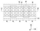
도 2는 도 1에서 A 영역을 확대하여 나타낸 평면도이다.
도 3은 도 2에서 III-III' 선을 따라 취한 단면의 일 실시예를 나타낸다.
도 4는 도 2에서 III-III' 선을 따라 취한 단면의 일 실시예를 나타낸다.
도 5는 도 2에서 III-III' 선을 따라 취한 단면의 일 실시예를 나타낸다.
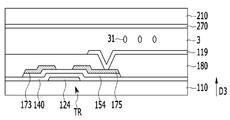
도 6은 도 1에서 A 영역의 단면의 일 실시예를 나타낸다.
도 7은 도 1에서 화소 영역의 단면의 일 실시예를 나타낸다.
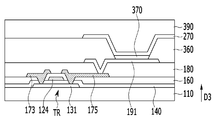
도 8은 도 1에서 A 영역의 단면의 일 실시예를 나타낸다.
도 9는 도 1에서 화소 영역의 단면의 일 실시예를 나타낸다.
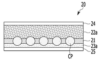
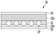
도 10은 본 발명의 일 실시예에 따른 이방성 도전 필름의 단면도이다.
도 11 내지 도 14는 도 10에 도시된 이방성 도전 필름을 제조하는 방법을 나타내는 공정 단면도이다.
도 15는 본 발명의 일 실시예에 따른 이방성 도전 필름의 단면도이다.
도 16은 본 발명의 일 실시예에 따른 이방성 도전 필름의 단면도이다.
도 17 및 도 18은 각각 본 발명의 일 실시예에 따른 도전 입자들의 배치를 나타낸 평면도이다.
129: 제1 도전층 179: 제2 도전층
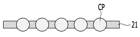
20: 이방성 도전 필름 21: 지지층
22: 제1 접착층 23: 제2 접착층
24: 제2 접착층 400: 집적회로 칩
50: 연성 인쇄회로기판 B: 범프
CP: 도전 입자 P: 패드
PP1: 제1 패드부 PP2: 제2 패드부
Claims (20)
- 기판 위에 위치하며 복수의 패드를 포함하는 패드부;
상기 패드부 위에 위치하는 이방성 도전 필름; 및
상기 이방성 도전 필름을 통해 상기 패드부에 부착되어 있으며, 복수의 범프를 포함하는 접속 부재;
를 포함하며,
상기 이방성 도전 필름은,
각각의 도전 입자의 일부분이 제1 면과 제2 면으로부터 돌출되어 있는 복수의 도전 입자를 포함하는 지지층;
상기 지지층의 상기 제1 면 및 상기 제1 면으로부터 돌출된 상기 도전 입자들의 부분과 접촉하는 제1 접착층; 및
상기 지지층의 상기 제2 면 및 상기 제2 면으로부터 돌출된 상기 도전 입자들의 부분과 접촉하는 제2 접착층;
을 포함하고, 상기 제1 접착층 및 상기 제2 접착층 중 적어도 하나는 상기 패드들과 상기 범퍼들이 중첩하는 제1 영역과 상기 패드들과 상기 범퍼들이 중첩하지 않는 제2 영역에 모두 위치하는 표시 장치. - 제1항에서,
상기 지지층은 상기 제1 접착층 및 상기 제2 접착층과 상이한 재료로 형성되어 있는 표시 장치. - 제2항에서,
상기 지지층은 폴리이미드, 폴리에틸렌 테레프탈레이트, 나일론 6, 폴리비닐리덴 플로라이드, 폴라카보네이트, 폴리부틸렌 숙시네이트 및 폴리에틸렌으로 이루어진 그룹에서 선택된 적어도 하나의 폴리머를 포함하는 표시 장치. - 제1항에서,
상기 지지층의 융점이 상기 제1 접착층의 경화점 및 상기 제2 접착층의 경화점보다 높은 표시 장치. - 제1항에서,
제1 방향으로 인접하는 도전 입자들 사이의 간격이 상기 제1 영역과 상기 제2 영역에서 일정한 표시 장치. - 제5항에서,
상기 제1 방향과 교차하는 제2 방향으로 인접하는 도전 입자들 사이의 간격이 상기 제1 영역과 상기 제2 영역에서 일정한 표시 장치. - 제5항에서,
상기 복수의 도전 입자는 평면도에서 장방형 또는 마름모형으로 배열되어 있는 표시 장치. - 제1항에서,
상기 복수의 도전 입자의 직경이 상기 지지층의 두께보다 큰 표시 장치. - 제1항에서,
상기 제1 접착층은 상기 제1 영역에 위치하는 부분의 두께가 상기 제2 영역에 위치하는 부분의 두께보다 작은 표시 장치. - 제1항에서,
상기 제2 접착층은 상기 제1 영역에 위치하는 부분의 두께가 상기 제2 영역에 위치하는 부분의 두께보다 작은 표시 장치. - 미경화 수지층에 도전 입자들을 배열하는 단계;
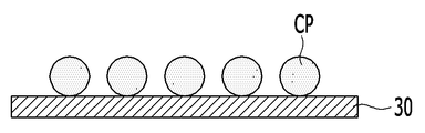
상기 수지층을 경화시켜 상기 도전 입자들을 경화된 수지층 내에 고정하는 단계; 및
상기 경화된 수지층을 식각하여 상기 도전 입자들의 일부분을 노출시키는 지지체를 형성하는 단계;
를 포함하는 이방성 도전 필름의 제조 방법. - 제11항에서,
상기 식각은 상기 지지체의 적어도 한 면에서 상기 도전 입자들의 일부분을 노출시키는 것을 포함하는 이방성 도전 필름의 제조 방법. - 제11항에서,
상기 식각은 반응성 이온 식각을 포함하는 이방성 도전 필름의 제조 방법. - 제11항에서,
상기 지지층은 폴리이미드, 폴리에틸렌 테레프탈레이트, 나일론 6, 폴리비닐리덴 플로라이드, 폴라카보네이트, 폴리부틸렌 숙시네이트 및 폴리에틸렌으로 이루어진 그룹에서 선택된 적어도 하나의 폴리머를 포함하는 이방성 도전 필름의 제조 방법. - 제11항에서,
상기 지지체의 상기 양면 중 적어도 한 면에 접착층을 형성하는 단계를 더 포함하는 이방성 도전 필름의 제조 방법. - 제15항에서,
상기 접착층은 상기 도전 입자들의 노출된 부분에 접촉하게 형성되는 이방성 도전 필름의 제조 방법. - 제15항에서,
상기 접착층은 상기 지지체 위에 미경화 수지층을 적층하여 형성되는 이방성 도전 필름의 형성 방법. - 제15항에서,
상기 접착층은 상기 지지층과 상이한 재료로 형성되는 이방성 도전 필름의 제조 방법. - 제15항에서,
상기 지지층의 융점이 상기 접착층의 경화점보다 높은 이방성 도전 필름의 제조 방법. - 제11항에서,
상기 지지층은 각각의 도전 입자의 직경보다 작은 두께로 형성되는 이방성 도전 필름의 제조 방법.
Priority Applications (3)
| Application Number | Priority Date | Filing Date | Title |
|---|---|---|---|
| KR1020160060271A KR20170130003A (ko) | 2016-05-17 | 2016-05-17 | 이방성 도전 필름을 포함하는 표시 장치 및 이방성 도전 필름의 제조 방법 |
| US15/365,979 US20170338198A1 (en) | 2016-05-17 | 2016-12-01 | Display device including an anisotropic conductive film, and manufacturing method of the anisotropic conductive film |
| CN201710342057.3A CN107393895A (zh) | 2016-05-17 | 2017-05-16 | 显示装置 |
Applications Claiming Priority (1)
| Application Number | Priority Date | Filing Date | Title |
|---|---|---|---|
| KR1020160060271A KR20170130003A (ko) | 2016-05-17 | 2016-05-17 | 이방성 도전 필름을 포함하는 표시 장치 및 이방성 도전 필름의 제조 방법 |
Publications (1)
| Publication Number | Publication Date |
|---|---|
| KR20170130003A true KR20170130003A (ko) | 2017-11-28 |
Family
ID=60330823
Family Applications (1)
| Application Number | Title | Priority Date | Filing Date |
|---|---|---|---|
| KR1020160060271A Ceased KR20170130003A (ko) | 2016-05-17 | 2016-05-17 | 이방성 도전 필름을 포함하는 표시 장치 및 이방성 도전 필름의 제조 방법 |
Country Status (3)
| Country | Link |
|---|---|
| US (1) | US20170338198A1 (ko) |
| KR (1) | KR20170130003A (ko) |
| CN (1) | CN107393895A (ko) |
Cited By (12)
| Publication number | Priority date | Publication date | Assignee | Title |
|---|---|---|---|---|
| KR101964881B1 (ko) * | 2018-01-17 | 2019-04-02 | 울산과학기술원 | 상온 액체 금속 캡슐을 이용하여 디바이스를 치유하는 신축성 패키지 및 이의 제조방법 |
| KR20190115163A (ko) * | 2018-03-30 | 2019-10-11 | 삼성디스플레이 주식회사 | 표시 장치 |
| KR20210043790A (ko) * | 2019-10-11 | 2021-04-22 | 삼성디스플레이 주식회사 | 접착 부재, 이를 포함한 표시장치, 및 표시장치의 제조 방법 |
| KR20210081019A (ko) * | 2019-12-23 | 2021-07-01 | 엘지디스플레이 주식회사 | 광경화성 수지로 형성된 고정층을 포함하는 이방성 도전 필름 및 이를 이용한 표시 장치 |
| KR20210090753A (ko) * | 2020-01-10 | 2021-07-21 | 삼성디스플레이 주식회사 | 표시패널, 표시패널의 제조 방법, 및 이를 포함한 표시장치 |
| KR20210114596A (ko) * | 2020-03-10 | 2021-09-24 | 삼성디스플레이 주식회사 | 표시장치 |
| US11145706B2 (en) | 2019-06-21 | 2021-10-12 | Samsung Display Co., Ltd. | Display device and method of manufacturing the same |
| US11209875B2 (en) | 2019-08-09 | 2021-12-28 | Samsung Display Co., Ltd. | Adhesive member and display device including the same |
| KR20220001527A (ko) * | 2020-06-29 | 2022-01-06 | 삼성디스플레이 주식회사 | 접착 부재 및 이를 포함하는 표시 장치 |
| US11419216B2 (en) | 2020-03-30 | 2022-08-16 | Samsung Display Co., Ltd. | Display device and method of manufacturing the same |
| US12058817B2 (en) | 2021-05-31 | 2024-08-06 | Samsung Display Co., Ltd. | Electronic device and method of manufacturing the same |
| US12249591B2 (en) | 2020-06-05 | 2025-03-11 | Samsung Display Co., Ltd. | Display device and method of manufacturing the same |
Families Citing this family (14)
| Publication number | Priority date | Publication date | Assignee | Title |
|---|---|---|---|---|
| US12550783B2 (en) * | 2016-05-17 | 2026-02-10 | Taiwan Semiconductor Manufacturing Company, Ltd. | Device and method for UBM/RDL routing |
| KR102487061B1 (ko) | 2016-06-30 | 2023-01-12 | 삼성디스플레이 주식회사 | 표시 장치 |
| JP2018054678A (ja) * | 2016-09-26 | 2018-04-05 | 株式会社ジャパンディスプレイ | 表示装置及びその製造方法 |
| CN108987439A (zh) * | 2018-06-21 | 2018-12-11 | 武汉华星光电半导体显示技术有限公司 | 显示面板和显示装置 |
| KR102629350B1 (ko) * | 2018-12-12 | 2024-01-25 | 삼성디스플레이 주식회사 | 표시 장치 및 그 제조 방법 |
| CN113823637B (zh) * | 2020-06-19 | 2024-05-10 | 元太科技工业股份有限公司 | 电子装置 |
| TWI730819B (zh) * | 2020-06-19 | 2021-06-11 | 元太科技工業股份有限公司 | 電子裝置 |
| KR20220014455A (ko) * | 2020-07-28 | 2022-02-07 | 삼성디스플레이 주식회사 | 표시 장치 및 표시 장치 제조 방법 |
| KR102876781B1 (ko) * | 2020-09-02 | 2025-10-27 | 삼성디스플레이 주식회사 | 타일형 표시 장치 |
| CN113451491B (zh) * | 2020-09-29 | 2022-04-29 | 重庆康佳光电技术研究院有限公司 | 显示面板及其制作方法 |
| US12074152B2 (en) * | 2020-11-06 | 2024-08-27 | Samsung Display Co., Ltd. | Display device |
| KR20220099200A (ko) * | 2021-01-05 | 2022-07-13 | 삼성디스플레이 주식회사 | 접착 부재, 표시 장치 및 표시 장치 제조 방법 |
| JP2023132391A (ja) * | 2022-03-11 | 2023-09-22 | イビデン株式会社 | プリント配線板 |
| CN117202726B (zh) * | 2023-09-13 | 2024-10-01 | 绵阳惠科光电科技有限公司 | 显示面板及其制备方法 |
Family Cites Families (7)
| Publication number | Priority date | Publication date | Assignee | Title |
|---|---|---|---|---|
| TW277152B (ko) * | 1994-05-10 | 1996-06-01 | Hitachi Chemical Co Ltd | |
| KR20070010015A (ko) * | 2004-03-30 | 2007-01-19 | 도카이 고무 고교 가부시키가이샤 | 이방성 도전막 및 그 제조방법 |
| JP2008027676A (ja) * | 2006-07-19 | 2008-02-07 | Tokai Rubber Ind Ltd | 異方性導電膜の製造方法および異方性導電膜 |
| KR101568659B1 (ko) * | 2013-03-29 | 2015-11-12 | 제일모직주식회사 | 도전성 접착층을 포함하는 이방 도전성 필름 및 상기 필름에 의해 접속된 반도체 장치 |
| JP6273875B2 (ja) * | 2014-02-04 | 2018-02-07 | デクセリアルズ株式会社 | 異方性導電フィルム及びその製造方法 |
| JP2015167106A (ja) * | 2014-03-04 | 2015-09-24 | 日立化成株式会社 | 異方導電性フィルム及び接続構造体 |
| WO2016068127A1 (ja) * | 2014-10-28 | 2016-05-06 | デクセリアルズ株式会社 | 異方導電性フィルム及び接続構造体 |
-
2016
- 2016-05-17 KR KR1020160060271A patent/KR20170130003A/ko not_active Ceased
- 2016-12-01 US US15/365,979 patent/US20170338198A1/en not_active Abandoned
-
2017
- 2017-05-16 CN CN201710342057.3A patent/CN107393895A/zh active Pending
Cited By (16)
| Publication number | Priority date | Publication date | Assignee | Title |
|---|---|---|---|---|
| KR101964881B1 (ko) * | 2018-01-17 | 2019-04-02 | 울산과학기술원 | 상온 액체 금속 캡슐을 이용하여 디바이스를 치유하는 신축성 패키지 및 이의 제조방법 |
| KR20230049076A (ko) * | 2018-03-30 | 2023-04-12 | 삼성디스플레이 주식회사 | 표시 장치 |
| KR20190115163A (ko) * | 2018-03-30 | 2019-10-11 | 삼성디스플레이 주식회사 | 표시 장치 |
| US11856828B2 (en) | 2019-06-21 | 2023-12-26 | Samsung Display Co., Ltd. | Display device and method of manufacturing the same |
| US11145706B2 (en) | 2019-06-21 | 2021-10-12 | Samsung Display Co., Ltd. | Display device and method of manufacturing the same |
| US11209875B2 (en) | 2019-08-09 | 2021-12-28 | Samsung Display Co., Ltd. | Adhesive member and display device including the same |
| KR20210043790A (ko) * | 2019-10-11 | 2021-04-22 | 삼성디스플레이 주식회사 | 접착 부재, 이를 포함한 표시장치, 및 표시장치의 제조 방법 |
| KR20210081019A (ko) * | 2019-12-23 | 2021-07-01 | 엘지디스플레이 주식회사 | 광경화성 수지로 형성된 고정층을 포함하는 이방성 도전 필름 및 이를 이용한 표시 장치 |
| KR20210090753A (ko) * | 2020-01-10 | 2021-07-21 | 삼성디스플레이 주식회사 | 표시패널, 표시패널의 제조 방법, 및 이를 포함한 표시장치 |
| US11824034B2 (en) | 2020-03-10 | 2023-11-21 | Samsung Display Co., Ltd. | Display device including adhesive film with conductive ball |
| KR20210114596A (ko) * | 2020-03-10 | 2021-09-24 | 삼성디스플레이 주식회사 | 표시장치 |
| US11419216B2 (en) | 2020-03-30 | 2022-08-16 | Samsung Display Co., Ltd. | Display device and method of manufacturing the same |
| KR20240134821A (ko) * | 2020-03-30 | 2024-09-10 | 삼성디스플레이 주식회사 | 표시 장치 및 표시 장치 제조 방법 |
| US12249591B2 (en) | 2020-06-05 | 2025-03-11 | Samsung Display Co., Ltd. | Display device and method of manufacturing the same |
| KR20220001527A (ko) * | 2020-06-29 | 2022-01-06 | 삼성디스플레이 주식회사 | 접착 부재 및 이를 포함하는 표시 장치 |
| US12058817B2 (en) | 2021-05-31 | 2024-08-06 | Samsung Display Co., Ltd. | Electronic device and method of manufacturing the same |
Also Published As
| Publication number | Publication date |
|---|---|
| CN107393895A (zh) | 2017-11-24 |
| US20170338198A1 (en) | 2017-11-23 |
Similar Documents
| Publication | Publication Date | Title |
|---|---|---|
| KR20170130003A (ko) | 이방성 도전 필름을 포함하는 표시 장치 및 이방성 도전 필름의 제조 방법 | |
| US8127438B2 (en) | Wiring substrate, method of manufacturing wiring substrate, and electronic apparatus | |
| CN101060205B (zh) | 平面显示面板及连接结构 | |
| US8497432B2 (en) | Electronic component mounting structure | |
| JP2000221540A (ja) | アクティブマトリクス型液晶表示装置 | |
| KR20170139217A (ko) | 표시장치 및 이의 제조방법 | |
| US20180011369A1 (en) | Display device having a connection member secured in place by a conductive layer | |
| JP5125314B2 (ja) | 電子装置 | |
| KR20000062451A (ko) | 영상 장치 및 그 제조 방법 | |
| US20220244603A1 (en) | Lcos structure and method of forming same | |
| JP3835460B2 (ja) | 電子部品実装体の製造方法、及び電気光学装置 | |
| KR20040050245A (ko) | 박막 트랜지스터 기판, 이의 제조방법, 이를 갖는액정표시장치 및 이의 제조방법 | |
| US12353100B2 (en) | Manufacturing method of an electronic device | |
| JP2018073246A (ja) | 表示装置 | |
| WO1999010928A1 (fr) | Dispositif semi-conducteur et procede de fabrication correspondant | |
| CN107665873B (zh) | 集成电路芯片及包括其的显示设备 | |
| KR102579426B1 (ko) | 표시 장치 및 그 제조 방법 | |
| CN114582221B (zh) | Tft阵列基板及包括其的显示面板 | |
| KR20260001003A (ko) | 연성 인쇄회로기판, 이를 포함하는 표시 장치, 및 연성 인쇄회로기판의 제조 방법 | |
| JP4844738B2 (ja) | 配線基板の製造方法 | |
| KR20250100888A (ko) | 표시 장치 | |
| JP2008118056A (ja) | 配線基板の製造方法および電子機器 | |
| JP2009049154A (ja) | 半導体装置、実装構造体、電気光学装置、電子機器 | |
| JPH06180459A (ja) | 液晶表示装置の実装構造及びその製造方法 | |
| JP2008159733A (ja) | 電子部品実装体の製造方法、電子部品実装体、及び、電気光学装置の製造方法 |
Legal Events
| Date | Code | Title | Description |
|---|---|---|---|
| PA0109 | Patent application |
St.27 status event code: A-0-1-A10-A12-nap-PA0109 |
|
| PG1501 | Laying open of application |
St.27 status event code: A-1-1-Q10-Q12-nap-PG1501 |
|
| R18-X000 | Changes to party contact information recorded |
St.27 status event code: A-3-3-R10-R18-oth-X000 |
|
| A201 | Request for examination | ||
| PA0201 | Request for examination |
St.27 status event code: A-1-2-D10-D11-exm-PA0201 |
|
| D13-X000 | Search requested |
St.27 status event code: A-1-2-D10-D13-srh-X000 |
|
| D14-X000 | Search report completed |
St.27 status event code: A-1-2-D10-D14-srh-X000 |
|
| PE0902 | Notice of grounds for rejection |
St.27 status event code: A-1-2-D10-D21-exm-PE0902 |
|
| AMND | Amendment | ||
| E13-X000 | Pre-grant limitation requested |
St.27 status event code: A-2-3-E10-E13-lim-X000 |
|
| P11-X000 | Amendment of application requested |
St.27 status event code: A-2-2-P10-P11-nap-X000 |
|
| P13-X000 | Application amended |
St.27 status event code: A-2-2-P10-P13-nap-X000 |
|
| P22-X000 | Classification modified |
St.27 status event code: A-2-2-P10-P22-nap-X000 |
|
| P22-X000 | Classification modified |
St.27 status event code: A-2-2-P10-P22-nap-X000 |
|
| E601 | Decision to refuse application | ||
| PE0601 | Decision on rejection of patent |
St.27 status event code: N-2-6-B10-B15-exm-PE0601 |
|
| AMND | Amendment | ||
| E13-X000 | Pre-grant limitation requested |
St.27 status event code: A-2-3-E10-E13-lim-X000 |
|
| P11-X000 | Amendment of application requested |
St.27 status event code: A-2-2-P10-P11-nap-X000 |
|
| P13-X000 | Application amended |
St.27 status event code: A-2-2-P10-P13-nap-X000 |
|
| PX0901 | Re-examination |
St.27 status event code: A-2-3-E10-E12-rex-PX0901 |
|
| PX0601 | Decision of rejection after re-examination |
St.27 status event code: N-2-6-B10-B17-rex-PX0601 |
|
| X601 | Decision of rejection after re-examination | ||
| P22-X000 | Classification modified |
St.27 status event code: A-2-2-P10-P22-nap-X000 |