KR20170132016A - Oled 표시 장치 및 그의 구동 방법 - Google Patents
Oled 표시 장치 및 그의 구동 방법 Download PDFInfo
- Publication number
- KR20170132016A KR20170132016A KR1020160062959A KR20160062959A KR20170132016A KR 20170132016 A KR20170132016 A KR 20170132016A KR 1020160062959 A KR1020160062959 A KR 1020160062959A KR 20160062959 A KR20160062959 A KR 20160062959A KR 20170132016 A KR20170132016 A KR 20170132016A
- Authority
- KR
- South Korea
- Prior art keywords
- node
- voltage
- gate electrode
- light emitting
- threshold voltage
- Prior art date
- Legal status (The legal status is an assumption and is not a legal conclusion. Google has not performed a legal analysis and makes no representation as to the accuracy of the status listed.)
- Granted
Links
Images


Classifications
-
- G—PHYSICS
- G09—EDUCATION; CRYPTOGRAPHY; DISPLAY; ADVERTISING; SEALS
- G09G—ARRANGEMENTS OR CIRCUITS FOR CONTROL OF INDICATING DEVICES USING STATIC MEANS TO PRESENT VARIABLE INFORMATION
- G09G3/00—Control arrangements or circuits, of interest only in connection with visual indicators other than cathode-ray tubes
- G09G3/20—Control arrangements or circuits, of interest only in connection with visual indicators other than cathode-ray tubes for presentation of an assembly of a number of characters, e.g. a page, by composing the assembly by combination of individual elements arranged in a matrix no fixed position being assigned to or needed to be assigned to the individual characters or partial characters
- G09G3/22—Control arrangements or circuits, of interest only in connection with visual indicators other than cathode-ray tubes for presentation of an assembly of a number of characters, e.g. a page, by composing the assembly by combination of individual elements arranged in a matrix no fixed position being assigned to or needed to be assigned to the individual characters or partial characters using controlled light sources
- G09G3/30—Control arrangements or circuits, of interest only in connection with visual indicators other than cathode-ray tubes for presentation of an assembly of a number of characters, e.g. a page, by composing the assembly by combination of individual elements arranged in a matrix no fixed position being assigned to or needed to be assigned to the individual characters or partial characters using controlled light sources using electroluminescent panels
- G09G3/32—Control arrangements or circuits, of interest only in connection with visual indicators other than cathode-ray tubes for presentation of an assembly of a number of characters, e.g. a page, by composing the assembly by combination of individual elements arranged in a matrix no fixed position being assigned to or needed to be assigned to the individual characters or partial characters using controlled light sources using electroluminescent panels semiconductive, e.g. using light-emitting diodes [LED]
- G09G3/3208—Control arrangements or circuits, of interest only in connection with visual indicators other than cathode-ray tubes for presentation of an assembly of a number of characters, e.g. a page, by composing the assembly by combination of individual elements arranged in a matrix no fixed position being assigned to or needed to be assigned to the individual characters or partial characters using controlled light sources using electroluminescent panels semiconductive, e.g. using light-emitting diodes [LED] organic, e.g. using organic light-emitting diodes [OLED]
- G09G3/3225—Control arrangements or circuits, of interest only in connection with visual indicators other than cathode-ray tubes for presentation of an assembly of a number of characters, e.g. a page, by composing the assembly by combination of individual elements arranged in a matrix no fixed position being assigned to or needed to be assigned to the individual characters or partial characters using controlled light sources using electroluminescent panels semiconductive, e.g. using light-emitting diodes [LED] organic, e.g. using organic light-emitting diodes [OLED] using an active matrix
- G09G3/3258—Control arrangements or circuits, of interest only in connection with visual indicators other than cathode-ray tubes for presentation of an assembly of a number of characters, e.g. a page, by composing the assembly by combination of individual elements arranged in a matrix no fixed position being assigned to or needed to be assigned to the individual characters or partial characters using controlled light sources using electroluminescent panels semiconductive, e.g. using light-emitting diodes [LED] organic, e.g. using organic light-emitting diodes [OLED] using an active matrix with pixel circuitry controlling the voltage across the light-emitting element
-
- G—PHYSICS
- G09—EDUCATION; CRYPTOGRAPHY; DISPLAY; ADVERTISING; SEALS
- G09G—ARRANGEMENTS OR CIRCUITS FOR CONTROL OF INDICATING DEVICES USING STATIC MEANS TO PRESENT VARIABLE INFORMATION
- G09G3/00—Control arrangements or circuits, of interest only in connection with visual indicators other than cathode-ray tubes
- G09G3/20—Control arrangements or circuits, of interest only in connection with visual indicators other than cathode-ray tubes for presentation of an assembly of a number of characters, e.g. a page, by composing the assembly by combination of individual elements arranged in a matrix no fixed position being assigned to or needed to be assigned to the individual characters or partial characters
- G09G3/22—Control arrangements or circuits, of interest only in connection with visual indicators other than cathode-ray tubes for presentation of an assembly of a number of characters, e.g. a page, by composing the assembly by combination of individual elements arranged in a matrix no fixed position being assigned to or needed to be assigned to the individual characters or partial characters using controlled light sources
- G09G3/30—Control arrangements or circuits, of interest only in connection with visual indicators other than cathode-ray tubes for presentation of an assembly of a number of characters, e.g. a page, by composing the assembly by combination of individual elements arranged in a matrix no fixed position being assigned to or needed to be assigned to the individual characters or partial characters using controlled light sources using electroluminescent panels
- G09G3/32—Control arrangements or circuits, of interest only in connection with visual indicators other than cathode-ray tubes for presentation of an assembly of a number of characters, e.g. a page, by composing the assembly by combination of individual elements arranged in a matrix no fixed position being assigned to or needed to be assigned to the individual characters or partial characters using controlled light sources using electroluminescent panels semiconductive, e.g. using light-emitting diodes [LED]
- G09G3/3208—Control arrangements or circuits, of interest only in connection with visual indicators other than cathode-ray tubes for presentation of an assembly of a number of characters, e.g. a page, by composing the assembly by combination of individual elements arranged in a matrix no fixed position being assigned to or needed to be assigned to the individual characters or partial characters using controlled light sources using electroluminescent panels semiconductive, e.g. using light-emitting diodes [LED] organic, e.g. using organic light-emitting diodes [OLED]
- G09G3/3225—Control arrangements or circuits, of interest only in connection with visual indicators other than cathode-ray tubes for presentation of an assembly of a number of characters, e.g. a page, by composing the assembly by combination of individual elements arranged in a matrix no fixed position being assigned to or needed to be assigned to the individual characters or partial characters using controlled light sources using electroluminescent panels semiconductive, e.g. using light-emitting diodes [LED] organic, e.g. using organic light-emitting diodes [OLED] using an active matrix
- G09G3/3233—Control arrangements or circuits, of interest only in connection with visual indicators other than cathode-ray tubes for presentation of an assembly of a number of characters, e.g. a page, by composing the assembly by combination of individual elements arranged in a matrix no fixed position being assigned to or needed to be assigned to the individual characters or partial characters using controlled light sources using electroluminescent panels semiconductive, e.g. using light-emitting diodes [LED] organic, e.g. using organic light-emitting diodes [OLED] using an active matrix with pixel circuitry controlling the current through the light-emitting element
-
- G—PHYSICS
- G09—EDUCATION; CRYPTOGRAPHY; DISPLAY; ADVERTISING; SEALS
- G09G—ARRANGEMENTS OR CIRCUITS FOR CONTROL OF INDICATING DEVICES USING STATIC MEANS TO PRESENT VARIABLE INFORMATION
- G09G3/00—Control arrangements or circuits, of interest only in connection with visual indicators other than cathode-ray tubes
- G09G3/20—Control arrangements or circuits, of interest only in connection with visual indicators other than cathode-ray tubes for presentation of an assembly of a number of characters, e.g. a page, by composing the assembly by combination of individual elements arranged in a matrix no fixed position being assigned to or needed to be assigned to the individual characters or partial characters
- G09G3/22—Control arrangements or circuits, of interest only in connection with visual indicators other than cathode-ray tubes for presentation of an assembly of a number of characters, e.g. a page, by composing the assembly by combination of individual elements arranged in a matrix no fixed position being assigned to or needed to be assigned to the individual characters or partial characters using controlled light sources
- G09G3/30—Control arrangements or circuits, of interest only in connection with visual indicators other than cathode-ray tubes for presentation of an assembly of a number of characters, e.g. a page, by composing the assembly by combination of individual elements arranged in a matrix no fixed position being assigned to or needed to be assigned to the individual characters or partial characters using controlled light sources using electroluminescent panels
- G09G3/32—Control arrangements or circuits, of interest only in connection with visual indicators other than cathode-ray tubes for presentation of an assembly of a number of characters, e.g. a page, by composing the assembly by combination of individual elements arranged in a matrix no fixed position being assigned to or needed to be assigned to the individual characters or partial characters using controlled light sources using electroluminescent panels semiconductive, e.g. using light-emitting diodes [LED]
- G09G3/3208—Control arrangements or circuits, of interest only in connection with visual indicators other than cathode-ray tubes for presentation of an assembly of a number of characters, e.g. a page, by composing the assembly by combination of individual elements arranged in a matrix no fixed position being assigned to or needed to be assigned to the individual characters or partial characters using controlled light sources using electroluminescent panels semiconductive, e.g. using light-emitting diodes [LED] organic, e.g. using organic light-emitting diodes [OLED]
- G09G3/3275—Details of drivers for data electrodes
- G09G3/3291—Details of drivers for data electrodes in which the data driver supplies a variable data voltage for setting the current through, or the voltage across, the light-emitting elements
-
- H—ELECTRICITY
- H10—SEMICONDUCTOR DEVICES; ELECTRIC SOLID-STATE DEVICES NOT OTHERWISE PROVIDED FOR
- H10D—INORGANIC ELECTRIC SEMICONDUCTOR DEVICES
- H10D30/00—Field-effect transistors [FET]
- H10D30/60—Insulated-gate field-effect transistors [IGFET]
- H10D30/67—Thin-film transistors [TFT]
- H10D30/6729—Thin-film transistors [TFT] characterised by the electrodes
- H10D30/673—Thin-film transistors [TFT] characterised by the electrodes characterised by the shapes, relative sizes or dispositions of the gate electrodes
- H10D30/6733—Multi-gate TFTs
- H10D30/6734—Multi-gate TFTs having gate electrodes arranged on both top and bottom sides of the channel, e.g. dual-gate TFTs
-
- H—ELECTRICITY
- H10—SEMICONDUCTOR DEVICES; ELECTRIC SOLID-STATE DEVICES NOT OTHERWISE PROVIDED FOR
- H10D—INORGANIC ELECTRIC SEMICONDUCTOR DEVICES
- H10D86/00—Integrated devices formed in or on insulating or conducting substrates, e.g. formed in silicon-on-insulator [SOI] substrates or on stainless steel or glass substrates
- H10D86/40—Integrated devices formed in or on insulating or conducting substrates, e.g. formed in silicon-on-insulator [SOI] substrates or on stainless steel or glass substrates characterised by multiple TFTs
- H10D86/421—Integrated devices formed in or on insulating or conducting substrates, e.g. formed in silicon-on-insulator [SOI] substrates or on stainless steel or glass substrates characterised by multiple TFTs having a particular composition, shape or crystalline structure of the active layer
- H10D86/423—Integrated devices formed in or on insulating or conducting substrates, e.g. formed in silicon-on-insulator [SOI] substrates or on stainless steel or glass substrates characterised by multiple TFTs having a particular composition, shape or crystalline structure of the active layer comprising semiconductor materials not belonging to the Group IV, e.g. InGaZnO
-
- H—ELECTRICITY
- H10—SEMICONDUCTOR DEVICES; ELECTRIC SOLID-STATE DEVICES NOT OTHERWISE PROVIDED FOR
- H10D—INORGANIC ELECTRIC SEMICONDUCTOR DEVICES
- H10D86/00—Integrated devices formed in or on insulating or conducting substrates, e.g. formed in silicon-on-insulator [SOI] substrates or on stainless steel or glass substrates
- H10D86/40—Integrated devices formed in or on insulating or conducting substrates, e.g. formed in silicon-on-insulator [SOI] substrates or on stainless steel or glass substrates characterised by multiple TFTs
- H10D86/481—Integrated devices formed in or on insulating or conducting substrates, e.g. formed in silicon-on-insulator [SOI] substrates or on stainless steel or glass substrates characterised by multiple TFTs integrated with passive devices, e.g. auxiliary capacitors
-
- H—ELECTRICITY
- H10—SEMICONDUCTOR DEVICES; ELECTRIC SOLID-STATE DEVICES NOT OTHERWISE PROVIDED FOR
- H10D—INORGANIC ELECTRIC SEMICONDUCTOR DEVICES
- H10D86/00—Integrated devices formed in or on insulating or conducting substrates, e.g. formed in silicon-on-insulator [SOI] substrates or on stainless steel or glass substrates
- H10D86/40—Integrated devices formed in or on insulating or conducting substrates, e.g. formed in silicon-on-insulator [SOI] substrates or on stainless steel or glass substrates characterised by multiple TFTs
- H10D86/60—Integrated devices formed in or on insulating or conducting substrates, e.g. formed in silicon-on-insulator [SOI] substrates or on stainless steel or glass substrates characterised by multiple TFTs wherein the TFTs are in active matrices
-
- H—ELECTRICITY
- H10—SEMICONDUCTOR DEVICES; ELECTRIC SOLID-STATE DEVICES NOT OTHERWISE PROVIDED FOR
- H10K—ORGANIC ELECTRIC SOLID-STATE DEVICES
- H10K59/00—Integrated devices, or assemblies of multiple devices, comprising at least one organic light-emitting element covered by group H10K50/00
- H10K59/10—OLED displays
- H10K59/12—Active-matrix OLED [AMOLED] displays
- H10K59/121—Active-matrix OLED [AMOLED] displays characterised by the geometry or disposition of pixel elements
- H10K59/1213—Active-matrix OLED [AMOLED] displays characterised by the geometry or disposition of pixel elements the pixel elements being TFTs
-
- H—ELECTRICITY
- H10—SEMICONDUCTOR DEVICES; ELECTRIC SOLID-STATE DEVICES NOT OTHERWISE PROVIDED FOR
- H10K—ORGANIC ELECTRIC SOLID-STATE DEVICES
- H10K59/00—Integrated devices, or assemblies of multiple devices, comprising at least one organic light-emitting element covered by group H10K50/00
- H10K59/10—OLED displays
- H10K59/12—Active-matrix OLED [AMOLED] displays
- H10K59/121—Active-matrix OLED [AMOLED] displays characterised by the geometry or disposition of pixel elements
- H10K59/1216—Active-matrix OLED [AMOLED] displays characterised by the geometry or disposition of pixel elements the pixel elements being capacitors
-
- G—PHYSICS
- G09—EDUCATION; CRYPTOGRAPHY; DISPLAY; ADVERTISING; SEALS
- G09G—ARRANGEMENTS OR CIRCUITS FOR CONTROL OF INDICATING DEVICES USING STATIC MEANS TO PRESENT VARIABLE INFORMATION
- G09G2300/00—Aspects of the constitution of display devices
- G09G2300/08—Active matrix structure, i.e. with use of active elements, inclusive of non-linear two terminal elements, in the pixels together with light emitting or modulating elements
- G09G2300/0809—Several active elements per pixel in active matrix panels
- G09G2300/0842—Several active elements per pixel in active matrix panels forming a memory circuit, e.g. a dynamic memory with one capacitor
- G09G2300/0852—Several active elements per pixel in active matrix panels forming a memory circuit, e.g. a dynamic memory with one capacitor being a dynamic memory with more than one capacitor
-
- G—PHYSICS
- G09—EDUCATION; CRYPTOGRAPHY; DISPLAY; ADVERTISING; SEALS
- G09G—ARRANGEMENTS OR CIRCUITS FOR CONTROL OF INDICATING DEVICES USING STATIC MEANS TO PRESENT VARIABLE INFORMATION
- G09G2300/00—Aspects of the constitution of display devices
- G09G2300/08—Active matrix structure, i.e. with use of active elements, inclusive of non-linear two terminal elements, in the pixels together with light emitting or modulating elements
- G09G2300/0809—Several active elements per pixel in active matrix panels
- G09G2300/0842—Several active elements per pixel in active matrix panels forming a memory circuit, e.g. a dynamic memory with one capacitor
- G09G2300/0861—Several active elements per pixel in active matrix panels forming a memory circuit, e.g. a dynamic memory with one capacitor with additional control of the display period without amending the charge stored in a pixel memory, e.g. by means of additional select electrodes
-
- G—PHYSICS
- G09—EDUCATION; CRYPTOGRAPHY; DISPLAY; ADVERTISING; SEALS
- G09G—ARRANGEMENTS OR CIRCUITS FOR CONTROL OF INDICATING DEVICES USING STATIC MEANS TO PRESENT VARIABLE INFORMATION
- G09G2300/00—Aspects of the constitution of display devices
- G09G2300/08—Active matrix structure, i.e. with use of active elements, inclusive of non-linear two terminal elements, in the pixels together with light emitting or modulating elements
- G09G2300/0809—Several active elements per pixel in active matrix panels
- G09G2300/0871—Several active elements per pixel in active matrix panels with level shifting
-
- G—PHYSICS
- G09—EDUCATION; CRYPTOGRAPHY; DISPLAY; ADVERTISING; SEALS
- G09G—ARRANGEMENTS OR CIRCUITS FOR CONTROL OF INDICATING DEVICES USING STATIC MEANS TO PRESENT VARIABLE INFORMATION
- G09G2310/00—Command of the display device
- G09G2310/02—Addressing, scanning or driving the display screen or processing steps related thereto
- G09G2310/0262—The addressing of the pixel, in a display other than an active matrix LCD, involving the control of two or more scan electrodes or two or more data electrodes, e.g. pixel voltage dependent on signals of two data electrodes
-
- G—PHYSICS
- G09—EDUCATION; CRYPTOGRAPHY; DISPLAY; ADVERTISING; SEALS
- G09G—ARRANGEMENTS OR CIRCUITS FOR CONTROL OF INDICATING DEVICES USING STATIC MEANS TO PRESENT VARIABLE INFORMATION
- G09G2310/00—Command of the display device
- G09G2310/08—Details of timing specific for flat panels, other than clock recovery
-
- G—PHYSICS
- G09—EDUCATION; CRYPTOGRAPHY; DISPLAY; ADVERTISING; SEALS
- G09G—ARRANGEMENTS OR CIRCUITS FOR CONTROL OF INDICATING DEVICES USING STATIC MEANS TO PRESENT VARIABLE INFORMATION
- G09G2320/00—Control of display operating conditions
- G09G2320/02—Improving the quality of display appearance
- G09G2320/0233—Improving the luminance or brightness uniformity across the screen
-
- G—PHYSICS
- G09—EDUCATION; CRYPTOGRAPHY; DISPLAY; ADVERTISING; SEALS
- G09G—ARRANGEMENTS OR CIRCUITS FOR CONTROL OF INDICATING DEVICES USING STATIC MEANS TO PRESENT VARIABLE INFORMATION
- G09G2320/00—Control of display operating conditions
- G09G2320/02—Improving the quality of display appearance
- G09G2320/0257—Reduction of after-image effects
-
- G—PHYSICS
- G09—EDUCATION; CRYPTOGRAPHY; DISPLAY; ADVERTISING; SEALS
- G09G—ARRANGEMENTS OR CIRCUITS FOR CONTROL OF INDICATING DEVICES USING STATIC MEANS TO PRESENT VARIABLE INFORMATION
- G09G2320/00—Control of display operating conditions
- G09G2320/04—Maintaining the quality of display appearance
- G09G2320/043—Preventing or counteracting the effects of ageing
-
- H—ELECTRICITY
- H10—SEMICONDUCTOR DEVICES; ELECTRIC SOLID-STATE DEVICES NOT OTHERWISE PROVIDED FOR
- H10D—INORGANIC ELECTRIC SEMICONDUCTOR DEVICES
- H10D86/00—Integrated devices formed in or on insulating or conducting substrates, e.g. formed in silicon-on-insulator [SOI] substrates or on stainless steel or glass substrates
- H10D86/40—Integrated devices formed in or on insulating or conducting substrates, e.g. formed in silicon-on-insulator [SOI] substrates or on stainless steel or glass substrates characterised by multiple TFTs
Landscapes
- Engineering & Computer Science (AREA)
- Physics & Mathematics (AREA)
- Computer Hardware Design (AREA)
- General Physics & Mathematics (AREA)
- Theoretical Computer Science (AREA)
- Geometry (AREA)
- Microelectronics & Electronic Packaging (AREA)
- Electroluminescent Light Sources (AREA)
- Control Of El Displays (AREA)
- Control Of Indicators Other Than Cathode Ray Tubes (AREA)
Abstract
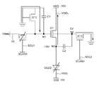
또한, OLED 표시장치의 화소 구동 회로는 제2 및 제3 스위칭 소자(ST2, ST3)를 턴-온시켜, 제1 노드(N1)에는 음의 문턱전압(-Vth)이 인가 되고, 제2 노드(N2)는 0V로 초기화하는 초기화 기간, 제3 스위칭 소자(ST3)와 구동 스위칭 소자(DT)를 턴-온시켜, 제3 노드(N3)에 음의 문턱전압의 두 배가 인가되고, 제2 커패시터(C2)에 두 배의 문턱전압(2Vth)이 저장되는 샘플링 기간, 제1 스위칭 소자(ST1)는 턴-온 시키고, 제2 및 제3 스위칭 소자(ST2, ST3)는 턴-오프 시켜, 제1 노드(N1)에 데이터 전압(Vdata)이 인가되고, 제3 노드(N3)에 유기발광소자 전압(VOLED)이 충전되고, 제2 노드(N2)는 유기발광소자 전압과 두 배의 문턱전압이 더해진 전압으로 부스팅(Boosting)되는 프로그래밍 기간 및 제1와 제2 스위칭 소자(ST1, ST2)를 턴-오프 시켜 제1 스위칭 소자(ST1)로부터 유입된 데이터 신호에 대응하여, 구동 스위칭 소자(DT)가 유기발광소자에 구동 전류를 공급하는 발광 기간으로 구분하여 동작하는 것을 특징으로 한다.
Description
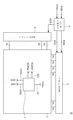
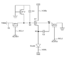
도 2는 본 발명의 실시 예에 따른 도1에 도시된 화소의 회로도 이다.
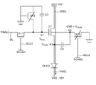
도 3는 본 발명의 실시 예에 따른 도 1에 도시된 화소의 구동 파형도 이다.
도 4a 내지 도 4d는 본 발명의 일 실시 예에 따른 도 3에 도시된 구동 파형도의 구간 별 신호 흐름을 나타내는 회로도 이다.
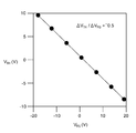
도 5a 및 도 5b는 본 발명의 실시 예에 따른 도 2에 도시된 구동 트랜지스터의 상부 게이트 전극에 인가되는 전압과 문턱전압 관계를 보여주는 그래프이다.
도 6은 본 발명의 실시 예에 따른 도 2에 도시된 구동 트랜지스터의 단면도이다.

3: 데이터 드라이버 4: 게이트 드라이버
5: 타이밍 컨트롤러 110: 기판
120: 하부 게이트 전극(BG) 130: 게이트 절연층
140: 활성화층 150A, 150B: 소스 및 드레인 전극
160: 보호층 170: 상부 게이트 전극(TG)
C1: 저장 커패시터 C2: 보상 커패시터(Ccomp)
ST1:제1 스위칭 트랜지스터, 제1 스위칭 소자
ST2: 제2 스위칭 트랜지스터, 제2 스위칭 소자
ST3: 보상 트랜지스터(CT), 제3 스위칭 소자
DT: 구동 트랜지스터, 구동 스위칭 소자
Claims (33)
- 유기발광 소자;
상기 유기발광 소자의 구동에 관여하고, 하부 게이트 전극(BG), 옥사이드 반도체 층, 소스 전극, 드레인 전극 및 상부 게이트 전극(TG)을 포함하는 구동 트랜지스터;
상기 구동 트랜지스터의 하부 게이트 전극에 전기적으로 연결되어, 상기 구동 트랜지스터의 제어에 필요한 데이터 전압(Vdata) 전송에 관여하는 제1 스위칭 트랜지스터;
상기 하부 게이트 전극과 전기적으로 연결되며, 데이터 전압의 충전에 관여하는 저장 커패시터(Cst);
상기 저장 커패시터에 문턱전압(Vth)을 저장하는 제2 스위칭 트랜지스터;
상기 구동 트랜지스터의 상부 게이트 전극과 직접 연결되어, 상기 구동 트랜지스터의 문턱전압 편차를 보상하는 보상 트랜지스터; 및
상기 구동 트랜지스터의 소스 전극과 상기 보상 트랜지스터의 소스 전극 사이에 형성되어 문턱전압이 저장된 보상 커패시터(Ccomp)를 포함하는 유기발광 표시장치. - 제1항에 있어서,
상기 게이트 절연층의 두께는 상기 구동 트랜지스터의 문턱전압을 보상하는 보상값에 의해 제어되는 것을 특징으로 하는 유기발광 표시장치. - 제1항에 있어서,
상기 제1 스위칭 트랜지스터는 제1 게이트 전극, 제1 옥사이드 반도체 층, 제1 소스 전극 및 제1 드레인 전극을 구비하고, 상기 제1 소스 전극은 상기 구동 트랜지스터의 하부 게이트 전극과 접속된 제1노드(N1)와 직접 연결되는 것을 특징으로 하는 유기발광 표시장치. - 제1항에 있어서,
상기 제2 스위칭 트랜지스터는 제2 게이트 전극, 제2 옥사이드 반도체 층, 제2 소스 전극 및 제3 드레인 전극을 구비하고, 상기 제2 게이트 전극과 상기 제2 드레인 전극은 공통으로 접지되고, 상기 저장 커패시터(Cst)의 일 전극은 상기 접지와 연결되는 것을 특징으로 하는 유기발광 표시장치. - 제3항에 있어서,
상기 저장 커패시터(Cst)의 다른 전극은 상기 제1노드(N1) 및 상기 제1 스위칭 트랜지스터의 소스 전극과 연결되는 것을 특징으로 하는 유기발광 표시장치. - 제1항에 있어서,
상기 보상 트랜지스터는 제3 게이트 전극, 제3 옥사이드 반도체 층, 제3 소스 전극 및 제3 드레인 전극을 구비하고, 상기 제3 소스 전극은 상기 구동 트랜지스터의 상부 게이트 전극과 접속된 제2 노드(N2)와 직접 연결되는 것을 특징으로 하는 유기발광 표시장치. - 제1항에 있어서,
상기 구동 트랜지스터의 상기 드레인 전극은 제1 전원 공급 라인(VDDL)과 전기적으로 연결되어 있으며,
상기 구동 트랜지스터의 상기 소스 전극은 제3 노드(N3)와 연결되어 있는 것을 특징으로 하는 유기발광 표시장치. - 제 3항 및 6항 중 어느 하나에 있어서,
상기 제2 스위칭 트랜지스터와 상기 보상 트랜지스터가 턴-온(Turn-On) 시, 상기 제2 스위칭 트랜지스터의 음(negative)의 문턱전압(-Vth)이 상기 제1 노드(N1)에 인가되고, 상기 제2 노드(N2)는 0V가 인가 되는 것을 특징으로 하는 유기발광 표시장치. - 제 7항에 있어서,
상기 제2 스위칭 트랜지스터는 턴-오프(Turn-Off)가 되고, 상기 보상 트랜지스터가 턴-온 시, 상기 제3 노드(N3)에는 음의 문턱전압의 두 배가 인가되는 것을 특징으로 하는 유기발광 표시장치. - 제 7항에 있어서,
상기 제1 스위칭 트랜지스터는 턴-온이 되고, 상기 보상 트랜지스터가 턴-오프 시, 상기 유기발광소자는 온(On)이 되고, 상기 제3 노드(N3)에는 상기 유기발광소자에 걸리는 전압(VOLED)이 인가되는 것을 특징으로 하는 유기발광 표시장치. - 제 6항에 있어서,
상기 보상 트랜지스터가 턴 오프(Turn-off)일 때, 상기 제2 노드(N2)는 플로팅(Floating) 상태인 것을 특징으로 하는 유기발광 표시장치. - 제 10항에 있어서,
상기 제2 노드(N2)는 상기 보상 커패시터에 저장된 두 배의 문턱전압(2Vth)을 유지하기 위하여 상기 유기발광소자의 온(On) 전압(VOLED)과 상기 구동 트랜지스터의 상기 두 배의 문턱전압이 더해진 전압으로 부스팅(Boosting)되어 인가되는 것을 특징으로 하는 유기발광 표시장치. - 제 12항에 있어서,
상기 제2 노드(N2) 및 제3 노드(N3)사이의 양단 전압이 상기 두 배의 문턱전압으로 유지되어, 상기 구동 트랜지스터의 상부 게이트 전극에 인가되는 전압이 상기 구동 트랜지스터의 문턱전압을 제어하는 것을 특징으로 하는 유기발광 표시장치. - 하부 게이트 전극과 상부 게이트 전극을 구비하고, 제1 전원 공급라인(VDDL)과 제2 전원 공급라인(VSSL)에 전기적으로 연결된 구동 스위칭 소자(DT);
제1 스캔신호(SCAN1)에 대응하여, 데이터 신호 라인(DL)과 상기 구동 스위칭 소자(DT)의 하부 게이트 전극에 접속된 제1 노드(N1)를 서로 전기적으로 연결 시키는 제1 스위칭 소자(ST1);
상기 제1 노드와 연결되고, 게이트 전극과 드레인 전극이 공통으로 접지되는 다이오드 연결 형태의 제2 스위칭 소자(ST2);
제2 스캔신호(SCAN2)에 대응하여, 접지단과 상기 구동 스위칭 소자(DT)의 상부 게이트 전극에 접속된 제2 노드(N2)를 서로 전기적으로 연결 시키는 제3 스위칭 소자(ST3);
상기 제1 노드(N1) 및 상기 제2 스위칭 소자(ST2) 사이에 전기적으로 연결된 제1 커패시터(C1); 및
상기 제2 노드(N2) 및 상기 구동 스위칭 소자(DT)의 소스 전극에 접속된 제3 노드(N3) 사이에 전기적으로 연결된 제2 커패시터(C2)를 포함하는 화소 구동회로. - 제14항에 있어서,
상기 제1 스위칭 소자(ST1)는 제1 게이트 전극, 제1 옥사이드 반도체 층, 제1 소스 전극 및 제1 드레인 전극을 구비하고, 상기 제1 게이트 전극은 상기 제1 스캔신호(SCAN1)를 공급하는 제1 스캔신호 라인(SCL1)과 연결된 것을 특징으로 하는 화소 구동회로. - 제 15항에 있어서,
상기 제1 드레인 전극은 상기 데이터 신호 라인(DL)과 연결되어 데이터 전압(Vdata)을 공급받는 것을 특징으로 하는 화소 구동회로. - 제 14항에 있어서,
상기 제3 스위칭 소자(ST3)는 제3 게이트 전극, 제3 옥사이드 반도체 층, 제3 소스 전극 및 제3 드레인 전극을 구비하고, 상기 제3 게이트 전극은 상기 제2 스캔신호(SCAN2)를 공급하는 제2 스캔신호 라인(SCL2)과 연결된 것을 특징으로 하는 화소 구동회로. - 제 17항에 있어서,
상기 제3 드레인 전극은 상기 접지단과 연결되는 것을 특징으로 하는 화소 구동회로. - 제 14항에 있어서,
상기 제2 노드(N2)는 상기 제3 스위칭 소자(ST3)가 턴-오프 되면, 상기 접지단에 의해 전위차가 없는 플로팅(Floating) 상태가 되는 것을 특징으로 하는 화소 구동회로. - 제14항에 있어서,
상기 제2 스위칭 소자(ST2)는 제2 게이트 전극, 제2 옥사이드 반도체 층, 제2 소스 전극 및 제2 드레인 전극을 구비하고, 상기 제2 소스 전극은 상기 제1 노드(N1) 및 상기 제1 스위칭 소자(ST1)의 소스 전극과 연결되고, 상기 드레인 전극은 상기 제1 커패시터(C1)의 일 전극과 연결되는 것을 특징으로 하는 화소 구동회로. - 제20항에 있어서,
상기 제1 커패시터(C1)의 다른 전극은 상기 제1 노드(N1) 및 상기 제1 스위칭 소자(ST1)의 소스 전극과 연결되는 것을 특징으로 하는 화소 구동회로. - 제14항에 있어서,
상기 제2 커패시터(C2)는 두 배의 문턱전압(2Vth)을 저장하는 것을 특징으로 하는 화소 구동회로. - 제22항에 있어서,
상기 제2 노드(N2) 및 제3 노드(N3)사이의 양단 전압이 상기 두 배의 문턱전압(2Vth)으로 유지되어, 상기 상부 게이트 전극에 인가된 전압이 상기 구동 트랜지스터의 문턱전압(Vth)을 제어하는 것을 특징으로 하는 화소 구동회로. - 제23항에 있어서,
상기 상부 게이트 전극에 상기 구동 트랜지스터(DT)의 문턱전압(Vth)의 두 배에 해당하는 전압이 인가되고, 상기 구동 트랜지스터(DT)의 문턱전압은 일 배의 문턱전압(Vth)으로 낮아지는 것을 특징으로 하는 화소 구동회로. - 복수 화소 각각이 유기발광 소자와, 상기 유기발광 소자를 구동하는 화소 구동 회로를 구비하고,
상기 화소 구동 회로는
하부 게이트 전극과 상부 게이트 전극을 구비하고, 상기 유기발광소자와 함께 제1 전원 공급라인(VDDL)과 제2 전원 공급 라인(VSSL) 사이에 직렬로 연결된 구동 스위칭 소자(DT);
제1 스캔 신호에 대응하여 데이터 신호 라인(DL)과 상기 구동 스위칭 소자의 하부 게이트 전극에 접속된 제1 노드(N1)를 서로 연결하는 제1 스위칭 소자(ST1);
상기 제1 노드와 연결되고, 제2 게이트 전극과 제2 드레인 전극이 공통으로 접지되는 다이오드 연결 형태의 제2 스위칭 소자(ST2);
제2 스캔 신호에 대응하여 접지단과 상기 구동 스위칭 소자의 상부 게이트 전극에 접속된 제2노드(N2)를 서로 연결하는 제3 스위칭 소자(ST3);
상기 제1 노드(N1) 및 상기 제2 스위칭 소자(ST2) 사이에 전기적으로 연결된 제1 커패시터(C1); 및
상기 제2 노드 및 상기 구동 스위칭 소자의 드레인에 접속된 제3 노드(N3) 사이에 위치하는 제2 커패시터(C2)를 구비하고,
상기 화소 구동 회로는
상기 제2 및 제3 스위칭 소자(ST2, ST3)를 턴-온시켜, 상기 제1 노드(N1)에는 음의 문턱전압(-Vth)이 인가 되고, 상기 제2 노드(N2)는 0V로 초기화하는 초기화 기간;
상기 제3 스위칭 소자(ST3)와 상기 구동 스위칭 소자(DT)를 턴-온시켜, 상기 제3 노드(N3)에 음의 문턱전압의 두 배가 인가되고, 상기 제2 커패시터(C2)에 두 배의 문턱전압(2Vth)이 저장되는 샘플링 기간;
상기 제1 스위칭 소자(ST1)는 턴-온 시키고, 상기 제2 및 제3 스위칭 소자(ST2, ST3)는 턴-오프 시켜, 상기 제1 노드(N1)에 데이터 전압(Vdata)이 인가되고, 상기 제3 노드(N3)에 유기발광소자 전압(VOLED)이 충전되고, 상기 제2 노드(N2)는 상기 유기발광소자 전압(VOLED)과 상기 두 배의 문턱전압(2Vth)이 더해진 전압으로 부스팅(Boosting)되는 프로그래밍 기간; 및
상기 제1 및 제2 스위칭 소자(ST1, ST2)를 턴-오프 시켜 상기 제1 스위칭 소자(ST1)로부터 유입된 데이터 신호에 대응하여, 상기 구동 스위칭 소자(DT)가 상기 유기발광소자에 구동 전류를 공급하는 발광 기간으로 구분하여 동작하는 것을 특징으로 하는 OLED 표시장치. - 제25항에 있어서,
상기 초기화 기간에서, 상기 제2 게이트 전극과 상기 제2 드레인 전극은 공통으로 접지되어 다이오드 연결 상태가 되고, 상기 제1 노드(N1)에 상기 음의 문턱전압(-Vth)이 공급되어, 상기 제1 커패시터(C1)를 문턱전압(Vth)으로 초기화 시키는 것을 특징으로 하는 OLED 표시장치. - 제25항에 있어서,
상기 초기화 기간에서, 상기 제2 스위칭 소자(ST2)가 턴-온 되고, 상기 접지 단으로부터 0V가 상기 제2 노드(N2)에 공급되어, 상기 제2 커패시터(C2)를 방전시키는 것을 특징으로 하는 OLED 표시장치. - 제25항에 있어서,
상기 샘플링 기간에서, 상기 제3 노드(N3)는 상기 구동 스위칭 소자(DT)의 게이트-소스 전압(Vgs)이 문턱전압(Vth)이 될 때까지 상기 음의 문턱전압(-Vth)의 두 배로 충전되며, 상기 제3 노드(N3)에 상기 음의 문턱전압(-Vth)의 두 배가 인가되면 상기 구동 스위칭 소자(DT)를 턴-오프 시키는 것을 특징으로 하는 OLED 표시장치. - 제25항에 있어서,
상기 샘플링 기간에서, 상기 제2 커패시터(C2)에 상기 두 배의 문턱전압(2Vth)이 충전되고, 상기 유기발광소자에 상기 제2 전원 공급라인(VSSL)으로부터 하이 레벨 전압이 인가되어 상기 유기발광소자가 발광하지 않는 것을 특징으로 하는 OLED 표시장치. - 제25항에 있어서,
상기 프로그래밍 기간에서, 상기 제2 전원 공급라인(VSSL)에 로우 레벨 전압이 인가되어, 상기 유기발광소자는 턴-온 되며, 상기 제3 노드(N3)에 상기 유기발광소자 전압(VOLED)이 인가되는 것을 특징으로 하는 OLED 표시장치. - 제25항에 있어서,
상기 프로그래밍 기간에서,
상기 제3 스위칭 소자(ST3)의 턴-오프에 의해 상기 제2 노드가 플로팅(floating) 상태가 되며,
상기 제2 커패시터에 상기 두 배의 문턱전압(2Vth)을 유지하기 위하여 상기 제2 노드의 전압이 0V에서 상기 유기발광소자 전압(VOLED)과 상기 두 배의 문턱전압(2Vth)이 더해진 전압으로 부스팅(Boosting)되는 것을 특징으로 하는 OLED 표시장치. - 제25항에 있어서,
상기 상부 게이트 전극에 인가 되는 전압에 의해 상기 구동 스위칭 소자의 문턱전압(Vth)을 조절하는 것을 특징으로 하는 OLED 표시장치. - 제25항에 있어서,
상기 샘플링 구간에, 상기 구동 스위칭 소자의 문턱전압(Vth)이 부극성인 경우에도 센싱(sensing)이 되는 것을 특징으로 하는 OLED 표시장치.
Priority Applications (3)
| Application Number | Priority Date | Filing Date | Title |
|---|---|---|---|
| KR1020160062959A KR102570832B1 (ko) | 2016-05-23 | 2016-05-23 | Oled 표시 장치 및 그의 구동 방법 |
| US15/598,887 US10366656B2 (en) | 2016-05-23 | 2017-05-18 | Organic light-emitting diode display device and method of driving the same |
| CN201710368630.8A CN107424563B (zh) | 2016-05-23 | 2017-05-23 | 有机发光二极管显示装置 |
Applications Claiming Priority (1)
| Application Number | Priority Date | Filing Date | Title |
|---|---|---|---|
| KR1020160062959A KR102570832B1 (ko) | 2016-05-23 | 2016-05-23 | Oled 표시 장치 및 그의 구동 방법 |
Publications (2)
| Publication Number | Publication Date |
|---|---|
| KR20170132016A true KR20170132016A (ko) | 2017-12-01 |
| KR102570832B1 KR102570832B1 (ko) | 2023-08-24 |
Family
ID=60330356
Family Applications (1)
| Application Number | Title | Priority Date | Filing Date |
|---|---|---|---|
| KR1020160062959A Active KR102570832B1 (ko) | 2016-05-23 | 2016-05-23 | Oled 표시 장치 및 그의 구동 방법 |
Country Status (3)
| Country | Link |
|---|---|
| US (1) | US10366656B2 (ko) |
| KR (1) | KR102570832B1 (ko) |
| CN (1) | CN107424563B (ko) |
Cited By (12)
| Publication number | Priority date | Publication date | Assignee | Title |
|---|---|---|---|---|
| KR20190064998A (ko) * | 2017-12-01 | 2019-06-11 | 엘지디스플레이 주식회사 | 게이트 드라이버와 이를 포함한 표시장치 |
| KR20200000513A (ko) * | 2018-06-22 | 2020-01-03 | 삼성디스플레이 주식회사 | 유기 발광 표시 장치 |
| KR20200129242A (ko) * | 2019-05-07 | 2020-11-18 | 삼성디스플레이 주식회사 | 화소 회로 및 이를 포함하는 표시 장치 |
| KR20210035936A (ko) * | 2019-09-24 | 2021-04-02 | 삼성디스플레이 주식회사 | 화소 회로 및 이를 포함하는 표시 장치 |
| KR20210132789A (ko) * | 2020-04-27 | 2021-11-05 | 삼성디스플레이 주식회사 | 표시 장치 |
| KR20220086012A (ko) * | 2020-12-16 | 2022-06-23 | 주식회사 엘엑스세미콘 | 소스드라이버 집적회로 |
| US11551593B2 (en) | 2020-07-09 | 2023-01-10 | Samsung Display Co., Ltd. | Organic light-emitting diode display device performing a sensing operation, and method of sensing degradation of an organic light-emitting diode display device |
| US11798476B2 (en) | 2021-07-08 | 2023-10-24 | Lg Display Co., Ltd. | Pixel circuit and display device including the same |
| KR20240077442A (ko) * | 2022-11-24 | 2024-05-31 | 한양대학교 에리카산학협력단 | 픽셀 회로, 이를 이용한 표시장치 및 이의 제조방법 |
| US12008948B2 (en) | 2021-05-31 | 2024-06-11 | Samsung Display Co., Ltd. | Display device |
| US12347365B2 (en) | 2022-11-24 | 2025-07-01 | Industry-University Cooperation Foundation Hanyang University Erica Campus | Pixel circuit, display device using the same and manufacturing method thereof |
| WO2026010320A1 (ko) * | 2024-07-04 | 2026-01-08 | 삼성디스플레이 주식회사 | 표시 장치 및 이를 포함하는 전자 장치 |
Families Citing this family (46)
| Publication number | Priority date | Publication date | Assignee | Title |
|---|---|---|---|---|
| KR102518914B1 (ko) * | 2015-09-23 | 2023-04-07 | 삼성디스플레이 주식회사 | 화소 및 이를 포함하는 유기 발광 표시 장치 |
| CN106782330B (zh) * | 2016-12-20 | 2019-03-12 | 上海天马有机发光显示技术有限公司 | 有机发光像素驱动电路、驱动方法以及有机发光显示面板 |
| CN107093403B (zh) * | 2017-06-30 | 2019-03-15 | 深圳市华星光电技术有限公司 | 用于oled显示面板的像素驱动电路的补偿方法 |
| JP6935055B2 (ja) * | 2017-07-21 | 2021-09-15 | 天馬微電子有限公司 | Oled表示装置、その回路、及びその製造方法 |
| CN107358915B (zh) * | 2017-08-11 | 2020-01-07 | 上海天马有机发光显示技术有限公司 | 一种像素电路、其驱动方法、显示面板及显示装置 |
| CN107767814B (zh) * | 2017-11-27 | 2020-02-21 | 合肥鑫晟光电科技有限公司 | 像素电路、显示装置和双栅驱动晶体管 |
| KR102563660B1 (ko) | 2018-01-15 | 2023-08-08 | 삼성디스플레이 주식회사 | 화소 및 이를 갖는 유기발광 표시장치 |
| CN111919246B (zh) * | 2018-03-27 | 2022-07-26 | 夏普株式会社 | 显示装置 |
| CN110459172B (zh) | 2018-05-08 | 2020-06-09 | 京东方科技集团股份有限公司 | 一种像素驱动电路及驱动方法、显示装置 |
| US10490128B1 (en) * | 2018-06-05 | 2019-11-26 | Apple Inc. | Electronic devices having low refresh rate display pixels with reduced sensitivity to oxide transistor threshold voltage |
| CN110070825B (zh) * | 2018-06-14 | 2020-10-09 | 友达光电股份有限公司 | 像素电路 |
| CN108777131B (zh) * | 2018-06-22 | 2020-04-03 | 武汉华星光电半导体显示技术有限公司 | Amoled像素驱动电路及驱动方法 |
| KR102565412B1 (ko) * | 2018-08-28 | 2023-08-10 | 삼성디스플레이 주식회사 | 유기 발광 표시 장치 |
| WO2020053693A1 (ja) * | 2018-09-12 | 2020-03-19 | 株式会社半導体エネルギー研究所 | 表示装置の動作方法 |
| CN118675469A (zh) | 2018-09-13 | 2024-09-20 | 京东方科技集团股份有限公司 | 像素电路及其驱动方法、显示装置 |
| US12120915B2 (en) * | 2018-09-18 | 2024-10-15 | Sharp Kabushiki Kaisha | Display device with driving transistor having upper and lower gate electrodes |
| KR102631125B1 (ko) * | 2018-10-30 | 2024-01-29 | 엘지디스플레이 주식회사 | 화소 및 이를 포함하는 발광 표시 장치 |
| CN111199712A (zh) * | 2018-11-16 | 2020-05-26 | 上海和辉光电有限公司 | 像素补偿电路及显示装置 |
| KR102531674B1 (ko) * | 2018-12-31 | 2023-05-12 | 삼성디스플레이 주식회사 | 표시 패널 |
| CN109637435B (zh) * | 2019-01-21 | 2021-03-26 | 惠科股份有限公司 | 一种显示面板的驱动电路、驱动方法及显示装置 |
| CN110288947A (zh) * | 2019-06-28 | 2019-09-27 | 京东方科技集团股份有限公司 | 一种像素电路及其驱动方法、显示装置 |
| CN110570816B (zh) * | 2019-09-11 | 2021-03-09 | 合肥京东方卓印科技有限公司 | 像素电路及其驱动方法 |
| CN114467134B (zh) * | 2019-10-02 | 2024-04-09 | 夏普株式会社 | 显示装置 |
| KR102706520B1 (ko) * | 2019-11-21 | 2024-09-11 | 엘지디스플레이 주식회사 | 스트레쳐블 표시 장치 |
| CN111210765B (zh) | 2020-02-14 | 2022-02-11 | 华南理工大学 | 像素电路、像素电路的驱动方法和显示面板 |
| US10916197B1 (en) * | 2020-02-14 | 2021-02-09 | Shenzhen China Star Optoelectronics Semiconductor Display Technology Co., Ltd. | Pixel compensation circuit and display panel |
| CN111354322A (zh) * | 2020-04-08 | 2020-06-30 | 深圳市华星光电半导体显示技术有限公司 | 一种同步发光的像素补偿电路及显示面板 |
| CN111402788A (zh) * | 2020-04-08 | 2020-07-10 | 深圳市华星光电半导体显示技术有限公司 | 一种像素电路和显示面板 |
| CN111429836A (zh) | 2020-04-09 | 2020-07-17 | 深圳市华星光电半导体显示技术有限公司 | 一种像素驱动电路和显示面板 |
| KR102765748B1 (ko) * | 2020-04-21 | 2025-02-13 | 삼성디스플레이 주식회사 | 표시 장치 |
| US11138924B1 (en) * | 2020-07-03 | 2021-10-05 | Innolux Corporation | Driving circuit for driving a light emitting unit |
| KR102825010B1 (ko) * | 2020-09-25 | 2025-06-27 | 삼성디스플레이 주식회사 | 게이트 구동 회로 및 이를 포함하는 표시 장치 |
| KR102803136B1 (ko) * | 2020-10-29 | 2025-05-07 | 엘지디스플레이 주식회사 | 표시장치 및 그 구동방법 |
| KR102718076B1 (ko) * | 2020-12-15 | 2024-10-15 | 엘지디스플레이 주식회사 | 표시장치 및 그 구동방법 |
| KR20220111820A (ko) * | 2021-02-02 | 2022-08-10 | 삼성디스플레이 주식회사 | 픽셀 및 이를 포함하는 표시 장치 |
| CN112927652A (zh) * | 2021-02-05 | 2021-06-08 | 深圳市华星光电半导体显示技术有限公司 | 像素电路及其驱动方法、显示面板和显示装置 |
| TWI828189B (zh) * | 2021-07-08 | 2024-01-01 | 南韓商Lg顯示器股份有限公司 | 像素電路及包含該像素電路的顯示裝置 |
| KR102869885B1 (ko) * | 2021-12-02 | 2025-10-13 | 엘지디스플레이 주식회사 | 디스플레이 장치 |
| KR102896461B1 (ko) * | 2021-12-21 | 2025-12-04 | 엘지디스플레이 주식회사 | 표시 장치 |
| KR20230105745A (ko) * | 2022-01-04 | 2023-07-12 | 삼성디스플레이 주식회사 | 표시 장치 |
| CN114550656B (zh) * | 2022-03-02 | 2022-12-02 | 绵阳惠科光电科技有限公司 | 驱动电路、驱动装置以及显示装置 |
| CN117276280A (zh) * | 2022-06-13 | 2023-12-22 | 京东方科技集团股份有限公司 | 一种显示基板、其制作方法及显示装置 |
| CN115223494B (zh) * | 2022-07-18 | 2024-01-30 | 深圳市华星光电半导体显示技术有限公司 | 驱动电路及显示面板 |
| WO2025059912A1 (zh) * | 2023-09-20 | 2025-03-27 | 京东方科技集团股份有限公司 | 显示基板和显示装置 |
| KR20250071957A (ko) * | 2023-11-15 | 2025-05-23 | 삼성디스플레이 주식회사 | 표시 장치 및 이를 이용한 표시 장치의 구동 방법 |
| WO2026083215A1 (ja) * | 2024-10-18 | 2026-04-23 | 株式会社半導体エネルギー研究所 | 半導体装置 |
Citations (4)
| Publication number | Priority date | Publication date | Assignee | Title |
|---|---|---|---|---|
| US20130063413A1 (en) * | 2011-09-14 | 2013-03-14 | Semiconductor Energy Laboratory Co., Ltd. | Light-emitting device |
| US20130069068A1 (en) * | 2011-09-16 | 2013-03-21 | Semiconductor Energy Laboratory Co., Ltd. | Semiconductor device, light-emitting device, and electronic device |
| US20140168194A1 (en) * | 2012-12-17 | 2014-06-19 | Lg Display Co., Ltd. | Organic light emitting display |
| US20160042694A1 (en) * | 2014-08-07 | 2016-02-11 | Samsung Display Co., Ltd. | Pixel circuit and organic light-emitting diode display including the same |
Family Cites Families (8)
| Publication number | Priority date | Publication date | Assignee | Title |
|---|---|---|---|---|
| JP5152448B2 (ja) | 2004-09-21 | 2013-02-27 | カシオ計算機株式会社 | 画素駆動回路及び画像表示装置 |
| JP4479755B2 (ja) | 2007-07-03 | 2010-06-09 | ソニー株式会社 | 有機エレクトロルミネッセンス素子、及び、有機エレクトロルミネッセンス表示装置 |
| CN102820001A (zh) | 2011-06-07 | 2012-12-12 | 东莞万士达液晶显示器有限公司 | 有机发光二极管像素电路 |
| CN102629447B (zh) | 2011-10-21 | 2014-06-11 | 京东方科技集团股份有限公司 | 像素电路及其补偿方法 |
| JP5780650B2 (ja) | 2011-11-11 | 2015-09-16 | 株式会社Joled | レベルシフタ回路、走査回路、表示装置、及び、電子機器 |
| TWI463467B (zh) | 2012-02-22 | 2014-12-01 | Chunghwa Picture Tubes Ltd | 亮度均勻的雙閘極液晶顯示器 |
| CN102915703B (zh) | 2012-10-30 | 2014-12-17 | 京东方科技集团股份有限公司 | 一种像素驱动电路及其驱动方法 |
| CN104732927B (zh) | 2015-04-09 | 2017-10-03 | 京东方科技集团股份有限公司 | 一种像素电路及其驱动方法和显示装置 |
-
2016
- 2016-05-23 KR KR1020160062959A patent/KR102570832B1/ko active Active
-
2017
- 2017-05-18 US US15/598,887 patent/US10366656B2/en active Active
- 2017-05-23 CN CN201710368630.8A patent/CN107424563B/zh active Active
Patent Citations (6)
| Publication number | Priority date | Publication date | Assignee | Title |
|---|---|---|---|---|
| US20130063413A1 (en) * | 2011-09-14 | 2013-03-14 | Semiconductor Energy Laboratory Co., Ltd. | Light-emitting device |
| US20130069068A1 (en) * | 2011-09-16 | 2013-03-21 | Semiconductor Energy Laboratory Co., Ltd. | Semiconductor device, light-emitting device, and electronic device |
| US20140168194A1 (en) * | 2012-12-17 | 2014-06-19 | Lg Display Co., Ltd. | Organic light emitting display |
| KR20140078419A (ko) * | 2012-12-17 | 2014-06-25 | 엘지디스플레이 주식회사 | 유기발광 표시장치 |
| US20160042694A1 (en) * | 2014-08-07 | 2016-02-11 | Samsung Display Co., Ltd. | Pixel circuit and organic light-emitting diode display including the same |
| KR20160018892A (ko) * | 2014-08-07 | 2016-02-18 | 삼성디스플레이 주식회사 | 화소 회로 및 이를 포함하는 유기 발광 표시 장치 |
Cited By (18)
| Publication number | Priority date | Publication date | Assignee | Title |
|---|---|---|---|---|
| KR20190064998A (ko) * | 2017-12-01 | 2019-06-11 | 엘지디스플레이 주식회사 | 게이트 드라이버와 이를 포함한 표시장치 |
| KR20200000513A (ko) * | 2018-06-22 | 2020-01-03 | 삼성디스플레이 주식회사 | 유기 발광 표시 장치 |
| US11881172B2 (en) | 2019-05-07 | 2024-01-23 | Samsung Display Co., Ltd. | Pixel circuit and display device including the same |
| KR20200129242A (ko) * | 2019-05-07 | 2020-11-18 | 삼성디스플레이 주식회사 | 화소 회로 및 이를 포함하는 표시 장치 |
| US12367828B2 (en) | 2019-05-07 | 2025-07-22 | Samsung Display Co., Ltd. | Pixel circuit and display device including the same |
| KR20210035936A (ko) * | 2019-09-24 | 2021-04-02 | 삼성디스플레이 주식회사 | 화소 회로 및 이를 포함하는 표시 장치 |
| CN112634830A (zh) * | 2019-09-24 | 2021-04-09 | 三星显示有限公司 | 像素电路及包括像素电路的显示装置 |
| US12249284B2 (en) | 2019-09-24 | 2025-03-11 | Samsung Display Co., Ltd. | Pixel circuit and display device including the same |
| KR20210132789A (ko) * | 2020-04-27 | 2021-11-05 | 삼성디스플레이 주식회사 | 표시 장치 |
| US12243456B2 (en) | 2020-07-09 | 2025-03-04 | Samsung Display Co., Ltd. | Organic light-emitting diode display device performing a sensing operation, and method of sensing degradation of an organic light-emitting diode display device |
| US11551593B2 (en) | 2020-07-09 | 2023-01-10 | Samsung Display Co., Ltd. | Organic light-emitting diode display device performing a sensing operation, and method of sensing degradation of an organic light-emitting diode display device |
| KR20220086012A (ko) * | 2020-12-16 | 2022-06-23 | 주식회사 엘엑스세미콘 | 소스드라이버 집적회로 |
| US12008948B2 (en) | 2021-05-31 | 2024-06-11 | Samsung Display Co., Ltd. | Display device |
| US11798476B2 (en) | 2021-07-08 | 2023-10-24 | Lg Display Co., Ltd. | Pixel circuit and display device including the same |
| US12260820B2 (en) | 2021-07-08 | 2025-03-25 | Lg Display Co., Ltd. | Pixel circuit and display device including the same |
| KR20240077442A (ko) * | 2022-11-24 | 2024-05-31 | 한양대학교 에리카산학협력단 | 픽셀 회로, 이를 이용한 표시장치 및 이의 제조방법 |
| US12347365B2 (en) | 2022-11-24 | 2025-07-01 | Industry-University Cooperation Foundation Hanyang University Erica Campus | Pixel circuit, display device using the same and manufacturing method thereof |
| WO2026010320A1 (ko) * | 2024-07-04 | 2026-01-08 | 삼성디스플레이 주식회사 | 표시 장치 및 이를 포함하는 전자 장치 |
Also Published As
| Publication number | Publication date |
|---|---|
| CN107424563B (zh) | 2020-02-18 |
| KR102570832B1 (ko) | 2023-08-24 |
| CN107424563A (zh) | 2017-12-01 |
| US10366656B2 (en) | 2019-07-30 |
| US20170337875A1 (en) | 2017-11-23 |
Similar Documents
| Publication | Publication Date | Title |
|---|---|---|
| KR102570832B1 (ko) | Oled 표시 장치 및 그의 구동 방법 | |
| US10551903B2 (en) | Organic light emitting display apparatus | |
| US10930728B2 (en) | Organic light-emitting diode display and method of manufacturing the same | |
| KR102623352B1 (ko) | 유기발광표시장치 및 그의 구동방법 | |
| US9105213B2 (en) | Organic light emitting diode display and method of driving the same | |
| KR100986915B1 (ko) | 유기전계발광 표시장치 및 그의 구동방법 | |
| US9647047B2 (en) | Organic light emitting display for initializing pixels | |
| KR101040786B1 (ko) | 화소 및 이를 이용한 유기전계발광 표시장치 | |
| US9189991B2 (en) | Organic light emitting display device having pixels and method of driving the same | |
| KR101765778B1 (ko) | 유기전계발광 표시장치 | |
| US9262962B2 (en) | Pixel and organic light emitting display device using the same | |
| KR20170122432A (ko) | Oled 표시 장치 및 그의 구동 방법 | |
| US10157580B2 (en) | Organic light emitting display having data driver supplying sensing data voltage in a sensing mode | |
| US20100141645A1 (en) | Organic light emitting display device and method of driving the same | |
| KR20180003387A (ko) | 유기발광 표시장치 및 그의 구동 방법 | |
| KR102348765B1 (ko) | 유기발광 표시장치의 발광소자에 대한 열화 센싱 방법 | |
| JP5284492B2 (ja) | 表示装置及びその制御方法 | |
| US9491829B2 (en) | Organic light emitting diode display and method of driving the same | |
| KR20160008705A (ko) | 화소 및 이를 이용한 유기전계발광 표시장치 | |
| CN108470541B (zh) | 像素电路及其驱动方法、显示面板及显示装置 | |
| US12603052B2 (en) | Pixel circuit and electroluminescent display apparatus including the same | |
| KR101907959B1 (ko) | 유기 발광 다이오드 표시장치 | |
| KR20120000434A (ko) | 유기전계발광표시장치 및 그 구동방법 | |
| KR101699045B1 (ko) | 유기 전계발광 표시장치 및 그의 구동방법 | |
| KR102330584B1 (ko) | 유기발광 표시장치 |
Legal Events
| Date | Code | Title | Description |
|---|---|---|---|
| PA0109 | Patent application |
Patent event code: PA01091R01D Comment text: Patent Application Patent event date: 20160523 |
|
| PG1501 | Laying open of application | ||
| A201 | Request for examination | ||
| PA0201 | Request for examination |
Patent event code: PA02012R01D Patent event date: 20210524 Comment text: Request for Examination of Application Patent event code: PA02011R01I Patent event date: 20160523 Comment text: Patent Application |
|
| E902 | Notification of reason for refusal | ||
| PE0902 | Notice of grounds for rejection |
Comment text: Notification of reason for refusal Patent event date: 20220728 Patent event code: PE09021S01D |
|
| E701 | Decision to grant or registration of patent right | ||
| PE0701 | Decision of registration |
Patent event code: PE07011S01D Comment text: Decision to Grant Registration Patent event date: 20230607 |
|
| GRNT | Written decision to grant | ||
| PR0701 | Registration of establishment |
Comment text: Registration of Establishment Patent event date: 20230822 Patent event code: PR07011E01D |
|
| PR1002 | Payment of registration fee |
Payment date: 20230822 End annual number: 3 Start annual number: 1 |
|
| PG1601 | Publication of registration |