KR20170136109A - 색변환 패널 및 이를 포함하는 표시 장치 - Google Patents
색변환 패널 및 이를 포함하는 표시 장치 Download PDFInfo
- Publication number
- KR20170136109A KR20170136109A KR1020160067303A KR20160067303A KR20170136109A KR 20170136109 A KR20170136109 A KR 20170136109A KR 1020160067303 A KR1020160067303 A KR 1020160067303A KR 20160067303 A KR20160067303 A KR 20160067303A KR 20170136109 A KR20170136109 A KR 20170136109A
- Authority
- KR
- South Korea
- Prior art keywords
- layer
- color conversion
- polarizing
- substrate
- display panel
- Prior art date
- Legal status (The legal status is an assumption and is not a legal conclusion. Google has not performed a legal analysis and makes no representation as to the accuracy of the status listed.)
- Ceased
Links
- 238000006243 chemical reaction Methods 0.000 title claims abstract description 157
- 239000000758 substrate Substances 0.000 claims abstract description 80
- 230000010287 polarization Effects 0.000 claims abstract description 51
- 239000002096 quantum dot Substances 0.000 claims abstract description 31
- 239000004973 liquid crystal related substance Substances 0.000 claims description 55
- 230000003287 optical effect Effects 0.000 claims description 41
- 229910052751 metal Inorganic materials 0.000 claims description 37
- 239000002184 metal Substances 0.000 claims description 37
- 238000000034 method Methods 0.000 claims description 24
- VYPSYNLAJGMNEJ-UHFFFAOYSA-N Silicium dioxide Chemical compound O=[Si]=O VYPSYNLAJGMNEJ-UHFFFAOYSA-N 0.000 claims description 14
- 229910052814 silicon oxide Inorganic materials 0.000 claims description 10
- 229910052581 Si3N4 Inorganic materials 0.000 claims description 5
- 239000007769 metal material Substances 0.000 claims description 5
- HQVNEWCFYHHQES-UHFFFAOYSA-N silicon nitride Chemical compound N12[Si]34N5[Si]62N3[Si]51N64 HQVNEWCFYHHQES-UHFFFAOYSA-N 0.000 claims description 5
- 229910052804 chromium Inorganic materials 0.000 claims description 4
- 229910044991 metal oxide Inorganic materials 0.000 claims description 4
- 150000004706 metal oxides Chemical class 0.000 claims description 4
- 229910052750 molybdenum Inorganic materials 0.000 claims description 4
- 229910052719 titanium Inorganic materials 0.000 claims description 4
- 229910052782 aluminium Inorganic materials 0.000 claims description 3
- 229910052802 copper Inorganic materials 0.000 claims description 3
- 229910052737 gold Inorganic materials 0.000 claims description 3
- 229910052709 silver Inorganic materials 0.000 claims description 3
- 230000005540 biological transmission Effects 0.000 abstract description 22
- 239000010410 layer Substances 0.000 description 516
- 239000010408 film Substances 0.000 description 39
- 239000000463 material Substances 0.000 description 16
- 150000001875 compounds Chemical class 0.000 description 14
- 230000001681 protective effect Effects 0.000 description 14
- 239000004065 semiconductor Substances 0.000 description 11
- 239000000203 mixture Substances 0.000 description 10
- OAICVXFJPJFONN-UHFFFAOYSA-N Phosphorus Chemical compound [P] OAICVXFJPJFONN-UHFFFAOYSA-N 0.000 description 9
- 230000000903 blocking effect Effects 0.000 description 8
- 230000000052 comparative effect Effects 0.000 description 8
- 230000005684 electric field Effects 0.000 description 8
- 230000002452 interceptive effect Effects 0.000 description 8
- 239000010409 thin film Substances 0.000 description 8
- 230000001066 destructive effect Effects 0.000 description 7
- 238000002834 transmittance Methods 0.000 description 7
- 229910004205 SiNX Inorganic materials 0.000 description 5
- 238000002310 reflectometry Methods 0.000 description 5
- -1 silane compound Chemical class 0.000 description 5
- 239000011248 coating agent Substances 0.000 description 4
- 238000000576 coating method Methods 0.000 description 4
- 238000002347 injection Methods 0.000 description 4
- 239000007924 injection Substances 0.000 description 4
- 229910052788 barium Inorganic materials 0.000 description 3
- 229910052791 calcium Inorganic materials 0.000 description 3
- 239000004020 conductor Substances 0.000 description 3
- 239000002245 particle Substances 0.000 description 3
- 239000011347 resin Substances 0.000 description 3
- 229920005989 resin Polymers 0.000 description 3
- 229910000077 silane Inorganic materials 0.000 description 3
- 229910052712 strontium Inorganic materials 0.000 description 3
- 229910018072 Al 2 O 3 Inorganic materials 0.000 description 2
- 229910017083 AlN Inorganic materials 0.000 description 2
- 229910019923 CrOx Inorganic materials 0.000 description 2
- 229910003564 SiAlON Inorganic materials 0.000 description 2
- 229910006404 SnO 2 Inorganic materials 0.000 description 2
- 229910010413 TiO 2 Inorganic materials 0.000 description 2
- 229910003087 TiOx Inorganic materials 0.000 description 2
- 238000010521 absorption reaction Methods 0.000 description 2
- JNDMLEXHDPKVFC-UHFFFAOYSA-N aluminum;oxygen(2-);yttrium(3+) Chemical group [O-2].[O-2].[O-2].[Al+3].[Y+3] JNDMLEXHDPKVFC-UHFFFAOYSA-N 0.000 description 2
- 230000000694 effects Effects 0.000 description 2
- 229910021480 group 4 element Inorganic materials 0.000 description 2
- 239000011810 insulating material Substances 0.000 description 2
- 238000004519 manufacturing process Methods 0.000 description 2
- 239000011159 matrix material Substances 0.000 description 2
- 230000004048 modification Effects 0.000 description 2
- 238000012986 modification Methods 0.000 description 2
- 239000002105 nanoparticle Substances 0.000 description 2
- 238000000206 photolithography Methods 0.000 description 2
- 239000000377 silicon dioxide Substances 0.000 description 2
- HLLICFJUWSZHRJ-UHFFFAOYSA-N tioxidazole Chemical compound CCCOC1=CC=C2N=C(NC(=O)OC)SC2=C1 HLLICFJUWSZHRJ-UHFFFAOYSA-N 0.000 description 2
- 229910019901 yttrium aluminum garnet Inorganic materials 0.000 description 2
- YBNMDCCMCLUHBL-UHFFFAOYSA-N (2,5-dioxopyrrolidin-1-yl) 4-pyren-1-ylbutanoate Chemical compound C=1C=C(C2=C34)C=CC3=CC=CC4=CC=C2C=1CCCC(=O)ON1C(=O)CCC1=O YBNMDCCMCLUHBL-UHFFFAOYSA-N 0.000 description 1
- 229910017115 AlSb Inorganic materials 0.000 description 1
- PIGFYZPCRLYGLF-UHFFFAOYSA-N Aluminum nitride Chemical compound [Al]#N PIGFYZPCRLYGLF-UHFFFAOYSA-N 0.000 description 1
- 229910004613 CdTe Inorganic materials 0.000 description 1
- 229910004611 CdZnTe Inorganic materials 0.000 description 1
- 229910002601 GaN Inorganic materials 0.000 description 1
- 229910005540 GaP Inorganic materials 0.000 description 1
- 229910005542 GaSb Inorganic materials 0.000 description 1
- 229910001218 Gallium arsenide Inorganic materials 0.000 description 1
- 229910004262 HgTe Inorganic materials 0.000 description 1
- 229910000673 Indium arsenide Inorganic materials 0.000 description 1
- GPXJNWSHGFTCBW-UHFFFAOYSA-N Indium phosphide Chemical compound [In]#P GPXJNWSHGFTCBW-UHFFFAOYSA-N 0.000 description 1
- 241000764773 Inna Species 0.000 description 1
- 229910000661 Mercury cadmium telluride Inorganic materials 0.000 description 1
- 229910015711 MoOx Inorganic materials 0.000 description 1
- 229910002665 PbTe Inorganic materials 0.000 description 1
- 229910004283 SiO 4 Inorganic materials 0.000 description 1
- 229910000577 Silicon-germanium Inorganic materials 0.000 description 1
- 229910005642 SnTe Inorganic materials 0.000 description 1
- ATJFFYVFTNAWJD-UHFFFAOYSA-N Tin Chemical compound [Sn] ATJFFYVFTNAWJD-UHFFFAOYSA-N 0.000 description 1
- 229910007709 ZnTe Inorganic materials 0.000 description 1
- UHYPYGJEEGLRJD-UHFFFAOYSA-N cadmium(2+);selenium(2-) Chemical compound [Se-2].[Cd+2] UHYPYGJEEGLRJD-UHFFFAOYSA-N 0.000 description 1
- 239000003086 colorant Substances 0.000 description 1
- 230000003247 decreasing effect Effects 0.000 description 1
- 238000005137 deposition process Methods 0.000 description 1
- DXNVUKXMTZHOTP-UHFFFAOYSA-N dialuminum;dimagnesium;barium(2+);oxygen(2-) Chemical compound [O-2].[O-2].[O-2].[O-2].[O-2].[O-2].[O-2].[Mg+2].[Mg+2].[Al+3].[Al+3].[Ba+2].[Ba+2] DXNVUKXMTZHOTP-UHFFFAOYSA-N 0.000 description 1
- 238000005530 etching Methods 0.000 description 1
- 230000005484 gravity Effects 0.000 description 1
- WPYVAWXEWQSOGY-UHFFFAOYSA-N indium antimonide Chemical compound [Sb]#[In] WPYVAWXEWQSOGY-UHFFFAOYSA-N 0.000 description 1
- RPQDHPTXJYYUPQ-UHFFFAOYSA-N indium arsenide Chemical compound [In]#[As] RPQDHPTXJYYUPQ-UHFFFAOYSA-N 0.000 description 1
- 229910010272 inorganic material Inorganic materials 0.000 description 1
- 239000011147 inorganic material Substances 0.000 description 1
- 239000002121 nanofiber Substances 0.000 description 1
- 239000002071 nanotube Substances 0.000 description 1
- 239000002070 nanowire Substances 0.000 description 1
- 239000011368 organic material Substances 0.000 description 1
- 238000005192 partition Methods 0.000 description 1
- 239000000049 pigment Substances 0.000 description 1
- 239000011241 protective layer Substances 0.000 description 1
- 238000004064 recycling Methods 0.000 description 1
- SBIBMFFZSBJNJF-UHFFFAOYSA-N selenium;zinc Chemical compound [Se]=[Zn] SBIBMFFZSBJNJF-UHFFFAOYSA-N 0.000 description 1
- 229910052710 silicon Inorganic materials 0.000 description 1
- 238000001228 spectrum Methods 0.000 description 1
- 229910019655 synthetic inorganic crystalline material Inorganic materials 0.000 description 1
- OCGWQDWYSQAFTO-UHFFFAOYSA-N tellanylidenelead Chemical compound [Pb]=[Te] OCGWQDWYSQAFTO-UHFFFAOYSA-N 0.000 description 1
- 229910052718 tin Inorganic materials 0.000 description 1
Images






Classifications
-
- G—PHYSICS
- G02—OPTICS
- G02F—OPTICAL DEVICES OR ARRANGEMENTS FOR THE CONTROL OF LIGHT BY MODIFICATION OF THE OPTICAL PROPERTIES OF THE MEDIA OF THE ELEMENTS INVOLVED THEREIN; NON-LINEAR OPTICS; FREQUENCY-CHANGING OF LIGHT; OPTICAL LOGIC ELEMENTS; OPTICAL ANALOGUE/DIGITAL CONVERTERS
- G02F1/00—Devices or arrangements for the control of the intensity, colour, phase, polarisation or direction of light arriving from an independent light source, e.g. switching, gating or modulating; Non-linear optics
- G02F1/01—Devices or arrangements for the control of the intensity, colour, phase, polarisation or direction of light arriving from an independent light source, e.g. switching, gating or modulating; Non-linear optics for the control of the intensity, phase, polarisation or colour
- G02F1/15—Devices or arrangements for the control of the intensity, colour, phase, polarisation or direction of light arriving from an independent light source, e.g. switching, gating or modulating; Non-linear optics for the control of the intensity, phase, polarisation or colour based on an electrochromic effect
- G02F1/153—Constructional details
- G02F1/157—Structural association of cells with optical devices, e.g. reflectors or illuminating devices
-
- G—PHYSICS
- G02—OPTICS
- G02F—OPTICAL DEVICES OR ARRANGEMENTS FOR THE CONTROL OF LIGHT BY MODIFICATION OF THE OPTICAL PROPERTIES OF THE MEDIA OF THE ELEMENTS INVOLVED THEREIN; NON-LINEAR OPTICS; FREQUENCY-CHANGING OF LIGHT; OPTICAL LOGIC ELEMENTS; OPTICAL ANALOGUE/DIGITAL CONVERTERS
- G02F1/00—Devices or arrangements for the control of the intensity, colour, phase, polarisation or direction of light arriving from an independent light source, e.g. switching, gating or modulating; Non-linear optics
- G02F1/01—Devices or arrangements for the control of the intensity, colour, phase, polarisation or direction of light arriving from an independent light source, e.g. switching, gating or modulating; Non-linear optics for the control of the intensity, phase, polarisation or colour
- G02F1/15—Devices or arrangements for the control of the intensity, colour, phase, polarisation or direction of light arriving from an independent light source, e.g. switching, gating or modulating; Non-linear optics for the control of the intensity, phase, polarisation or colour based on an electrochromic effect
-
- G—PHYSICS
- G02—OPTICS
- G02F—OPTICAL DEVICES OR ARRANGEMENTS FOR THE CONTROL OF LIGHT BY MODIFICATION OF THE OPTICAL PROPERTIES OF THE MEDIA OF THE ELEMENTS INVOLVED THEREIN; NON-LINEAR OPTICS; FREQUENCY-CHANGING OF LIGHT; OPTICAL LOGIC ELEMENTS; OPTICAL ANALOGUE/DIGITAL CONVERTERS
- G02F1/00—Devices or arrangements for the control of the intensity, colour, phase, polarisation or direction of light arriving from an independent light source, e.g. switching, gating or modulating; Non-linear optics
- G02F1/01—Devices or arrangements for the control of the intensity, colour, phase, polarisation or direction of light arriving from an independent light source, e.g. switching, gating or modulating; Non-linear optics for the control of the intensity, phase, polarisation or colour
- G02F1/13—Devices or arrangements for the control of the intensity, colour, phase, polarisation or direction of light arriving from an independent light source, e.g. switching, gating or modulating; Non-linear optics for the control of the intensity, phase, polarisation or colour based on liquid crystals, e.g. single liquid crystal display cells
- G02F1/133—Constructional arrangements; Operation of liquid crystal cells; Circuit arrangements
- G02F1/1333—Constructional arrangements; Manufacturing methods
- G02F1/1335—Structural association of cells with optical devices, e.g. polarisers or reflectors
-
- G—PHYSICS
- G02—OPTICS
- G02F—OPTICAL DEVICES OR ARRANGEMENTS FOR THE CONTROL OF LIGHT BY MODIFICATION OF THE OPTICAL PROPERTIES OF THE MEDIA OF THE ELEMENTS INVOLVED THEREIN; NON-LINEAR OPTICS; FREQUENCY-CHANGING OF LIGHT; OPTICAL LOGIC ELEMENTS; OPTICAL ANALOGUE/DIGITAL CONVERTERS
- G02F1/00—Devices or arrangements for the control of the intensity, colour, phase, polarisation or direction of light arriving from an independent light source, e.g. switching, gating or modulating; Non-linear optics
- G02F1/01—Devices or arrangements for the control of the intensity, colour, phase, polarisation or direction of light arriving from an independent light source, e.g. switching, gating or modulating; Non-linear optics for the control of the intensity, phase, polarisation or colour
- G02F1/13—Devices or arrangements for the control of the intensity, colour, phase, polarisation or direction of light arriving from an independent light source, e.g. switching, gating or modulating; Non-linear optics for the control of the intensity, phase, polarisation or colour based on liquid crystals, e.g. single liquid crystal display cells
- G02F1/133—Constructional arrangements; Operation of liquid crystal cells; Circuit arrangements
- G02F1/1333—Constructional arrangements; Manufacturing methods
- G02F1/1335—Structural association of cells with optical devices, e.g. polarisers or reflectors
- G02F1/133502—Antiglare, refractive index matching layers
-
- G—PHYSICS
- G02—OPTICS
- G02F—OPTICAL DEVICES OR ARRANGEMENTS FOR THE CONTROL OF LIGHT BY MODIFICATION OF THE OPTICAL PROPERTIES OF THE MEDIA OF THE ELEMENTS INVOLVED THEREIN; NON-LINEAR OPTICS; FREQUENCY-CHANGING OF LIGHT; OPTICAL LOGIC ELEMENTS; OPTICAL ANALOGUE/DIGITAL CONVERTERS
- G02F1/00—Devices or arrangements for the control of the intensity, colour, phase, polarisation or direction of light arriving from an independent light source, e.g. switching, gating or modulating; Non-linear optics
- G02F1/01—Devices or arrangements for the control of the intensity, colour, phase, polarisation or direction of light arriving from an independent light source, e.g. switching, gating or modulating; Non-linear optics for the control of the intensity, phase, polarisation or colour
- G02F1/13—Devices or arrangements for the control of the intensity, colour, phase, polarisation or direction of light arriving from an independent light source, e.g. switching, gating or modulating; Non-linear optics for the control of the intensity, phase, polarisation or colour based on liquid crystals, e.g. single liquid crystal display cells
- G02F1/133—Constructional arrangements; Operation of liquid crystal cells; Circuit arrangements
- G02F1/1333—Constructional arrangements; Manufacturing methods
- G02F1/1335—Structural association of cells with optical devices, e.g. polarisers or reflectors
- G02F1/133509—Filters, e.g. light shielding masks
- G02F1/133514—Colour filters
-
- G—PHYSICS
- G02—OPTICS
- G02F—OPTICAL DEVICES OR ARRANGEMENTS FOR THE CONTROL OF LIGHT BY MODIFICATION OF THE OPTICAL PROPERTIES OF THE MEDIA OF THE ELEMENTS INVOLVED THEREIN; NON-LINEAR OPTICS; FREQUENCY-CHANGING OF LIGHT; OPTICAL LOGIC ELEMENTS; OPTICAL ANALOGUE/DIGITAL CONVERTERS
- G02F1/00—Devices or arrangements for the control of the intensity, colour, phase, polarisation or direction of light arriving from an independent light source, e.g. switching, gating or modulating; Non-linear optics
- G02F1/01—Devices or arrangements for the control of the intensity, colour, phase, polarisation or direction of light arriving from an independent light source, e.g. switching, gating or modulating; Non-linear optics for the control of the intensity, phase, polarisation or colour
- G02F1/13—Devices or arrangements for the control of the intensity, colour, phase, polarisation or direction of light arriving from an independent light source, e.g. switching, gating or modulating; Non-linear optics for the control of the intensity, phase, polarisation or colour based on liquid crystals, e.g. single liquid crystal display cells
- G02F1/133—Constructional arrangements; Operation of liquid crystal cells; Circuit arrangements
- G02F1/1333—Constructional arrangements; Manufacturing methods
- G02F1/1335—Structural association of cells with optical devices, e.g. polarisers or reflectors
- G02F1/133528—Polarisers
-
- G—PHYSICS
- G02—OPTICS
- G02F—OPTICAL DEVICES OR ARRANGEMENTS FOR THE CONTROL OF LIGHT BY MODIFICATION OF THE OPTICAL PROPERTIES OF THE MEDIA OF THE ELEMENTS INVOLVED THEREIN; NON-LINEAR OPTICS; FREQUENCY-CHANGING OF LIGHT; OPTICAL LOGIC ELEMENTS; OPTICAL ANALOGUE/DIGITAL CONVERTERS
- G02F1/00—Devices or arrangements for the control of the intensity, colour, phase, polarisation or direction of light arriving from an independent light source, e.g. switching, gating or modulating; Non-linear optics
- G02F1/01—Devices or arrangements for the control of the intensity, colour, phase, polarisation or direction of light arriving from an independent light source, e.g. switching, gating or modulating; Non-linear optics for the control of the intensity, phase, polarisation or colour
- G02F1/13—Devices or arrangements for the control of the intensity, colour, phase, polarisation or direction of light arriving from an independent light source, e.g. switching, gating or modulating; Non-linear optics for the control of the intensity, phase, polarisation or colour based on liquid crystals, e.g. single liquid crystal display cells
- G02F1/133—Constructional arrangements; Operation of liquid crystal cells; Circuit arrangements
- G02F1/1333—Constructional arrangements; Manufacturing methods
- G02F1/1335—Structural association of cells with optical devices, e.g. polarisers or reflectors
- G02F1/133553—Reflecting elements
-
- G—PHYSICS
- G02—OPTICS
- G02F—OPTICAL DEVICES OR ARRANGEMENTS FOR THE CONTROL OF LIGHT BY MODIFICATION OF THE OPTICAL PROPERTIES OF THE MEDIA OF THE ELEMENTS INVOLVED THEREIN; NON-LINEAR OPTICS; FREQUENCY-CHANGING OF LIGHT; OPTICAL LOGIC ELEMENTS; OPTICAL ANALOGUE/DIGITAL CONVERTERS
- G02F1/00—Devices or arrangements for the control of the intensity, colour, phase, polarisation or direction of light arriving from an independent light source, e.g. switching, gating or modulating; Non-linear optics
- G02F1/01—Devices or arrangements for the control of the intensity, colour, phase, polarisation or direction of light arriving from an independent light source, e.g. switching, gating or modulating; Non-linear optics for the control of the intensity, phase, polarisation or colour
- G02F1/13—Devices or arrangements for the control of the intensity, colour, phase, polarisation or direction of light arriving from an independent light source, e.g. switching, gating or modulating; Non-linear optics for the control of the intensity, phase, polarisation or colour based on liquid crystals, e.g. single liquid crystal display cells
- G02F1/133—Constructional arrangements; Operation of liquid crystal cells; Circuit arrangements
- G02F1/1333—Constructional arrangements; Manufacturing methods
- G02F1/1335—Structural association of cells with optical devices, e.g. polarisers or reflectors
- G02F1/1336—Illuminating devices
-
- H—ELECTRICITY
- H01—ELECTRIC ELEMENTS
- H01B—CABLES; CONDUCTORS; INSULATORS; SELECTION OF MATERIALS FOR THEIR CONDUCTIVE, INSULATING OR DIELECTRIC PROPERTIES
- H01B1/00—Conductors or conductive bodies characterised by the conductive materials; Selection of materials as conductors
- H01B1/02—Conductors or conductive bodies characterised by the conductive materials; Selection of materials as conductors mainly consisting of metals or alloys
-
- H—ELECTRICITY
- H01—ELECTRIC ELEMENTS
- H01B—CABLES; CONDUCTORS; INSULATORS; SELECTION OF MATERIALS FOR THEIR CONDUCTIVE, INSULATING OR DIELECTRIC PROPERTIES
- H01B5/00—Non-insulated conductors or conductive bodies characterised by their form
- H01B5/14—Non-insulated conductors or conductive bodies characterised by their form comprising conductive layers or films on insulating-supports
-
- H—ELECTRICITY
- H10—SEMICONDUCTOR DEVICES; ELECTRIC SOLID-STATE DEVICES NOT OTHERWISE PROVIDED FOR
- H10D—INORGANIC ELECTRIC SEMICONDUCTOR DEVICES
- H10D86/00—Integrated devices formed in or on insulating or conducting substrates, e.g. formed in silicon-on-insulator [SOI] substrates or on stainless steel or glass substrates
- H10D86/40—Integrated devices formed in or on insulating or conducting substrates, e.g. formed in silicon-on-insulator [SOI] substrates or on stainless steel or glass substrates characterised by multiple TFTs
- H10D86/441—Interconnections, e.g. scanning lines
-
- H—ELECTRICITY
- H10—SEMICONDUCTOR DEVICES; ELECTRIC SOLID-STATE DEVICES NOT OTHERWISE PROVIDED FOR
- H10D—INORGANIC ELECTRIC SEMICONDUCTOR DEVICES
- H10D86/00—Integrated devices formed in or on insulating or conducting substrates, e.g. formed in silicon-on-insulator [SOI] substrates or on stainless steel or glass substrates
- H10D86/40—Integrated devices formed in or on insulating or conducting substrates, e.g. formed in silicon-on-insulator [SOI] substrates or on stainless steel or glass substrates characterised by multiple TFTs
- H10D86/60—Integrated devices formed in or on insulating or conducting substrates, e.g. formed in silicon-on-insulator [SOI] substrates or on stainless steel or glass substrates characterised by multiple TFTs wherein the TFTs are in active matrices
-
- G—PHYSICS
- G02—OPTICS
- G02F—OPTICAL DEVICES OR ARRANGEMENTS FOR THE CONTROL OF LIGHT BY MODIFICATION OF THE OPTICAL PROPERTIES OF THE MEDIA OF THE ELEMENTS INVOLVED THEREIN; NON-LINEAR OPTICS; FREQUENCY-CHANGING OF LIGHT; OPTICAL LOGIC ELEMENTS; OPTICAL ANALOGUE/DIGITAL CONVERTERS
- G02F1/00—Devices or arrangements for the control of the intensity, colour, phase, polarisation or direction of light arriving from an independent light source, e.g. switching, gating or modulating; Non-linear optics
- G02F1/01—Devices or arrangements for the control of the intensity, colour, phase, polarisation or direction of light arriving from an independent light source, e.g. switching, gating or modulating; Non-linear optics for the control of the intensity, phase, polarisation or colour
- G02F1/13—Devices or arrangements for the control of the intensity, colour, phase, polarisation or direction of light arriving from an independent light source, e.g. switching, gating or modulating; Non-linear optics for the control of the intensity, phase, polarisation or colour based on liquid crystals, e.g. single liquid crystal display cells
- G02F1/133—Constructional arrangements; Operation of liquid crystal cells; Circuit arrangements
- G02F1/1333—Constructional arrangements; Manufacturing methods
- G02F1/1335—Structural association of cells with optical devices, e.g. polarisers or reflectors
- G02F1/13356—Structural association of cells with optical devices, e.g. polarisers or reflectors characterised by the placement of the optical elements
- G02F1/133565—Structural association of cells with optical devices, e.g. polarisers or reflectors characterised by the placement of the optical elements inside the LC elements, i.e. between the cell substrates
-
- G—PHYSICS
- G02—OPTICS
- G02F—OPTICAL DEVICES OR ARRANGEMENTS FOR THE CONTROL OF LIGHT BY MODIFICATION OF THE OPTICAL PROPERTIES OF THE MEDIA OF THE ELEMENTS INVOLVED THEREIN; NON-LINEAR OPTICS; FREQUENCY-CHANGING OF LIGHT; OPTICAL LOGIC ELEMENTS; OPTICAL ANALOGUE/DIGITAL CONVERTERS
- G02F1/00—Devices or arrangements for the control of the intensity, colour, phase, polarisation or direction of light arriving from an independent light source, e.g. switching, gating or modulating; Non-linear optics
- G02F1/01—Devices or arrangements for the control of the intensity, colour, phase, polarisation or direction of light arriving from an independent light source, e.g. switching, gating or modulating; Non-linear optics for the control of the intensity, phase, polarisation or colour
- G02F1/13—Devices or arrangements for the control of the intensity, colour, phase, polarisation or direction of light arriving from an independent light source, e.g. switching, gating or modulating; Non-linear optics for the control of the intensity, phase, polarisation or colour based on liquid crystals, e.g. single liquid crystal display cells
- G02F1/133—Constructional arrangements; Operation of liquid crystal cells; Circuit arrangements
- G02F1/1333—Constructional arrangements; Manufacturing methods
- G02F1/1335—Structural association of cells with optical devices, e.g. polarisers or reflectors
- G02F1/1336—Illuminating devices
- G02F1/133614—Illuminating devices using photoluminescence, e.g. phosphors illuminated by UV or blue light
-
- G—PHYSICS
- G02—OPTICS
- G02F—OPTICAL DEVICES OR ARRANGEMENTS FOR THE CONTROL OF LIGHT BY MODIFICATION OF THE OPTICAL PROPERTIES OF THE MEDIA OF THE ELEMENTS INVOLVED THEREIN; NON-LINEAR OPTICS; FREQUENCY-CHANGING OF LIGHT; OPTICAL LOGIC ELEMENTS; OPTICAL ANALOGUE/DIGITAL CONVERTERS
- G02F1/00—Devices or arrangements for the control of the intensity, colour, phase, polarisation or direction of light arriving from an independent light source, e.g. switching, gating or modulating; Non-linear optics
- G02F1/01—Devices or arrangements for the control of the intensity, colour, phase, polarisation or direction of light arriving from an independent light source, e.g. switching, gating or modulating; Non-linear optics for the control of the intensity, phase, polarisation or colour
- G02F1/13—Devices or arrangements for the control of the intensity, colour, phase, polarisation or direction of light arriving from an independent light source, e.g. switching, gating or modulating; Non-linear optics for the control of the intensity, phase, polarisation or colour based on liquid crystals, e.g. single liquid crystal display cells
- G02F1/133—Constructional arrangements; Operation of liquid crystal cells; Circuit arrangements
- G02F1/1333—Constructional arrangements; Manufacturing methods
- G02F1/1335—Structural association of cells with optical devices, e.g. polarisers or reflectors
- G02F1/1336—Illuminating devices
- G02F1/133617—Illumination with ultraviolet light; Luminescent elements or materials associated to the cell
-
- G02F2001/01791—
-
- G—PHYSICS
- G02—OPTICS
- G02F—OPTICAL DEVICES OR ARRANGEMENTS FOR THE CONTROL OF LIGHT BY MODIFICATION OF THE OPTICAL PROPERTIES OF THE MEDIA OF THE ELEMENTS INVOLVED THEREIN; NON-LINEAR OPTICS; FREQUENCY-CHANGING OF LIGHT; OPTICAL LOGIC ELEMENTS; OPTICAL ANALOGUE/DIGITAL CONVERTERS
- G02F2202/00—Materials and properties
- G02F2202/36—Micro- or nanomaterials
Landscapes
- Physics & Mathematics (AREA)
- Nonlinear Science (AREA)
- General Physics & Mathematics (AREA)
- Optics & Photonics (AREA)
- Mathematical Physics (AREA)
- Chemical & Material Sciences (AREA)
- Crystallography & Structural Chemistry (AREA)
- Liquid Crystal (AREA)
- Polarising Elements (AREA)
Abstract
Description
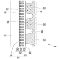
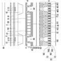
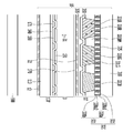
도 2는 일 실시예에 따른 색변환 패널의 단면도이다.
도 3은 일 실시예에 따른 색변환 패널의 단면도이다.
도 4는 일 실시예에 따른 색변환 패널의 단면도이다.
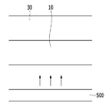
도 5는 일 실시예에 따른 표시 장치의 개략적인 단면도이다.
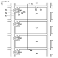
도 6은 일 실시예에 따른 표시 장치의 평면도이다.
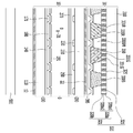
도 7은 도 6의 VII-VII선을 따라 자른 단면도이다.
도 8은 일 실시예에 따른 표시 장치의 평면도이다.
도 9은 도 8의 IX-IX선을 따라 자른 단면도이다.
도 10은 일 실시예에 따른 표시 장치의 단면도이다.
도 11 및 도 12는 일 실시예 및 비교예에 따른 투과도 및 반사도에 대한 그래프이다.
320: 편광층
330R, 330G: 색변환층
330B: 투과층
Claims (20)
- 기판,
상기 기판 위에 위치하며 소정의 간격으로 이격된 복수의 편광 패턴을 포함하는 편광층, 및
상기 편광층 위에 위치하며 양자점을 포함하는 색변환층 및 투과층,
을 포함하고,
상기 복수의 편광 패턴 중 적어도 하나는,
상기 기판 위에 위치하는 외광 간섭층, 및
상기 외광 간섭층 위에 위치하는 반사층을 포함하는 색변환 패널. - 제1항에서,
상기 복수의 편광 패턴 중 어느 하나의 너비(w)와, 서로 인접한 편광 패턴 사이의 간격(d)의 합(p=w+d)은 200 nm 이하인 색변환 패널. - 제1항에서,
상기 외광 간섭층은,
상기 기판 위에 위치하는 제1 금속층, 및
상기 제1 금속층 위에 위치하는 제1 무기층을 포함하는 색변환 패널. - 제3항에서,
상기 제1 금속층과 상기 기판 사이에 위치하는 제2 무기층을 더 포함하는 색변환 패널. - 제4항에서,
상기 제1 무기층 및 상기 제2 무기층은 금속산화물, 산화규소 및 질화규소 중 적어도 하나를 포함하는 색변환 패널. - 제3항에서,
상기 제1 금속층은 Cr, Mo 및 Ti 중 적어도 하나를 포함하는 색변환 패널. - 제1항에서,
상기 반사층은 금속 물질을 포함하는 색변환 패널. - 제1항에서,
상기 금속 물질은 Ag, Au, Cu, 및 Al으로 이루어진 군으로부터 선택된 적어도 하나를 포함하는 색변환 패널. - 제2항에서,
상기 복수의 편광 패턴 사이에 위치하는 광학층을 더 포함하는 색변환 패널. - 제9항에서,
상기 광학층의 굴절률은 1.0 내지 1.4인 색변환 패널. - 제1항에서,
상기 편광층은 상기 색변환층 및 상기 투과층과 맞닿는 색변환 패널. - 제1항에서,
상기 색변환층 및 상기 투과층 위에 위치하는 캡핑층을 더 포함하는 색변환 패널. - 표시 패널, 및
상기 표시 패널 위에 위치하는 색변환 패널을 포함하고,
상기 색변환 패널은,
기판,
상기 기판과 상기 표시 패널 사이에 위치하며 소정의 간격으로 이격된 복수의 편광 패턴을 포함하는 편광층, 및
상기 편광층과 상기 표시 패널 사이에 위치하며 양자점을 포함하는 색변환층 및 투과층을 포함하고,
상기 복수의 편광 패턴 중 적어도 하나는,
상기 기판과 상기 표시 패널 사이에 위치하는 외광 간섭층, 및
상기 외광 간섭층과 상기 표시 패널 사이에 위치하는 반사층을 포함하는 표시 장치. - 제13항에서,
상기 복수의 편광 패턴 중 어느 하나의 너비(w)와, 서로 인접한 편광 패턴 사이의 간격(d)의 합(p=w+d)은 200 nm 이하인 표시 장치. - 제13항에서,
상기 외광 간섭층은,
상기 기판과 상기 표시 패널 사이에 위치하는 제1 금속층, 및
상기 제1 금속층과 상기 표시 패널 사이에 위치하는 제1 무기층을 포함하는 표시 장치. - 제13항에서,
상기 복수의 편광 패턴 사이에 위치하는 광학층을 더 포함하는 표시 장치. - 제16항에서,
상기 광학층의 굴절률은 1.0 내지 1.4인 표시 장치. - 하부 표시판,
상기 하부 표시판과 중첩하는 색변환 패널, 및
상기 하부 표시판과 상기 색변환 패널 사이에 위치하는 액정층을 포함하고,
상기 색변환 패널은,
기판,
상기 기판과 상기 액정층 사이에 위치하며 소정의 간격으로 이격된 복수의 편광 패턴을 포함하는 편광층, 및
상기 편광층과 상기 액정층 사이에 위치하며 양자점을 포함하는 색변환층 및 투과층을 포함하고,
상기 복수의 편광 패턴 중 적어도 하나는,
상기 기판과 상기 액정층 사이에 위치하는 외광 간섭층, 및
상기 외광 간섭층과 상기 액정층 사이에 위치하는 반사층을 포함하는 표시 장치. - 제18항에서,
상기 복수의 편광 패턴 중 어느 하나의 너비(w)와, 서로 인접한 편광 패턴 사이의 간격(d)의 합(p=w+d)은 200 nm 이하인 표시 장치. - 제18항에서,
상기 복수의 편광 패턴 사이에 위치하는 광학층을 더 포함하고, 상기 광학층의 굴절률은 1.0 내지 1.4인 표시 장치.
Priority Applications (3)
| Application Number | Priority Date | Filing Date | Title |
|---|---|---|---|
| KR1020160067303A KR20170136109A (ko) | 2016-05-31 | 2016-05-31 | 색변환 패널 및 이를 포함하는 표시 장치 |
| US15/494,156 US10330974B2 (en) | 2016-05-31 | 2017-04-21 | Color conversion panel and display device including the same |
| CN201710397471.4A CN107450220A (zh) | 2016-05-31 | 2017-05-31 | 颜色转换面板以及包括该颜色转换面板的显示装置 |
Applications Claiming Priority (1)
| Application Number | Priority Date | Filing Date | Title |
|---|---|---|---|
| KR1020160067303A KR20170136109A (ko) | 2016-05-31 | 2016-05-31 | 색변환 패널 및 이를 포함하는 표시 장치 |
Publications (1)
| Publication Number | Publication Date |
|---|---|
| KR20170136109A true KR20170136109A (ko) | 2017-12-11 |
Family
ID=60418723
Family Applications (1)
| Application Number | Title | Priority Date | Filing Date |
|---|---|---|---|
| KR1020160067303A Ceased KR20170136109A (ko) | 2016-05-31 | 2016-05-31 | 색변환 패널 및 이를 포함하는 표시 장치 |
Country Status (3)
| Country | Link |
|---|---|
| US (1) | US10330974B2 (ko) |
| KR (1) | KR20170136109A (ko) |
| CN (1) | CN107450220A (ko) |
Cited By (3)
| Publication number | Priority date | Publication date | Assignee | Title |
|---|---|---|---|---|
| KR20190111177A (ko) * | 2018-03-21 | 2019-10-02 | 삼성디스플레이 주식회사 | 표시장치 |
| KR20200006206A (ko) * | 2018-07-09 | 2020-01-20 | 삼성디스플레이 주식회사 | 표시장치 |
| US10978518B2 (en) | 2019-01-03 | 2021-04-13 | Samsung Display Co., Ltd. | Display panel |
Families Citing this family (11)
| Publication number | Priority date | Publication date | Assignee | Title |
|---|---|---|---|---|
| CN108089384A (zh) * | 2016-11-21 | 2018-05-29 | 群创光电股份有限公司 | 显示装置 |
| KR102533686B1 (ko) * | 2018-01-18 | 2023-05-17 | 삼성디스플레이 주식회사 | 표시 장치 및 그 제조 방법 |
| CN108257949B (zh) * | 2018-01-24 | 2020-02-07 | 福州大学 | 可实现光效提取和色彩转换微米级led显示装置及制造方法 |
| CN110299383B (zh) * | 2018-03-21 | 2024-01-19 | 三星显示有限公司 | 显示设备 |
| US10762806B2 (en) * | 2018-04-24 | 2020-09-01 | Innolux Corporation | Display device |
| US20200012146A1 (en) * | 2018-07-05 | 2020-01-09 | Innolux Corporation | Electronic device |
| KR102772272B1 (ko) * | 2019-01-07 | 2025-02-24 | 삼성디스플레이 주식회사 | 표시 장치 |
| US11049884B2 (en) * | 2019-04-28 | 2021-06-29 | Wuhan China Star Optoelectronics Semiconductor Display Technology Co., Ltd. | Display panel and method of manufacturing same, and display module |
| KR20210142031A (ko) * | 2020-05-14 | 2021-11-24 | 삼성디스플레이 주식회사 | 표시 장치 |
| TW202247128A (zh) * | 2021-05-17 | 2022-12-01 | 美商元平台技術有限公司 | 具有偏極化發光增強的色彩轉換顯示器 |
| US12274125B2 (en) | 2021-05-17 | 2025-04-08 | Meta Platforms Technologies, Llc | Color conversion display with polarized emission enhancement |
Family Cites Families (30)
| Publication number | Priority date | Publication date | Assignee | Title |
|---|---|---|---|---|
| CN1242292C (zh) * | 2003-01-13 | 2006-02-15 | 元太科技工业股份有限公司 | 光干涉式彩色显示面板及光干涉调节元件 |
| CN1266525C (zh) * | 2003-03-26 | 2006-07-26 | 鸿富锦精密工业(深圳)有限公司 | 黑色矩阵、彩色滤光片和液晶显示装置 |
| KR20070010472A (ko) * | 2005-07-19 | 2007-01-24 | 삼성전자주식회사 | 하이브리드형 편광자와, 이의 제조 방법 및 이를 갖는표시장치 |
| KR20080020312A (ko) * | 2006-08-31 | 2008-03-05 | 삼성전자주식회사 | 자발광 액정 표시 장치 |
| US7957062B2 (en) * | 2007-02-06 | 2011-06-07 | Sony Corporation | Polarizing element and liquid crystal projector |
| KR100829756B1 (ko) * | 2007-03-02 | 2008-05-16 | 삼성에스디아이 주식회사 | 편광자 및 그를 포함하는 유기 발광 표시 장치 |
| WO2009066206A1 (en) | 2007-11-19 | 2009-05-28 | Koninklijke Philips Electronics N.V. | Light source and illumination system having a predefined external appearance |
| KR20100111103A (ko) | 2009-04-06 | 2010-10-14 | 삼성전자주식회사 | 액정 표시 장치 |
| US8294848B2 (en) * | 2008-10-01 | 2012-10-23 | Samsung Display Co., Ltd. | Liquid crystal display having light diffusion layer |
| JP5682437B2 (ja) * | 2010-09-07 | 2015-03-11 | ソニー株式会社 | 固体撮像素子、固体撮像装置、撮像機器、及び、偏光素子の製造方法 |
| JP5682312B2 (ja) * | 2011-01-05 | 2015-03-11 | ソニー株式会社 | 固体撮像装置の製造方法 |
| KR101177480B1 (ko) * | 2011-02-14 | 2012-08-24 | 엘지전자 주식회사 | 조명 장치 및 이를 포함하는 디스플레이 장치 |
| US8964012B2 (en) * | 2011-02-14 | 2015-02-24 | Samsung Electronics Co., Ltd. | Display panel having a polarizing layer and display apparatus having the same |
| JP2013104888A (ja) * | 2011-11-10 | 2013-05-30 | Sharp Corp | 表示装置 |
| JP2013167823A (ja) * | 2012-02-16 | 2013-08-29 | Dexerials Corp | 無機偏光板 |
| KR101977061B1 (ko) | 2012-07-10 | 2019-05-13 | 삼성디스플레이 주식회사 | 편광 소자, 이를 포함하는 표시 패널 및 이의 제조 방법 |
| KR20140074495A (ko) * | 2012-12-10 | 2014-06-18 | 삼성디스플레이 주식회사 | 포토루미네선트 패널, 이를 갖는 포토루미네선트 액정표시장치 및 이의 제조방법 |
| US9599869B2 (en) * | 2013-01-23 | 2017-03-21 | Samsung Display Co., Ltd. | Display apparatus |
| KR102117600B1 (ko) | 2013-05-28 | 2020-06-02 | 삼성디스플레이 주식회사 | 편광판 및 이를 포함하는 액정 표시 장치 |
| CN103399367B (zh) * | 2013-07-30 | 2016-02-17 | 合肥京东方光电科技有限公司 | 一种显示基板及其制造方法、显示装置 |
| KR102089661B1 (ko) * | 2013-08-27 | 2020-03-17 | 삼성전자주식회사 | 와이어 그리드 편광판 및 이를 구비하는 액정 표시패널 및 액정 표시장치 |
| KR102150859B1 (ko) * | 2014-01-13 | 2020-09-03 | 삼성디스플레이 주식회사 | 표시장치 |
| KR102119680B1 (ko) | 2014-02-11 | 2020-06-09 | 삼성디스플레이 주식회사 | 표시 장치 및 이의 구동 방법 |
| KR102239112B1 (ko) * | 2014-07-30 | 2021-04-13 | 삼성디스플레이 주식회사 | 표시장치 |
| KR20160028580A (ko) * | 2014-09-03 | 2016-03-14 | 삼성디스플레이 주식회사 | 컬러 변환층을 포함하는 표시장치 |
| CN104330915B (zh) * | 2014-11-07 | 2017-06-06 | 京东方科技集团股份有限公司 | 一种阵列基板、液晶显示面板及显示装置 |
| KR102243483B1 (ko) * | 2014-11-11 | 2021-04-22 | 삼성디스플레이 주식회사 | 표시 장치 |
| KR102305200B1 (ko) * | 2014-12-05 | 2021-09-27 | 삼성디스플레이 주식회사 | 와이어 그리드 편광자, 이를 포함하는 표시 장치 및 이의 제조방법 |
| CN105182594B (zh) * | 2015-08-25 | 2018-07-31 | 京东方科技集团股份有限公司 | 显示基板 |
| CN105204216A (zh) * | 2015-10-29 | 2015-12-30 | 深圳市华星光电技术有限公司 | Pdlc显示面板及其制作方法与液晶显示装置 |
-
2016
- 2016-05-31 KR KR1020160067303A patent/KR20170136109A/ko not_active Ceased
-
2017
- 2017-04-21 US US15/494,156 patent/US10330974B2/en active Active
- 2017-05-31 CN CN201710397471.4A patent/CN107450220A/zh active Pending
Cited By (3)
| Publication number | Priority date | Publication date | Assignee | Title |
|---|---|---|---|---|
| KR20190111177A (ko) * | 2018-03-21 | 2019-10-02 | 삼성디스플레이 주식회사 | 표시장치 |
| KR20200006206A (ko) * | 2018-07-09 | 2020-01-20 | 삼성디스플레이 주식회사 | 표시장치 |
| US10978518B2 (en) | 2019-01-03 | 2021-04-13 | Samsung Display Co., Ltd. | Display panel |
Also Published As
| Publication number | Publication date |
|---|---|
| US20170343853A1 (en) | 2017-11-30 |
| US10330974B2 (en) | 2019-06-25 |
| CN107450220A (zh) | 2017-12-08 |
Similar Documents
| Publication | Publication Date | Title |
|---|---|---|
| KR102765118B1 (ko) | 표시 장치 | |
| US11187942B2 (en) | Color conversion panel and display device including the same | |
| KR102618811B1 (ko) | 색변환 패널 및 이를 포함하는 표시 장치 | |
| KR102527215B1 (ko) | 색변환 패널 및 이를 포함하는 표시 장치 | |
| TWI737791B (zh) | 彩色濾光片、其製造方法,以及包含其的顯示設備 | |
| US9989806B2 (en) | Color conversion panel and display device including the same | |
| KR102770511B1 (ko) | 색변환 패널, 이의 제조 방법 및 이를 포함하는 표시 장치 | |
| KR102416572B1 (ko) | 표시 장치 | |
| US10330974B2 (en) | Color conversion panel and display device including the same | |
| KR102749824B1 (ko) | 색변환 패널 및 이를 포함하는 표시 장치 | |
| KR102584304B1 (ko) | 색변환 패널 및 이를 포함하는 표시 장치 | |
| KR20180085849A (ko) | 색변환 표시판 및 이를 포함하는 표시 장치 | |
| KR102555322B1 (ko) | 색변환 패널 및 이를 포함하는 표시 장치 | |
| US20180314107A1 (en) | Color conversion panel and display device including the same | |
| KR20170062595A (ko) | 색변환 패널, 이의 제조 방법 및 이를 포함하는 표시 장치 | |
| KR20190007130A (ko) | 표시 장치 | |
| KR102626391B1 (ko) | 표시 장치 | |
| KR20180056443A (ko) | 표시 장치 | |
| KR20180133979A (ko) | 표시 장치 | |
| US10707276B2 (en) | Display device | |
| CN108254966B (zh) | 颜色转换显示面板及包括颜色转换显示面板的显示设备 | |
| KR20190021516A (ko) | 색변환 표시판 및 이를 포함하는 표시 장치 | |
| KR20190067954A (ko) | 표시 장치 | |
| KR20180076422A (ko) | 색 변환 패널 및 이를 포함하는 표시 장치 |
Legal Events
| Date | Code | Title | Description |
|---|---|---|---|
| PA0109 | Patent application |
Patent event code: PA01091R01D Comment text: Patent Application Patent event date: 20160531 |
|
| PG1501 | Laying open of application | ||
| A201 | Request for examination | ||
| PA0201 | Request for examination |
Patent event code: PA02012R01D Patent event date: 20201217 Comment text: Request for Examination of Application Patent event code: PA02011R01I Patent event date: 20160531 Comment text: Patent Application |
|
| E902 | Notification of reason for refusal | ||
| PE0902 | Notice of grounds for rejection |
Comment text: Notification of reason for refusal Patent event date: 20220217 Patent event code: PE09021S01D |
|
| E601 | Decision to refuse application | ||
| PE0601 | Decision on rejection of patent |
Patent event date: 20220527 Comment text: Decision to Refuse Application Patent event code: PE06012S01D Patent event date: 20220217 Comment text: Notification of reason for refusal Patent event code: PE06011S01I |