KR20170139491A - 트랜시버 자기-간섭 제거기를 위한 회로 및 방법 - Google Patents
트랜시버 자기-간섭 제거기를 위한 회로 및 방법 Download PDFInfo
- Publication number
- KR20170139491A KR20170139491A KR1020177011681A KR20177011681A KR20170139491A KR 20170139491 A KR20170139491 A KR 20170139491A KR 1020177011681 A KR1020177011681 A KR 1020177011681A KR 20177011681 A KR20177011681 A KR 20177011681A KR 20170139491 A KR20170139491 A KR 20170139491A
- Authority
- KR
- South Korea
- Prior art keywords
- variable
- switches
- circuit
- local oscillator
- coupled
- Prior art date
- Legal status (The legal status is an assumption and is not a legal conclusion. Google has not performed a legal analysis and makes no representation as to the accuracy of the status listed.)
- Granted
Links
Images


Classifications
-
- H—ELECTRICITY
- H03—ELECTRONIC CIRCUITRY
- H03H—IMPEDANCE NETWORKS, e.g. RESONANT CIRCUITS; RESONATORS
- H03H11/00—Networks using active elements
-
- H—ELECTRICITY
- H03—ELECTRONIC CIRCUITRY
- H03H—IMPEDANCE NETWORKS, e.g. RESONANT CIRCUITS; RESONATORS
- H03H19/00—Networks using time-varying elements, e.g. N-path filters
- H03H19/002—N-path filters
-
- H—ELECTRICITY
- H03—ELECTRONIC CIRCUITRY
- H03H—IMPEDANCE NETWORKS, e.g. RESONANT CIRCUITS; RESONATORS
- H03H11/00—Networks using active elements
- H03H11/02—Multiple-port networks
- H03H11/04—Frequency selective two-port networks
- H03H11/0422—Frequency selective two-port networks using transconductance amplifiers, e.g. gmC filters
-
- H—ELECTRICITY
- H03—ELECTRONIC CIRCUITRY
- H03H—IMPEDANCE NETWORKS, e.g. RESONANT CIRCUITS; RESONATORS
- H03H7/00—Multiple-port networks comprising only passive electrical elements as network components
- H03H7/01—Frequency selective two-port networks
- H03H7/12—Bandpass or bandstop filters with adjustable bandwidth and fixed centre frequency
-
- H—ELECTRICITY
- H04—ELECTRIC COMMUNICATION TECHNIQUE
- H04B—TRANSMISSION
- H04B1/00—Details of transmission systems, not covered by a single one of groups H04B3/00 - H04B13/00; Details of transmission systems not characterised by the medium used for transmission
- H04B1/38—Transceivers, i.e. devices in which transmitter and receiver form a structural unit and in which at least one part is used for functions of transmitting and receiving
- H04B1/40—Circuits
- H04B1/50—Circuits using different frequencies for the two directions of communication
- H04B1/52—Hybrid arrangements, i.e. arrangements for transition from single-path two-direction transmission to single-direction transmission on each of two paths or vice versa
- H04B1/525—Hybrid arrangements, i.e. arrangements for transition from single-path two-direction transmission to single-direction transmission on each of two paths or vice versa with means for reducing leakage of transmitter signal into the receiver
-
- H—ELECTRICITY
- H04—ELECTRIC COMMUNICATION TECHNIQUE
- H04B—TRANSMISSION
- H04B17/00—Monitoring; Testing
- H04B17/30—Monitoring; Testing of propagation channels
- H04B17/309—Measuring or estimating channel quality parameters
- H04B17/336—Signal-to-interference ratio [SIR] or carrier-to-interference ratio [CIR]
-
- H—ELECTRICITY
- H04—ELECTRIC COMMUNICATION TECHNIQUE
- H04L—TRANSMISSION OF DIGITAL INFORMATION, e.g. TELEGRAPHIC COMMUNICATION
- H04L25/00—Baseband systems
- H04L25/02—Details ; arrangements for supplying electrical power along data transmission lines
- H04L25/03—Shaping networks in transmitter or receiver, e.g. adaptive shaping networks
- H04L25/03006—Arrangements for removing intersymbol interference
-
- H—ELECTRICITY
- H03—ELECTRONIC CIRCUITRY
- H03H—IMPEDANCE NETWORKS, e.g. RESONANT CIRCUITS; RESONATORS
- H03H11/00—Networks using active elements
- H03H11/02—Multiple-port networks
- H03H11/04—Frequency selective two-port networks
- H03H11/0422—Frequency selective two-port networks using transconductance amplifiers, e.g. gmC filters
- H03H11/0444—Simulation of ladder networks
-
- H—ELECTRICITY
- H03—ELECTRONIC CIRCUITRY
- H03H—IMPEDANCE NETWORKS, e.g. RESONANT CIRCUITS; RESONATORS
- H03H11/00—Networks using active elements
- H03H11/02—Multiple-port networks
- H03H11/36—Networks for connecting several sources or loads, working on the same frequency band, to a common load or source
- H03H11/362—Networks for connecting several sources or loads, working on the same frequency band, to a common load or source particularly adapted for use in common antenna systems
-
- H—ELECTRICITY
- H03—ELECTRONIC CIRCUITRY
- H03H—IMPEDANCE NETWORKS, e.g. RESONANT CIRCUITS; RESONATORS
- H03H2210/00—Indexing scheme relating to details of tunable filters
- H03H2210/01—Tuned parameter of filter characteristics
- H03H2210/012—Centre frequency; Cut-off frequency
-
- H—ELECTRICITY
- H03—ELECTRONIC CIRCUITRY
- H03H—IMPEDANCE NETWORKS, e.g. RESONANT CIRCUITS; RESONATORS
- H03H2210/00—Indexing scheme relating to details of tunable filters
- H03H2210/01—Tuned parameter of filter characteristics
- H03H2210/015—Quality factor or bandwidth
-
- H—ELECTRICITY
- H03—ELECTRONIC CIRCUITRY
- H03H—IMPEDANCE NETWORKS, e.g. RESONANT CIRCUITS; RESONATORS
- H03H2210/00—Indexing scheme relating to details of tunable filters
- H03H2210/01—Tuned parameter of filter characteristics
- H03H2210/017—Amplitude, gain or attenuation
-
- H—ELECTRICITY
- H03—ELECTRONIC CIRCUITRY
- H03H—IMPEDANCE NETWORKS, e.g. RESONANT CIRCUITS; RESONATORS
- H03H2210/00—Indexing scheme relating to details of tunable filters
- H03H2210/02—Variable filter component
- H03H2210/021—Amplifier, e.g. transconductance amplifier
-
- H—ELECTRICITY
- H03—ELECTRONIC CIRCUITRY
- H03H—IMPEDANCE NETWORKS, e.g. RESONANT CIRCUITS; RESONATORS
- H03H2210/00—Indexing scheme relating to details of tunable filters
- H03H2210/02—Variable filter component
- H03H2210/025—Capacitor
-
- H—ELECTRICITY
- H03—ELECTRONIC CIRCUITRY
- H03H—IMPEDANCE NETWORKS, e.g. RESONANT CIRCUITS; RESONATORS
- H03H2210/00—Indexing scheme relating to details of tunable filters
- H03H2210/02—Variable filter component
- H03H2210/028—Resistor
-
- H—ELECTRICITY
- H04—ELECTRIC COMMUNICATION TECHNIQUE
- H04B—TRANSMISSION
- H04B17/00—Monitoring; Testing
- H04B17/10—Monitoring; Testing of transmitters
- H04B17/101—Monitoring; Testing of transmitters for measurement of specific parameters of the transmitter or components thereof
- H04B17/104—Monitoring; Testing of transmitters for measurement of specific parameters of the transmitter or components thereof of other parameters, e.g. DC offset, delay or propagation times
Landscapes
- Engineering & Computer Science (AREA)
- Computer Networks & Wireless Communication (AREA)
- Signal Processing (AREA)
- Power Engineering (AREA)
- Quality & Reliability (AREA)
- Physics & Mathematics (AREA)
- Electromagnetism (AREA)
- Noise Elimination (AREA)
- Transceivers (AREA)
Abstract
Description
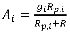
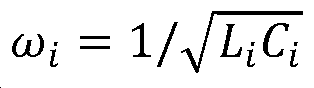
도 2는 일부 실시예들에 따른 2차 RLC 대역통과 필터의 모델의 예의 개략도이다.
도 3은 일부 실시예들에 따른 2차 Gm-C 대역통과 필터의 예의 개략도이다.
도 4는 일부 실시예들에 따른 반시계 방향 구성의 2차 Gm-C 대역통과 필터의 예의 개략도이다.
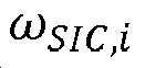
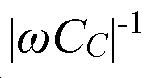
도 5는 일부 실시예들에 따른 필터 파라미터에 대한 변경이 필터 성능에 어떻게 영향을 미치는지를 나타내는 그래프들의 세트이다.
도 6은 일부 실시예들에 따른 2개의 자기-간섭 제거기를 포함하는 수신기의 예의 개략도이다.
도 7은 일부 실시예들에 따른 트랜스컨덕터 Gm 뱅크의 예의 개략도이다.
도 8은 일부 실시예들에 따른 국부 발진기 생성기의 예의 개략도이다.
도 9는 일부 실시예들에 따른 캘리브레이션 프로세스의 예의 흐름도이다.









Claims (10)
- 트랜시버 자기-간섭 제거기(transceiver self-interference canceller)를 위한 회로에 있어서,
각각이 상이한 서브-주파수 대역들에서의 안테나 격리도(antenna isolation)의 크기, 위상, 크기 기울기 및 위상 기울기 응답을 에뮬레이트(emulate)하는 복수의 RF 하이-Q 대역통과 필터를 포함하는, 트랜시버 자기-간섭 제거기를 위한 회로. - 제1항에 있어서, 상기 복수의 RF 하이-Q 대역통과 필터 각각은,
제어 입력, 송신기 신호에 결합된 제1 측, 및 제2 측을 갖는 제1 가변 저항;
각각이 제어 입력, 상기 가변 저항기의 제2 측에 결합된 제1 측, 및 제2 측을 갖는, 복수의 제1 스위치;
각각이 제어 입력, 접지에 연결된 제1 측, 및 상기 복수의 제1 스위치의 제2 측들 중 고유한 하나에 연결된 제2 측을 갖는, 복수의 제1 가변 커패시턴스;
각각이 제어 입력, 상기 복수의 제1 가변 커패시턴스의 제2 측들 중 고유한 하나에 결합된 제1 측, 및 제2 측을 갖는 복수의 제2 스위치;
제어 입력, 접지에 연결된 제1 측, 및 상기 복수의 제2 스위치의 제2 측들 각각에 결합된 제2 측을 갖는 제2 가변 저항;
제어 입력, 상기 복수의 제2 스위치의 제2 측들 각각에 연결된 제1 측, 및 수신기 신호에 결합된 제2 측을 갖는 제2 가변 커패시턴스;
각각이 상기 복수의 제1 가변 커패시턴스의 제2 측들 중 고유한 하나에 연결된 입력, 및 상기 복수의 제1 가변 커패시턴스의 제2 측들 중 고유한 하나에 연결된 출력을 갖는, 복수의 가변 트랜스컨덕터 - 상기 복수의 가변 트랜스컨덕터 각각에 대해, 상기 가변 트랜스컨덕터의 입력은 상기 가변 트랜스컨덕터의 출력에 연결되지 않음 -;
각각이 상기 복수의 제1 스위치의 제어 입력들 중 고유한 하나에 연결된 복수의 출력을 갖는 제1 국부 발진기 - 상기 제1 국부 발진기는 한 번에 상기 복수의 제1 스위치 중 하나를 턴 온함 -; 및
각각이 상기 복수의 제2 스위치의 제어 입력들 중 고유한 하나에 연결된 복수의 출력을 갖는 제2 국부 발진기
를 포함하고, 상기 제2 국부 발진기는 한 번에 상기 복수의 제2 스위치 중 하나를 턴 온하고, 상기 제2 국부 발진기의 복수의 출력은 상기 제1 국부 발진기의 복수의 출력으로부터 시간 시프트량만큼 시간적으로 시프트되는, 트랜시버 자기-간섭 제거기를 위한 회로. - 제2항에 있어서, 상기 제1 가변 저항은 복수의 스위치드 저항기(switched resistor)를 포함하는, 트랜시버 자기-간섭 제거기를 위한 회로.
- 제2항에 있어서, 상기 복수의 제1 가변 커패시턴스는 각각 복수의 스위치드 커패시터를 포함하는, 트랜시버 자기-간섭 제거기를 위한 회로.
- 제2항에 있어서, 상기 복수의 제2 스위치는 각각 트랜지스터인, 트랜시버 자기-간섭 제거기를 위한 회로.
- 제2항에 있어서, 상기 제2 가변 저항은 복수의 스위치드 저항기를 포함하는, 트랜시버 자기-간섭 제거기를 위한 회로.
- 제2항에 있어서, 상기 제2 가변 커패시턴스는 복수의 스위치드 커패시터를 포함하는, 트랜시버 자기-간섭 제거기를 위한 회로.
- 제2항에 있어서, 상기 복수의 가변 트랜스컨덕터는 각각 스위치드 트랜스컨덕터들의 뱅크를 포함하는, 트랜시버 자기-간섭 제거기를 위한 회로.
- 제2항에 있어서, 상기 제1 국부 발진기 및 상기 제2 국부 발진기 각각은 25% 국부 발진기인, 트랜시버 자기-간섭 제거기를 위한 회로.
- 자기-간섭 제거기를 캘리브레이션하는 방법에 있어서,
제거기가 오프인 상태에서 HSI를 측정하는 단계;
상기 제거기가 온인 상태에서 HSIC를 측정하는 단계;
상기 HSI 및 상기 HSIC의 크기 및 기울기가 일치하는지를 결정하는 단계;
상기 HSI 및 상기 HSIC의 크기 및 기울기가 일치하지 않는다고 결정될 때, 상기 제거기에서의 상대 저항, 커패시턴스, 또는 트랜스컨덕턴스를 조정하는 단계;
HSIC의 위상 및 크기를 조정하는 단계; 및
그룹 지연을 계산하는 단계
를 포함하는, 자기-간섭 제거기를 캘리브레이션하는 방법.
Applications Claiming Priority (5)
| Application Number | Priority Date | Filing Date | Title |
|---|---|---|---|
| US201462058575P | 2014-10-01 | 2014-10-01 | |
| US62/058,575 | 2014-10-01 | ||
| US201562233215P | 2015-09-25 | 2015-09-25 | |
| US62/233,215 | 2015-09-25 | ||
| PCT/US2015/053614 WO2016054455A1 (en) | 2014-10-01 | 2015-10-01 | Circuits and methods for transceiver self-interference cancellers |
Publications (2)
| Publication Number | Publication Date |
|---|---|
| KR20170139491A true KR20170139491A (ko) | 2017-12-19 |
| KR102250210B1 KR102250210B1 (ko) | 2021-05-10 |
Family
ID=55631571
Family Applications (1)
| Application Number | Title | Priority Date | Filing Date |
|---|---|---|---|
| KR1020177011681A Active KR102250210B1 (ko) | 2014-10-01 | 2015-10-01 | 트랜시버 자기-간섭 제거기를 위한 회로 및 방법 |
Country Status (5)
| Country | Link |
|---|---|
| US (1) | US10277204B2 (ko) |
| EP (1) | EP3202043B1 (ko) |
| JP (1) | JP6728193B2 (ko) |
| KR (1) | KR102250210B1 (ko) |
| WO (1) | WO2016054455A1 (ko) |
Families Citing this family (2)
| Publication number | Priority date | Publication date | Assignee | Title |
|---|---|---|---|---|
| WO2017069300A1 (ko) * | 2015-10-21 | 2017-04-27 | 엘지전자 주식회사 | Fdr 방식을 지원하는 환경에서 자기간섭 제거를 위한 자기간섭 복제 신호를 제어하는 방법 및 이를 위한 장치 |
| EP4135207B1 (en) * | 2017-06-30 | 2025-04-30 | Transfert Plus | Energy efficient ultra-wideband impulse radio method |
Citations (4)
| Publication number | Priority date | Publication date | Assignee | Title |
|---|---|---|---|---|
| US5473332A (en) * | 1994-08-10 | 1995-12-05 | Mcdonnell Douglas Corporation | RFI suppression circuit and method |
| US6693971B1 (en) * | 2000-02-29 | 2004-02-17 | Bae Systems Information And Electronic Systems Integration Inc. | Wideband co-site interference reduction apparatus |
| US20110256857A1 (en) * | 2010-04-20 | 2011-10-20 | Intersil Americas Inc. | Systems and Methods for Improving Antenna Isolation Using Signal Cancellation |
| JP2011239401A (ja) * | 2010-05-10 | 2011-11-24 | Samsung Techwin Co Ltd | 位相ノイズが除去される送受信機 |
Family Cites Families (9)
| Publication number | Priority date | Publication date | Assignee | Title |
|---|---|---|---|---|
| US7096042B2 (en) * | 2003-01-21 | 2006-08-22 | Interdigital Technology Corporation | System and method for increasing cellular system capacity by the use of the same frequency and time slot for both uplink and downlink transmissions |
| WO2008030165A1 (en) | 2006-09-05 | 2008-03-13 | Buon Kiong Lau | Antenna system and method for operating an antenna system |
| WO2010019017A2 (ko) | 2008-08-14 | 2010-02-18 | 한국전자통신연구원 | Ofdm 기반 무선통신 시스템에서 동일 주파수 릴레이 및 리피터의 자기간섭 제거 방법 및 그 장치 |
| US8081946B2 (en) | 2008-12-23 | 2011-12-20 | L-3 Communications Integrated Systems L.P. | Interference cancellation for reconfigurable direct RF bandpass sampling interference cancellation |
| US8755756B1 (en) | 2009-04-29 | 2014-06-17 | Qualcomm Incorporated | Active cancellation of interference in a wireless communication system |
| US8149742B1 (en) * | 2009-06-26 | 2012-04-03 | Rockwell Collins, Inc. | System and method for receiving and transmitting signals |
| US8620242B2 (en) | 2010-08-19 | 2013-12-31 | Broadcom Corporation | High performance transmitter preamplification chain with calibration feedback |
| WO2013173252A1 (en) | 2012-05-13 | 2013-11-21 | Invention Mine Llc | Full duplex wireless transmission with channel phase-based encryption |
| US9203455B2 (en) | 2012-08-14 | 2015-12-01 | Broadcom Corporation | Full duplex system with self-interference cancellation |
-
2015
- 2015-10-01 EP EP15847787.7A patent/EP3202043B1/en active Active
- 2015-10-01 US US15/515,823 patent/US10277204B2/en active Active
- 2015-10-01 WO PCT/US2015/053614 patent/WO2016054455A1/en not_active Ceased
- 2015-10-01 KR KR1020177011681A patent/KR102250210B1/ko active Active
- 2015-10-01 JP JP2017538162A patent/JP6728193B2/ja active Active
Patent Citations (4)
| Publication number | Priority date | Publication date | Assignee | Title |
|---|---|---|---|---|
| US5473332A (en) * | 1994-08-10 | 1995-12-05 | Mcdonnell Douglas Corporation | RFI suppression circuit and method |
| US6693971B1 (en) * | 2000-02-29 | 2004-02-17 | Bae Systems Information And Electronic Systems Integration Inc. | Wideband co-site interference reduction apparatus |
| US20110256857A1 (en) * | 2010-04-20 | 2011-10-20 | Intersil Americas Inc. | Systems and Methods for Improving Antenna Isolation Using Signal Cancellation |
| JP2011239401A (ja) * | 2010-05-10 | 2011-11-24 | Samsung Techwin Co Ltd | 位相ノイズが除去される送受信機 |
Also Published As
| Publication number | Publication date |
|---|---|
| JP2017535217A (ja) | 2017-11-24 |
| EP3202043A4 (en) | 2018-10-24 |
| US10277204B2 (en) | 2019-04-30 |
| KR102250210B1 (ko) | 2021-05-10 |
| JP6728193B2 (ja) | 2020-07-22 |
| WO2016054455A1 (en) | 2016-04-07 |
| EP3202043A1 (en) | 2017-08-09 |
| US20170250677A1 (en) | 2017-08-31 |
| EP3202043B1 (en) | 2021-02-24 |
Similar Documents
| Publication | Publication Date | Title |
|---|---|---|
| Zhou et al. | Integrated wideband self-interference cancellation in the RF domain for FDD and full-duplex wireless | |
| Song et al. | RF filter synthesis based on passively coupled N-path resonators | |
| US8723619B2 (en) | Filter arrangement having first and second duplex filters | |
| CN103503314B (zh) | Mems可调陷波滤波器频率自动控制回路系统和方法 | |
| US9654983B2 (en) | Tunable filter employing feedforward cancellation | |
| Duipmans et al. | Analysis of the signal transfer and folding in N-path filters with a series inductance | |
| CN104821869B (zh) | 双工装置、无线设备和相关方法 | |
| JP6251414B2 (ja) | 調整可能なインピーダンスを提供するための回路及び方法 | |
| EP2923446B1 (en) | Transceiver front-end | |
| Nagulu et al. | A full-duplex receiver leveraging multiphase switched-capacitor-delay based multi-domain FIR filter cancelers | |
| US20190036217A1 (en) | Selectable Filtering with Switching | |
| Regev et al. | Analysis and design of quasi-circulating quadrature hybrid for full-duplex wireless | |
| KR102250210B1 (ko) | 트랜시버 자기-간섭 제거기를 위한 회로 및 방법 | |
| Tapen et al. | An integrated, software-defined FDD transceiver: Distributed duplexing theory and operation | |
| Garikapati et al. | Performance comparison of time-domain and frequency-domain RF self-interference cancellation in full-duplex wireless systems | |
| Ramakrishnan | Design of integrated full-duplex wireless transceivers | |
| CN110995293B (zh) | 带内波动抑制装置和射频系统 | |
| KR101449484B1 (ko) | 직접 변환 수신기 | |
| Dorn | An electrical balance duplexer architecture without inherent insertion loss limitation | |
| CN209375595U (zh) | 低通匹配式大动态常数相位的数控衰减电路 | |
| Yang | Switched inductor-capacitor CMOS circuits for radio frequency front-ends | |
| WO2024126746A1 (en) | Improved n-plexer | |
| Snygg et al. | True-Time Delay Cancellers for Full-Duplex | |
| Michetti et al. | A Modulation-Defined RF Micro-Acoustic Delay Line based on ScAlN MEMS Resonators for Self-Interference Cancellation | |
| Yuksel | Design and Theoretical Analysis of Wideband Tunable Duplexing Transceivers |
Legal Events
| Date | Code | Title | Description |
|---|---|---|---|
| PA0105 | International application |
Patent event date: 20170427 Patent event code: PA01051R01D Comment text: International Patent Application |
|
| N231 | Notification of change of applicant | ||
| PN2301 | Change of applicant |
Patent event date: 20171201 Comment text: Notification of Change of Applicant Patent event code: PN23011R01D |
|
| PG1501 | Laying open of application | ||
| A201 | Request for examination | ||
| A302 | Request for accelerated examination | ||
| PA0201 | Request for examination |
Patent event code: PA02012R01D Patent event date: 20200928 Comment text: Request for Examination of Application |
|
| PA0302 | Request for accelerated examination |
Patent event date: 20200928 Patent event code: PA03022R01D Comment text: Request for Accelerated Examination |
|
| E701 | Decision to grant or registration of patent right | ||
| PE0701 | Decision of registration |
Patent event code: PE07011S01D Comment text: Decision to Grant Registration Patent event date: 20210204 |
|
| GRNT | Written decision to grant | ||
| PR0701 | Registration of establishment |
Comment text: Registration of Establishment Patent event date: 20210503 Patent event code: PR07011E01D |
|
| PR1002 | Payment of registration fee |
Payment date: 20210503 End annual number: 3 Start annual number: 1 |
|
| PG1601 | Publication of registration | ||
| PR1001 | Payment of annual fee |
Payment date: 20250422 Start annual number: 5 End annual number: 5 |