KR20170141665A - 3차원 메모리를 위한 소켓 구조물 - Google Patents
3차원 메모리를 위한 소켓 구조물 Download PDFInfo
- Publication number
- KR20170141665A KR20170141665A KR1020177029491A KR20177029491A KR20170141665A KR 20170141665 A KR20170141665 A KR 20170141665A KR 1020177029491 A KR1020177029491 A KR 1020177029491A KR 20177029491 A KR20177029491 A KR 20177029491A KR 20170141665 A KR20170141665 A KR 20170141665A
- Authority
- KR
- South Korea
- Prior art keywords
- electrode
- edge
- planar
- electrodes
- horizontal
- Prior art date
- Legal status (The legal status is an assumption and is not a legal conclusion. Google has not performed a legal analysis and makes no representation as to the accuracy of the status listed.)
- Abandoned
Links
Images






Classifications
-
- H—ELECTRICITY
- H10—SEMICONDUCTOR DEVICES; ELECTRIC SOLID-STATE DEVICES NOT OTHERWISE PROVIDED FOR
- H10B—ELECTRONIC MEMORY DEVICES
- H10B41/00—Electrically erasable-and-programmable ROM [EEPROM] devices comprising floating gates
- H10B41/20—Electrically erasable-and-programmable ROM [EEPROM] devices comprising floating gates characterised by three-dimensional [3D] arrangements, e.g. with cells on different height levels
- H10B41/23—Electrically erasable-and-programmable ROM [EEPROM] devices comprising floating gates characterised by three-dimensional [3D] arrangements, e.g. with cells on different height levels with source and drain on different levels, e.g. with sloping channels
- H10B41/27—Electrically erasable-and-programmable ROM [EEPROM] devices comprising floating gates characterised by three-dimensional [3D] arrangements, e.g. with cells on different height levels with source and drain on different levels, e.g. with sloping channels the channels comprising vertical portions, e.g. U-shaped channels
-
- H01L27/11556—
-
- H01L21/768—
-
- H01L27/11524—
-
- H01L27/11548—
-
- H01L27/1157—
-
- H01L27/11575—
-
- H01L27/11582—
-
- H01L27/2481—
-
- H01L45/16—
-
- H—ELECTRICITY
- H10—SEMICONDUCTOR DEVICES; ELECTRIC SOLID-STATE DEVICES NOT OTHERWISE PROVIDED FOR
- H10B—ELECTRONIC MEMORY DEVICES
- H10B41/00—Electrically erasable-and-programmable ROM [EEPROM] devices comprising floating gates
- H10B41/30—Electrically erasable-and-programmable ROM [EEPROM] devices comprising floating gates characterised by the memory core region
- H10B41/35—Electrically erasable-and-programmable ROM [EEPROM] devices comprising floating gates characterised by the memory core region with a cell select transistor, e.g. NAND
-
- H—ELECTRICITY
- H10—SEMICONDUCTOR DEVICES; ELECTRIC SOLID-STATE DEVICES NOT OTHERWISE PROVIDED FOR
- H10B—ELECTRONIC MEMORY DEVICES
- H10B41/00—Electrically erasable-and-programmable ROM [EEPROM] devices comprising floating gates
- H10B41/50—Electrically erasable-and-programmable ROM [EEPROM] devices comprising floating gates characterised by the boundary region between the core region and the peripheral circuit region
-
- H—ELECTRICITY
- H10—SEMICONDUCTOR DEVICES; ELECTRIC SOLID-STATE DEVICES NOT OTHERWISE PROVIDED FOR
- H10B—ELECTRONIC MEMORY DEVICES
- H10B43/00—EEPROM devices comprising charge-trapping gate insulators
- H10B43/20—EEPROM devices comprising charge-trapping gate insulators characterised by three-dimensional [3D] arrangements, e.g. with cells on different height levels
- H10B43/23—EEPROM devices comprising charge-trapping gate insulators characterised by three-dimensional [3D] arrangements, e.g. with cells on different height levels with source and drain on different levels, e.g. with sloping channels
- H10B43/27—EEPROM devices comprising charge-trapping gate insulators characterised by three-dimensional [3D] arrangements, e.g. with cells on different height levels with source and drain on different levels, e.g. with sloping channels the channels comprising vertical portions, e.g. U-shaped channels
-
- H—ELECTRICITY
- H10—SEMICONDUCTOR DEVICES; ELECTRIC SOLID-STATE DEVICES NOT OTHERWISE PROVIDED FOR
- H10B—ELECTRONIC MEMORY DEVICES
- H10B43/00—EEPROM devices comprising charge-trapping gate insulators
- H10B43/30—EEPROM devices comprising charge-trapping gate insulators characterised by the memory core region
- H10B43/35—EEPROM devices comprising charge-trapping gate insulators characterised by the memory core region with cell select transistors, e.g. NAND
-
- H—ELECTRICITY
- H10—SEMICONDUCTOR DEVICES; ELECTRIC SOLID-STATE DEVICES NOT OTHERWISE PROVIDED FOR
- H10B—ELECTRONIC MEMORY DEVICES
- H10B43/00—EEPROM devices comprising charge-trapping gate insulators
- H10B43/50—EEPROM devices comprising charge-trapping gate insulators characterised by the boundary region between the core and peripheral circuit regions
-
- H—ELECTRICITY
- H10—SEMICONDUCTOR DEVICES; ELECTRIC SOLID-STATE DEVICES NOT OTHERWISE PROVIDED FOR
- H10B—ELECTRONIC MEMORY DEVICES
- H10B63/00—Resistance change memory devices, e.g. resistive RAM [ReRAM] devices
- H10B63/80—Arrangements comprising multiple bistable or multi-stable switching components of the same type on a plane parallel to the substrate, e.g. cross-point arrays
- H10B63/84—Arrangements comprising multiple bistable or multi-stable switching components of the same type on a plane parallel to the substrate, e.g. cross-point arrays arranged in a direction perpendicular to the substrate, e.g. 3D cell arrays
-
- H—ELECTRICITY
- H10—SEMICONDUCTOR DEVICES; ELECTRIC SOLID-STATE DEVICES NOT OTHERWISE PROVIDED FOR
- H10N—ELECTRIC SOLID-STATE DEVICES NOT OTHERWISE PROVIDED FOR
- H10N70/00—Solid-state devices having no potential barriers, and specially adapted for rectifying, amplifying, oscillating or switching
- H10N70/011—Manufacture or treatment of multistable switching devices
-
- H—ELECTRICITY
- H10—SEMICONDUCTOR DEVICES; ELECTRIC SOLID-STATE DEVICES NOT OTHERWISE PROVIDED FOR
- H10W—GENERIC PACKAGES, INTERCONNECTIONS, CONNECTORS OR OTHER CONSTRUCTIONAL DETAILS OF DEVICES COVERED BY CLASS H10
- H10W20/00—Interconnections in chips, wafers or substrates
- H10W20/01—Manufacture or treatment
-
- H—ELECTRICITY
- H10—SEMICONDUCTOR DEVICES; ELECTRIC SOLID-STATE DEVICES NOT OTHERWISE PROVIDED FOR
- H10W—GENERIC PACKAGES, INTERCONNECTIONS, CONNECTORS OR OTHER CONSTRUCTIONAL DETAILS OF DEVICES COVERED BY CLASS H10
- H10W20/00—Interconnections in chips, wafers or substrates
- H10W20/40—Interconnections external to wafers or substrates, e.g. back-end-of-line [BEOL] metallisations or vias connecting to gate electrodes
- H10W20/41—Interconnections external to wafers or substrates, e.g. back-end-of-line [BEOL] metallisations or vias connecting to gate electrodes characterised by their conductive parts
- H10W20/42—Vias, e.g. via plugs
Landscapes
- Engineering & Computer Science (AREA)
- Manufacturing & Machinery (AREA)
- Semiconductor Memories (AREA)
Abstract
Description
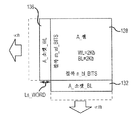
도 2는 3차원 메모리 구조물의 영역들을 평면도로 도시한다.
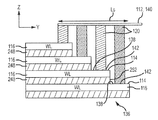
도 3은 종래 기술의 3차원 메모리 구조물을 입면도로 도시한다.
도 4는 도 3의 종래 기술의 3차원 메모리 구조물을 평면도로 도시한다.
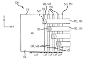
도 5는 본 개시내용의 실시예에 따른 3차원 메모리 구조물을 입면도로 도시한다.
도 6은 도 5의 3차원 메모리 구조물을 평면도로 도시한다.
도 7은 기준 3차원 메모리 구조물의 면적 효율과 비교하여 본 발명의 실시예에 따른 예시적인 3차원 메모리 구조물의 면적 효율을 나타내는 그래프이다.
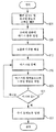
도 8은 본 개시내용의 실시예에 따른 방법의 양태를 도시하는 플로차트이다.
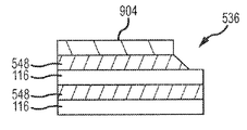
도 9a는 본 개시내용의 실시예에 따른 계단형 컨택트 구조물을 형성하기 위한 프로세스의 단계들을 도시한다.
도 9b는 본 개시내용의 실시예에 따른 계단형 컨택트 구조물을 형성하기 위한 프로세스의 단계들을 도시한다.
도 9c는 본 개시내용의 실시예에 따른 계단형 컨택트 구조물을 형성하기 위한 프로세스의 단계들을 도시한다.
도 9d는 본 개시내용의 실시예에 따른 계단형 컨택트 구조물을 형성하기 위한 프로세스의 단계들을 도시한다.

Claims (20)
- 3차원 메모리 구조물로서,
메모리 어레이 체적, ―상기 메모리 어레이 체적은, x, y, 및 z 차원으로 연장되고, 상기 메모리 어레이 체적은 복수의 메모리 셀을 포함함―;
소켓 영역, ―상기 소켓 영역은 상기 메모리 어레이 체적의 한 측면을 따라 위치하되, 상기 메모리 어레이 체적의 상기 한 측면을 따라 x 차원으로 연장되고, 상기 메모리 어레이 체적으로부터 y 차원으로 연장됨―;
x 및 y 차원으로 연장되는 평면들에 놓인 복수의 유전체 층; 및
x 및 y 차원으로 연장되는 평면들에 놓인 복수의 수평 전극
을 포함하고,
상기 복수의 수평 전극에 포함된 수평 전극들은 z 차원으로 적층되며,
상기 복수의 수평 전극에 포함된 인접한 수평 전극들은 상기 복수의 유전체 층에 포함된 유전체 층들 중 적어도 하나에 의해 z 차원에서 서로 분리되고,
적어도 제1 방향으로 상기 z 차원을 따라 이동함에 따라, 상기 수평 전극들은 상기 메모리 어레이 영역으로부터 제1 소켓 영역으로 더 많은 양만큼 연장되어 계단형 구조물을 형성하며,
제1 수평 전극과 제2 수평 전극 사이에 배치된 유전체 층의 엣지는, 상기 제1 수평 전극의 엣지와 상기 제2 수평 전극의 엣지 사이에 위치하며,
상기 제1 소켓 영역 내에서, 상기 복수의 수평 전극 중의 각각의 수평 전극은, 수평 전극들 각각이 z 차원에 평행한 하나 이상의 라인을 따라 액세스가능하도록, 유전체 층에 의해 덮이지 않은 부분을 포함하는, 3차원 메모리 구조물. - 제1항에 있어서,
복수의 접속 도체를 더 포함하고, 상기 접속 도체들 각각은 z 차원을 따라 연장되고, 상기 소켓 영역 내의 대응하는 수평 전극의 일부와 접촉하는, 3차원 메모리 구조물. - 제2항에 있어서, 상기 접속 도체들 각각은 상기 대응하는 수평 전극에 인접한 적어도 제1 유전체 층의 엣지의 일부와 접촉하는, 3차원 메모리 구조물.
- 제3항에 있어서, 상기 대응하는 수평 전극에 인접한 상기 적어도 제1 유전체 층의 엣지는 경사져 있는, 3차원 메모리 구조물.
- 제3항에 있어서, 상기 접속 도체들 중 적어도 일부는 상기 대응하는 수평 전극의 제1 측 상의 상기 유전체 층의 엣지의 일부 및 상기 대응하는 수평 전극의 제2 측 상의 상기 유전체 층의 엣지의 일부와 접촉하는, 3차원 메모리 구조물.
- 제5항에 있어서, 상기 접속 도체들 중 적어도 일부는 상기 대응하는 수평 전극의 엣지면 및 상단면의 일부와 접촉하는, 3차원 메모리 구조물.
- 제1항에 있어서, 상기 복수의 유전체 층 중의 각각의 유전체 층의 엣지 부분은 상기 엣지가 z 차원에 평행하지 않도록 경사져 있는, 3차원 메모리 구조물.
- 제7항에 있어서,
복수의 접속 도체를 더 포함하고, 상기 접속 도체들 각각은 대응하는 수평 전극의 상단면 및 엣지면과 접촉하는, 3차원 메모리 구조물. - 제8항에 있어서, 상기 접속 도체들 중 적어도 일부는 상기 유전체 층들 중 적어도 하나의 경사진 엣지와 접촉하는, 3차원 메모리 구조물.
- 소켓 영역으로서,
복수의 절연 층; 및
복수의 평면 전극을 포함하고,
인접한 평면 전극들은 상기 절연 층들 중 적어도 하나에 의해 서로 분리되며,
각각의 평면 전극은, 각각의 평면 전극의 일부가 계단을 형성하도록 상기 소켓 영역 내에서 상이한 거리로 연장되고;
각각의 절연 층의 단부면(end surface)의 적어도 일부는 인접한 평면 전극들의 단부면들 사이에 위치하는, 소켓 영역. - 제10항에 있어서, 상기 절연 층들 각각의 단부면은 경사져 있는, 소켓 영역.
- 제11항에 있어서,
복수의 접속 도체를 더 포함하고, 상기 복수의 접속 도체 중의 각각의 접속 도체는 상기 평면 전극들 중 하나에 접속되는, 소켓 영역. - 제12항에 있어서, 상기 접속 도체들 각각은 상기 절연 층들 중 적어도 하나와 접촉하는, 소켓 영역.
- 제13항에 있어서, 상기 접속 도체들 각각은 적어도 평면 전극의 엣지면에 접속되는, 소켓 영역.
- 제12항에 있어서, 상기 접속 도체들 중 적어도 하나는 상기 절연 층들 중 2개와 접촉하는, 소켓 영역.
- 제12항에 있어서, 상기 평면 전극들은 상기 소켓 영역으로부터 3차원 메모리 구조물로 연장되는, 소켓 영역.
- 계단형 컨택트 소켓 영역을 형성하기 위한 방법으로서,
복수의 평면 전극 및 복수의 절연 층을 포함하는 스택을 제공하는 단계, ―인접한 평면 전극들은 절연 층에 의해 서로 분리됨―;
상기 스택 상에 마스크를 배치하는 단계;
상기 마스크 아래에 있지 않은 상기 복수의 절연 층 중의 제1 절연 층의 제1 부분을 에칭하여 상기 복수의 평면 전극 중의 제1 평면 전극의 제1 부분을 노출시키는 단계;
마스크를 풀백(pull back)하는 단계; 및
상기 마스크를 풀백한 후에, 상기 마스크를 풀백함으로써 노출된 상기 제1 절연 층의 제2 부분을 에칭하고, 상기 제1 평면 전극의 상기 제1 부분의 일부를 에칭하고, 상기 복수의 절연 층에 포함된 제2 절연 층의 제1 부분을 에칭하는 단계, ― 상기 에칭에 의해 형성된 상기 제2 절연 층의 엣지는 경사져 있고 상기 제1 평면 전극의 엣지로부터 상기 제1 평면 전극의 엣지와 상기 제2 평면 전극의 엣지 사이로 연장됨―;
를 포함하는 방법. - 제17항에 있어서, 상기 제1 절연 층의 엣지는 경사져 있는, 방법.
- 제18항에 있어서, 상기 제1 및 제2 평면 전극들의 엣지들은 수직인, 방법.
- 제19항에 있어서,
복수의 접속 도체를 형성하는 단계를 더 포함하고, 각각의 접속 도체는 평면 전극들 중 하나의 상단면 및 엣지면에 전기적으로 접속되는, 방법.
Applications Claiming Priority (3)
| Application Number | Priority Date | Filing Date | Title |
|---|---|---|---|
| US14/695,835 | 2015-04-24 | ||
| US14/695,835 US9515125B2 (en) | 2015-04-24 | 2015-04-24 | Socket structure for three-dimensional memory |
| PCT/JP2016/002025 WO2016170759A1 (en) | 2015-04-24 | 2016-04-14 | Socket structure for three-dimensional memory |
Publications (1)
| Publication Number | Publication Date |
|---|---|
| KR20170141665A true KR20170141665A (ko) | 2017-12-26 |
Family
ID=55863153
Family Applications (1)
| Application Number | Title | Priority Date | Filing Date |
|---|---|---|---|
| KR1020177029491A Abandoned KR20170141665A (ko) | 2015-04-24 | 2016-04-14 | 3차원 메모리를 위한 소켓 구조물 |
Country Status (4)
| Country | Link |
|---|---|
| US (3) | US9515125B2 (ko) |
| JP (1) | JP6788607B2 (ko) |
| KR (1) | KR20170141665A (ko) |
| WO (1) | WO2016170759A1 (ko) |
Families Citing this family (8)
| Publication number | Priority date | Publication date | Assignee | Title |
|---|---|---|---|---|
| US9478556B2 (en) | 2014-09-11 | 2016-10-25 | Kabushiki Kaisha Toshiba | Semiconductor memory device |
| KR102536261B1 (ko) | 2015-12-18 | 2023-05-25 | 삼성전자주식회사 | 3차원 반도체 장치 |
| US9767901B1 (en) * | 2016-08-24 | 2017-09-19 | Hewlett Packard Enterprise Development Lp | Circuits having selector devices with different I-V responses |
| US10777566B2 (en) * | 2017-11-10 | 2020-09-15 | Macronix International Co., Ltd. | 3D array arranged for memory and in-memory sum-of-products operations |
| US10453854B2 (en) | 2017-11-15 | 2019-10-22 | Sandisk Technologies Llc | Three-dimensional memory device with thickened word lines in terrace region |
| CN111149206B (zh) * | 2017-11-15 | 2023-08-18 | 桑迪士克科技有限责任公司 | 在平台区中具有加厚字线的三维存储器器件及其制造方法 |
| US10461163B2 (en) | 2017-11-15 | 2019-10-29 | Sandisk Technologies Llc | Three-dimensional memory device with thickened word lines in terrace region and method of making thereof |
| US11222695B2 (en) * | 2019-11-15 | 2022-01-11 | Micron Technology, Inc. | Socket design for a memory device |
Family Cites Families (9)
| Publication number | Priority date | Publication date | Assignee | Title |
|---|---|---|---|---|
| ITTO20021118A1 (it) * | 2002-12-24 | 2004-06-25 | St Microelectronics Srl | Dispositivo mos e procedimento di fabbricazione di |
| JP5016832B2 (ja) * | 2006-03-27 | 2012-09-05 | 株式会社東芝 | 不揮発性半導体記憶装置及びその製造方法 |
| KR101065140B1 (ko) * | 2008-03-17 | 2011-09-16 | 가부시끼가이샤 도시바 | 반도체 기억 장치 |
| JP2010027870A (ja) * | 2008-07-18 | 2010-02-04 | Toshiba Corp | 半導体記憶装置及びその製造方法 |
| JP5380190B2 (ja) * | 2009-07-21 | 2014-01-08 | 株式会社東芝 | 不揮発性半導体記憶装置及びその製造方法 |
| KR101559958B1 (ko) * | 2009-12-18 | 2015-10-13 | 삼성전자주식회사 | 3차원 반도체 장치의 제조 방법 및 이에 따라 제조된 3차원 반도체 장치 |
| JP2011211039A (ja) * | 2010-03-30 | 2011-10-20 | Toshiba Corp | 記憶装置及びその製造方法 |
| US8885382B2 (en) * | 2012-06-29 | 2014-11-11 | Intel Corporation | Compact socket connection to cross-point array |
| JP2015056452A (ja) * | 2013-09-10 | 2015-03-23 | 株式会社東芝 | 半導体記憶装置及びその製造方法 |
-
2015
- 2015-04-24 US US14/695,835 patent/US9515125B2/en not_active Expired - Fee Related
-
2016
- 2016-04-14 KR KR1020177029491A patent/KR20170141665A/ko not_active Abandoned
- 2016-04-14 WO PCT/JP2016/002025 patent/WO2016170759A1/en not_active Ceased
- 2016-04-14 JP JP2017552102A patent/JP6788607B2/ja not_active Expired - Fee Related
- 2016-11-03 US US15/342,819 patent/US9728722B2/en not_active Expired - Fee Related
-
2017
- 2017-06-14 US US15/623,030 patent/US9935266B2/en active Active
Also Published As
| Publication number | Publication date |
|---|---|
| US20160315121A1 (en) | 2016-10-27 |
| US20170077399A1 (en) | 2017-03-16 |
| US9728722B2 (en) | 2017-08-08 |
| US9515125B2 (en) | 2016-12-06 |
| JP6788607B2 (ja) | 2020-11-25 |
| US20170288141A1 (en) | 2017-10-05 |
| WO2016170759A1 (en) | 2016-10-27 |
| JP2018513559A (ja) | 2018-05-24 |
| US9935266B2 (en) | 2018-04-03 |
Similar Documents
| Publication | Publication Date | Title |
|---|---|---|
| KR20170141665A (ko) | 3차원 메모리를 위한 소켓 구조물 | |
| JP2022510370A5 (ko) | ||
| US10050085B2 (en) | Block architecture for vertical memory array | |
| KR102024723B1 (ko) | 3차원 반도체 장치 | |
| US8835990B2 (en) | 3D memory array | |
| US8482133B2 (en) | Semiconductor package | |
| US8946892B2 (en) | Semiconductor package | |
| KR20210019226A (ko) | 적층 반도체 칩을 포함하는 반도체 패키지 | |
| WO2018119987A1 (en) | Dual in-line memory modules and connectors for increased system performance | |
| US9305901B2 (en) | Non-circular die package interconnect | |
| US8614507B2 (en) | Semiconductor devices having lower and upper interconnection structures that exhibit reduced coupling | |
| US20150155388A1 (en) | Semiconductor structure | |
| CN102881317B (zh) | 三维存储器阵列 | |
| US11271154B2 (en) | Magnetic tunnel junction (MTJ) device | |
| US20130168633A1 (en) | Semiconductor device and manufacturing method thereof | |
| US20170069567A1 (en) | Memory structure | |
| WO2020121491A1 (ja) | 半導体モジュール及びその製造方法 | |
| US20150349440A1 (en) | Semiconductor module socket and connection structure of the same | |
| US20160099209A1 (en) | Memory device and manufacturing method thereof | |
| US20250220930A1 (en) | Integrated circuits including polysilicon resistors | |
| US7492605B2 (en) | Power plane to reduce voltage difference between connector power pins | |
| US8542515B2 (en) | Connection and addressing of multi-plane crosspoint devices | |
| US12087716B2 (en) | Techniques for positioning bond pads of microelectronic devices and related microelectronic devices, methods, and systems | |
| US20250181812A1 (en) | Substrate design assisting device, substrate design assisting system, and data structure related to circuit information | |
| US20250210093A1 (en) | 3d dram with cmos-between-array architecture |
Legal Events
| Date | Code | Title | Description |
|---|---|---|---|
| PA0105 | International application |
St.27 status event code: A-0-1-A10-A15-nap-PA0105 |
|
| PG1501 | Laying open of application |
St.27 status event code: A-1-1-Q10-Q12-nap-PG1501 |
|
| PA0201 | Request for examination |
St.27 status event code: A-1-2-D10-D11-exm-PA0201 |
|
| D13-X000 | Search requested |
St.27 status event code: A-1-2-D10-D13-srh-X000 |
|
| D14-X000 | Search report completed |
St.27 status event code: A-1-2-D10-D14-srh-X000 |
|
| P22-X000 | Classification modified |
St.27 status event code: A-2-2-P10-P22-nap-X000 |
|
| E902 | Notification of reason for refusal | ||
| PE0902 | Notice of grounds for rejection |
St.27 status event code: A-1-2-D10-D21-exm-PE0902 |
|
| P22-X000 | Classification modified |
St.27 status event code: A-2-2-P10-P22-nap-X000 |
|
| E13-X000 | Pre-grant limitation requested |
St.27 status event code: A-2-3-E10-E13-lim-X000 |
|
| P11-X000 | Amendment of application requested |
St.27 status event code: A-2-2-P10-P11-nap-X000 |
|
| P13-X000 | Application amended |
St.27 status event code: A-2-2-P10-P13-nap-X000 |
|
| E701 | Decision to grant or registration of patent right | ||
| PE0701 | Decision of registration |
St.27 status event code: A-1-2-D10-D22-exm-PE0701 |
|
| PC1904 | Unpaid initial registration fee |
St.27 status event code: A-2-2-U10-U14-oth-PC1904 St.27 status event code: N-2-6-B10-B12-nap-PC1904 |
|
| P22-X000 | Classification modified |
St.27 status event code: A-2-2-P10-P22-nap-X000 |