KR20170142881A - 비휘발성 반도체 기억 장치 및 그 워드라인의 구동 방법 - Google Patents
비휘발성 반도체 기억 장치 및 그 워드라인의 구동 방법 Download PDFInfo
- Publication number
- KR20170142881A KR20170142881A KR1020170069215A KR20170069215A KR20170142881A KR 20170142881 A KR20170142881 A KR 20170142881A KR 1020170069215 A KR1020170069215 A KR 1020170069215A KR 20170069215 A KR20170069215 A KR 20170069215A KR 20170142881 A KR20170142881 A KR 20170142881A
- Authority
- KR
- South Korea
- Prior art keywords
- voltage
- circuit
- transistor
- block
- word line
- Prior art date
- Legal status (The legal status is an assumption and is not a legal conclusion. Google has not performed a legal analysis and makes no representation as to the accuracy of the status listed.)
- Granted
Links
- 238000000034 method Methods 0.000 title claims abstract description 17
- 239000004065 semiconductor Substances 0.000 title claims abstract description 10
- 239000003990 capacitor Substances 0.000 claims description 28
- 230000004044 response Effects 0.000 claims description 7
- 238000007599 discharging Methods 0.000 claims 1
- 238000010586 diagram Methods 0.000 description 8
- 230000008878 coupling Effects 0.000 description 3
- 238000010168 coupling process Methods 0.000 description 3
- 238000005859 coupling reaction Methods 0.000 description 3
- 230000000694 effects Effects 0.000 description 2
- 238000003491 array Methods 0.000 description 1
- 238000009792 diffusion process Methods 0.000 description 1
- 239000011159 matrix material Substances 0.000 description 1
- 238000012986 modification Methods 0.000 description 1
- 230000004048 modification Effects 0.000 description 1
- 230000003071 parasitic effect Effects 0.000 description 1
- 239000000758 substrate Substances 0.000 description 1
Images


Classifications
-
- G—PHYSICS
- G11—INFORMATION STORAGE
- G11C—STATIC STORES
- G11C11/00—Digital stores characterised by the use of particular electric or magnetic storage elements; Storage elements therefor
- G11C11/21—Digital stores characterised by the use of particular electric or magnetic storage elements; Storage elements therefor using electric elements
- G11C11/34—Digital stores characterised by the use of particular electric or magnetic storage elements; Storage elements therefor using electric elements using semiconductor devices
- G11C11/40—Digital stores characterised by the use of particular electric or magnetic storage elements; Storage elements therefor using electric elements using semiconductor devices using transistors
- G11C11/401—Digital stores characterised by the use of particular electric or magnetic storage elements; Storage elements therefor using electric elements using semiconductor devices using transistors forming cells needing refreshing or charge regeneration, i.e. dynamic cells
- G11C11/4063—Auxiliary circuits, e.g. for addressing, decoding, driving, writing, sensing or timing
- G11C11/407—Auxiliary circuits, e.g. for addressing, decoding, driving, writing, sensing or timing for memory cells of the field-effect type
- G11C11/408—Address circuits
- G11C11/4085—Word line control circuits, e.g. word line drivers, - boosters, - pull-up, - pull-down, - precharge
-
- G—PHYSICS
- G11—INFORMATION STORAGE
- G11C—STATIC STORES
- G11C11/00—Digital stores characterised by the use of particular electric or magnetic storage elements; Storage elements therefor
- G11C11/21—Digital stores characterised by the use of particular electric or magnetic storage elements; Storage elements therefor using electric elements
- G11C11/34—Digital stores characterised by the use of particular electric or magnetic storage elements; Storage elements therefor using electric elements using semiconductor devices
- G11C11/40—Digital stores characterised by the use of particular electric or magnetic storage elements; Storage elements therefor using electric elements using semiconductor devices using transistors
- G11C11/401—Digital stores characterised by the use of particular electric or magnetic storage elements; Storage elements therefor using electric elements using semiconductor devices using transistors forming cells needing refreshing or charge regeneration, i.e. dynamic cells
- G11C11/4063—Auxiliary circuits, e.g. for addressing, decoding, driving, writing, sensing or timing
- G11C11/407—Auxiliary circuits, e.g. for addressing, decoding, driving, writing, sensing or timing for memory cells of the field-effect type
- G11C11/4074—Power supply or voltage generation circuits, e.g. bias voltage generators, substrate voltage generators, back-up power, power control circuits
-
- G—PHYSICS
- G11—INFORMATION STORAGE
- G11C—STATIC STORES
- G11C11/00—Digital stores characterised by the use of particular electric or magnetic storage elements; Storage elements therefor
- G11C11/21—Digital stores characterised by the use of particular electric or magnetic storage elements; Storage elements therefor using electric elements
- G11C11/34—Digital stores characterised by the use of particular electric or magnetic storage elements; Storage elements therefor using electric elements using semiconductor devices
- G11C11/40—Digital stores characterised by the use of particular electric or magnetic storage elements; Storage elements therefor using electric elements using semiconductor devices using transistors
- G11C11/401—Digital stores characterised by the use of particular electric or magnetic storage elements; Storage elements therefor using electric elements using semiconductor devices using transistors forming cells needing refreshing or charge regeneration, i.e. dynamic cells
- G11C11/4063—Auxiliary circuits, e.g. for addressing, decoding, driving, writing, sensing or timing
- G11C11/407—Auxiliary circuits, e.g. for addressing, decoding, driving, writing, sensing or timing for memory cells of the field-effect type
- G11C11/408—Address circuits
- G11C11/4082—Address Buffers; level conversion circuits
-
- G—PHYSICS
- G11—INFORMATION STORAGE
- G11C—STATIC STORES
- G11C11/00—Digital stores characterised by the use of particular electric or magnetic storage elements; Storage elements therefor
- G11C11/21—Digital stores characterised by the use of particular electric or magnetic storage elements; Storage elements therefor using electric elements
- G11C11/34—Digital stores characterised by the use of particular electric or magnetic storage elements; Storage elements therefor using electric elements using semiconductor devices
- G11C11/40—Digital stores characterised by the use of particular electric or magnetic storage elements; Storage elements therefor using electric elements using semiconductor devices using transistors
- G11C11/401—Digital stores characterised by the use of particular electric or magnetic storage elements; Storage elements therefor using electric elements using semiconductor devices using transistors forming cells needing refreshing or charge regeneration, i.e. dynamic cells
- G11C11/4063—Auxiliary circuits, e.g. for addressing, decoding, driving, writing, sensing or timing
- G11C11/407—Auxiliary circuits, e.g. for addressing, decoding, driving, writing, sensing or timing for memory cells of the field-effect type
- G11C11/409—Read-write [R-W] circuits
- G11C11/4099—Dummy cell treatment; Reference voltage generators
-
- G—PHYSICS
- G11—INFORMATION STORAGE
- G11C—STATIC STORES
- G11C11/00—Digital stores characterised by the use of particular electric or magnetic storage elements; Storage elements therefor
- G11C11/56—Digital stores characterised by the use of particular electric or magnetic storage elements; Storage elements therefor using storage elements with more than two stable states represented by steps, e.g. of voltage, current, phase, frequency
- G11C11/5621—Digital stores characterised by the use of particular electric or magnetic storage elements; Storage elements therefor using storage elements with more than two stable states represented by steps, e.g. of voltage, current, phase, frequency using charge storage in a floating gate
-
- G—PHYSICS
- G11—INFORMATION STORAGE
- G11C—STATIC STORES
- G11C16/00—Erasable programmable read-only memories
- G11C16/02—Erasable programmable read-only memories electrically programmable
- G11C16/04—Erasable programmable read-only memories electrically programmable using variable threshold transistors, e.g. FAMOS
- G11C16/0483—Erasable programmable read-only memories electrically programmable using variable threshold transistors, e.g. FAMOS comprising cells having several storage transistors connected in series
-
- G—PHYSICS
- G11—INFORMATION STORAGE
- G11C—STATIC STORES
- G11C16/00—Erasable programmable read-only memories
- G11C16/02—Erasable programmable read-only memories electrically programmable
- G11C16/06—Auxiliary circuits, e.g. for writing into memory
- G11C16/08—Address circuits; Decoders; Word-line control circuits
-
- G—PHYSICS
- G11—INFORMATION STORAGE
- G11C—STATIC STORES
- G11C16/00—Erasable programmable read-only memories
- G11C16/02—Erasable programmable read-only memories electrically programmable
- G11C16/06—Auxiliary circuits, e.g. for writing into memory
- G11C16/30—Power supply circuits
-
- G—PHYSICS
- G11—INFORMATION STORAGE
- G11C—STATIC STORES
- G11C5/00—Details of stores covered by group G11C11/00
- G11C5/14—Power supply arrangements, e.g. power down, chip selection or deselection, layout of wirings or power grids, or multiple supply levels
- G11C5/145—Applications of charge pumps; Boosted voltage circuits; Clamp circuits therefor
-
- G—PHYSICS
- G11—INFORMATION STORAGE
- G11C—STATIC STORES
- G11C8/00—Arrangements for selecting an address in a digital store
- G11C8/08—Word line control circuits, e.g. drivers, boosters, pull-up circuits, pull-down circuits, precharging circuits, for word lines
-
- G—PHYSICS
- G11—INFORMATION STORAGE
- G11C—STATIC STORES
- G11C8/00—Arrangements for selecting an address in a digital store
- G11C8/10—Decoders
-
- G—PHYSICS
- G11—INFORMATION STORAGE
- G11C—STATIC STORES
- G11C8/00—Arrangements for selecting an address in a digital store
- G11C8/14—Word line organisation; Word line lay-out
Landscapes
- Engineering & Computer Science (AREA)
- Microelectronics & Electronic Packaging (AREA)
- Computer Hardware Design (AREA)
- Power Engineering (AREA)
- Read Only Memory (AREA)
Abstract
Description
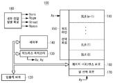
도 2는, 본 발명의 제1 실시예에 관한 플래시 메모리의 구성을 나타내는 도면이다.
도 3은, 본 발명의 제1 실시예에 관한 메모리 셀 어레이의 NAND 스트링의 구성을 나타내는 회로도이다.
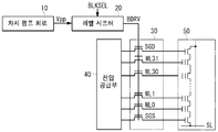
도 4는, 본 발명의 제1 실시예에 관한 워드라인 선택 회로의 구성을 나타내는 도면이다.
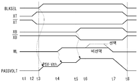
도 5는, 본 발명의 제1 실시예에 관한 워드라인 선택 회로의 동작을 설명하는 파형도이다.
도 6은, 본 발명의 제1 실시예에 관한 메모리 셀 어레이의 블록과 블록 선택부의 관계를 나타내는 레이아웃도이다.
도 7은, 본 발명의 제2 실시예에 관한 메모리 셀 어레이의 블록과 레벨 시프터의 관계를 나타내는 레이아웃도이다.
도 8은, 본 발명의 제2 실시예에 관한 선택된 블록의 워드라인의 구동 방법을 설명하는 도면이다.
110: 메모리 셀 어레이
120: 입출력 버퍼
130: 어드레스 레지스터
140: 제어부
150: 워드라인 선택 회로
160: 페이지 버퍼/센스 회로
170: 열 선택 회로
180: 내부 전압 발생 회로
200: 블록 선택부
210: 레벨 시프터
220: 승압 회로
230: 블록 선택 트랜지스터
Claims (13)
- 복수의 블록을 포함하는 메모리 셀 어레이와,
행 어드레스 정보에 기초하여 상기 메모리 셀 어레이의 블록을 선택하는 블록 선택 수단을 포함하고,
상기 블록 선택 수단은, 블록의 각 워드라인에 접속된 복수의 선택 트랜지스터와,
상기 복수의 선택 트랜지스터의 각 게이트에 접속된 접속 노드를 충전하는 제1 회로와,
상기 제1 회로에 접속되어 상기 접속 노드의 전압을 승압하는 제2 회로와,
상기 복수의 선택 트랜지스터의 한쪽 단자에 동작 전압을 공급하는 공급 수단을 가지며,
상기 접속 노드는, 상기 공급 수단에 의해 공급된 동작 전압에 따라 제1 부스트가 이루어진 후, 상기 제2 회로에 의해 제2 부스트가 이루어지는 비휘발성 반도체 기억 장치. - 청구항 1에 있어서,
상기 제2 회로는 상기 접속 노드에 접속된 커패시터를 포함하고, 상기 제2 회로는 상기 제1 회로로부터 출력되는 전압을 상기 커패시터에 공급하는 비휘발성 반도체 기억 장치. - 청구항 2에 있어서,
상기 제2 회로는 상기 제1 회로와의 사이에 접속된 제1 트랜지스터를 포함하고, 상기 제1 트랜지스터가 도통 상태가 되었을 때, 상기 제1 회로로부터 출력되는 전압이 상기 제1 트랜지스터를 통해 상기 커패시터의 한쪽 전극에 공급되는 비휘발성 반도체 기억 장치. - 청구항 3에 있어서,
상기 제1 트랜지스터의 온/오프 스위칭을 복수회 행함으로써, 상기 커패시터의 한쪽 전극의 충방전을 복수회 반복함으로써, 상기 접속 노드의 승압을 복수회 행하는 비휘발성 반도체 기억 장치. - 청구항 1 내지 청구항 4 중 어느 한 항에 있어서,
상기 제2 회로는 상기 제1 회로와의 사이에 접속된 제2 트랜지스터를 포함하고, 상기 제2 트랜지스터가 도통 상태가 되었을 때, 상기 제1 회로로부터 출력되는 전압이 상기 제2 트랜지스터를 통해 상기 접속 노드에 충전되는 비휘발성 반도체 기억 장치. - 청구항 1 내지 청구항 4 중 어느 한 항에 있어서,
상기 제1 회로는, 차지 펌프 회로로부터 공급된 고전압에 기초하여 제1 전압을 출력하는 레벨 시프터를 포함하는 비휘발성 반도체 기억 장치. - 청구항 1 내지 청구항 4 중 어느 한 항에 있어서,
상기 메모리 셀 어레이는 m행×n열의 블록을 포함하고(m, n은 2 이상의 정수), 상기 제1 회로는 하나의 행의 블록에 공통인 비휘발성 반도체 기억 장치. - 청구항 1 내지 청구항 4 중 어느 한 항에 있어서,
상기 복수의 블록 각각이 제2 회로를 포함하는 비휘발성 반도체 기억 장치. - 청구항 1 내지 청구항 4 중 어느 한 항에 있어서,
제1 부스트가 될 때의 상기 동작 전압은, NAND 스트링을 도통 가능하게 하기 위한 중간 전압인 비휘발성 반도체 기억 장치. - 청구항 9에 있어서,
상기 공급 수단은, 상기 중간 전압의 공급 후에 선택 워드라인에 프로그램 전압을 공급하고, 프로그램 전압은 제2 부스트가 된 선택 트랜지스터를 통해 선택 워드라인에 공급되는 비휘발성 반도체 기억 장치. - 행 어드레스 정보에 응답하여, 메모리 셀 어레이의 블록을 선택하기 위한 복수의 블록 선택 트랜지스터의 각 게이트에 제1 전압을 충전하고,
상기 복수의 블록 선택 트랜지스터의 한쪽 단자에 각 워드라인에 요구되는 동작 전압을 공급함으로써 상기 각 게이트의 제1 전압을 제2 전압으로 승압하고,
상기 각 게이트에 접속된 커패시터에 전압을 공급함으로써 상기 커패시터를 통해 제2 전압을 제3 전압으로 승압하는 단계를 포함하는 비휘발성 반도체 기억 장치의 워드라인의 구동 방법. - 청구항 11에 있어서,
상기 커패시터에 공급되는 전압은 상기 제1 전압이고, 상기 동작 전압은 NAND 스트링을 도통 가능하게 하기 위한 중간 전압인 워드라인의 구동 방법. - 청구항 11에 있어서,
상기 제1 전압은, 차지 펌프 회로로부터 고전압이 공급된 레벨 시프터에 의해 충전되고,
상기 제2 전압에서 상기 제3 전압으로의 승압은, 상기 레벨 시프터로부터 출력되는 전압을 이용하는 승압 회로에 의해 이루어지는 워드라인의 구동 방법.
Applications Claiming Priority (2)
| Application Number | Priority Date | Filing Date | Title |
|---|---|---|---|
| JPJP-P-2016-121359 | 2016-06-20 | ||
| JP2016121359A JP2017228325A (ja) | 2016-06-20 | 2016-06-20 | 不揮発性半導体記憶装置 |
Publications (2)
| Publication Number | Publication Date |
|---|---|
| KR20170142881A true KR20170142881A (ko) | 2017-12-28 |
| KR102046073B1 KR102046073B1 (ko) | 2019-11-18 |
Family
ID=60660384
Family Applications (1)
| Application Number | Title | Priority Date | Filing Date |
|---|---|---|---|
| KR1020170069215A Active KR102046073B1 (ko) | 2016-06-20 | 2017-06-02 | 비휘발성 반도체 기억 장치 및 그 워드라인의 구동 방법 |
Country Status (5)
| Country | Link |
|---|---|
| US (1) | US10269409B2 (ko) |
| JP (1) | JP2017228325A (ko) |
| KR (1) | KR102046073B1 (ko) |
| CN (1) | CN107527654B (ko) |
| TW (1) | TWI637400B (ko) |
Families Citing this family (12)
| Publication number | Priority date | Publication date | Assignee | Title |
|---|---|---|---|---|
| JP6170596B1 (ja) * | 2016-06-15 | 2017-07-26 | ウィンボンド エレクトロニクス コーポレーション | 半導体装置 |
| KR102665270B1 (ko) * | 2016-11-09 | 2024-05-13 | 에스케이하이닉스 주식회사 | 반도체 메모리 장치 및 그것의 동작 방법 |
| IT201600121631A1 (it) * | 2016-11-30 | 2018-05-30 | St Microelectronics Srl | Dispositivo di memoria a cambiamento di fase con un circuito di pilotaggio di linea di parola a elevata velocita' |
| US12199323B2 (en) | 2017-11-28 | 2025-01-14 | Kyocera Corporation | Fuel cell system and equipment management method |
| JP6501325B1 (ja) * | 2018-01-30 | 2019-04-17 | ウィンボンド エレクトロニクス コーポレーション | 半導体記憶装置 |
| JP6588116B2 (ja) | 2018-02-26 | 2019-10-09 | ウィンボンド エレクトロニクス コーポレーション | レベルシフタ |
| JP6535784B1 (ja) | 2018-04-25 | 2019-06-26 | ウィンボンド エレクトロニクス コーポレーション | 半導体記憶装置 |
| US11270746B2 (en) * | 2019-08-22 | 2022-03-08 | Micron Technology, Inc. | Word line driver circuitry, and associated methods, devices, and systems |
| JP2021044041A (ja) * | 2019-09-12 | 2021-03-18 | キオクシア株式会社 | 半導体記憶装置 |
| KR102911991B1 (ko) | 2020-01-20 | 2026-01-12 | 삼성전자 주식회사 | 메모리 장치의 워드라인 구동 회로 및 그것의 동작 방법 |
| CN113724766B (zh) * | 2020-05-26 | 2023-12-29 | 华邦电子股份有限公司 | 半导体存储装置及快闪存储器的运行方法 |
| KR20230146929A (ko) | 2022-04-13 | 2023-10-20 | 에스케이하이닉스 주식회사 | 내부전압생성회로 |
Citations (11)
| Publication number | Priority date | Publication date | Assignee | Title |
|---|---|---|---|---|
| JP2000113691A (ja) * | 1998-10-05 | 2000-04-21 | Nec Corp | 半導体記憶装置のブースト回路と該回路を用いたRowデコーダ電源電位の昇圧方法 |
| JP2002197882A (ja) | 2000-11-18 | 2002-07-12 | Samsung Electronics Co Ltd | メモリセルデコーダ、これを備える半導体メモリ装置および不揮発性半導体メモリ装置の高電圧供給方法 |
| US20030043686A1 (en) * | 2001-08-28 | 2003-03-06 | Samsung Electronics Co., Ltd. | Non-volatile semiconductor memory device having shared row selection circuit |
| US20030133326A1 (en) * | 2002-01-16 | 2003-07-17 | Kabushiki Kaisha Toshiba | Semiconductor memory device |
| JP2004227736A (ja) * | 2003-01-27 | 2004-08-12 | Renesas Technology Corp | 不揮発性半導体記憶装置 |
| JP2008186498A (ja) * | 2007-01-29 | 2008-08-14 | Sanyo Electric Co Ltd | スイッチ駆動回路及びワード線駆動回路 |
| US20130077412A1 (en) * | 2011-09-26 | 2013-03-28 | Elpida Memory, Inc. | Row driver circuit for nand memories including a decoupling inverter |
| US20130088284A1 (en) * | 2011-10-05 | 2013-04-11 | SK Hynix Inc. | Semiconductor device |
| JP2013073657A (ja) * | 2011-09-28 | 2013-04-22 | Winbond Electronics Corp | 半導体記憶装置 |
| US20150255162A1 (en) * | 2014-03-10 | 2015-09-10 | Kabushiki Kaisha Toshiba | Semiconductor memory device and method for detecting leak current |
| US20170084335A1 (en) * | 2015-09-22 | 2017-03-23 | Wook-ghee Hahn | Row decoder and a memory device having the same |
Family Cites Families (18)
| Publication number | Priority date | Publication date | Assignee | Title |
|---|---|---|---|---|
| US6208561B1 (en) | 2000-06-13 | 2001-03-27 | Advanced Micro Devices, Inc. | Method to reduce capacitive loading in flash memory X-decoder for accurate voltage control at wordlines and select lines |
| JP2003141885A (ja) * | 2001-11-01 | 2003-05-16 | Toshiba Corp | 半導体装置 |
| KR100535650B1 (ko) * | 2002-07-15 | 2005-12-08 | 주식회사 하이닉스반도체 | 플래쉬 메모리 장치의 블럭 선택 회로 |
| KR100559715B1 (ko) * | 2004-02-25 | 2006-03-10 | 주식회사 하이닉스반도체 | 낸드 플래시 메모리 소자의 소거 방법 |
| KR100609576B1 (ko) * | 2004-10-05 | 2006-08-09 | 에스티마이크로일렉트로닉스 엔.브이. | 플래쉬 메모리 소자의 블럭 스위치 |
| KR100624302B1 (ko) * | 2004-10-07 | 2006-09-19 | 주식회사 하이닉스반도체 | 난드 플래시 메모리의 로우 디코더 회로 및 이를 이용한동작 전압 공급 방법 |
| US7126862B2 (en) | 2005-03-08 | 2006-10-24 | Spansion Llc | Decoder for memory device |
| KR100699852B1 (ko) * | 2005-07-14 | 2007-03-27 | 삼성전자주식회사 | Hpmos를 이용한 불휘발성 메모리 장치의 워드라인디코더 |
| US20070170979A1 (en) * | 2005-11-25 | 2007-07-26 | Giovanni Campardo | Charge pump systems and methods |
| JP4976764B2 (ja) * | 2006-07-05 | 2012-07-18 | 株式会社東芝 | 半導体記憶装置 |
| US7719919B2 (en) * | 2007-03-20 | 2010-05-18 | Kabushiki Kaisha Toshiba | Semiconductor memory device in which word lines are driven from either side of memory cell array |
| KR100885785B1 (ko) * | 2007-09-10 | 2009-02-26 | 주식회사 하이닉스반도체 | 플래시 메모리 소자의 프로그램 방법 |
| US8068365B2 (en) * | 2008-02-04 | 2011-11-29 | Mosaid Technologies Incorporated | Non-volatile memory device having configurable page size |
| JP2011044222A (ja) * | 2009-07-22 | 2011-03-03 | Toshiba Corp | Nand型フラッシュメモリ |
| US8958244B2 (en) * | 2012-10-16 | 2015-02-17 | Conversant Intellectual Property Management Inc. | Split block decoder for a nonvolatile memory device |
| KR102012903B1 (ko) * | 2012-10-30 | 2019-08-21 | 삼성전자주식회사 | 불휘발성 메모리 장치 및 불휘발성 메모리 장치의 프로그램 방법 |
| KR102103544B1 (ko) * | 2013-01-22 | 2020-04-23 | 삼성전자주식회사 | 고전압 스위치 및 그것을 포함하는 불휘발성 메모리 장치 |
| KR20140139265A (ko) * | 2013-05-27 | 2014-12-05 | 에스케이하이닉스 주식회사 | 블록 선택 회로 및 이를 포함하는 반도체 장치 |
-
2016
- 2016-06-20 JP JP2016121359A patent/JP2017228325A/ja active Pending
-
2017
- 2017-03-22 TW TW106109551A patent/TWI637400B/zh active
- 2017-04-13 CN CN201710238959.2A patent/CN107527654B/zh active Active
- 2017-06-02 KR KR1020170069215A patent/KR102046073B1/ko active Active
- 2017-06-05 US US15/613,285 patent/US10269409B2/en active Active
Patent Citations (11)
| Publication number | Priority date | Publication date | Assignee | Title |
|---|---|---|---|---|
| JP2000113691A (ja) * | 1998-10-05 | 2000-04-21 | Nec Corp | 半導体記憶装置のブースト回路と該回路を用いたRowデコーダ電源電位の昇圧方法 |
| JP2002197882A (ja) | 2000-11-18 | 2002-07-12 | Samsung Electronics Co Ltd | メモリセルデコーダ、これを備える半導体メモリ装置および不揮発性半導体メモリ装置の高電圧供給方法 |
| US20030043686A1 (en) * | 2001-08-28 | 2003-03-06 | Samsung Electronics Co., Ltd. | Non-volatile semiconductor memory device having shared row selection circuit |
| US20030133326A1 (en) * | 2002-01-16 | 2003-07-17 | Kabushiki Kaisha Toshiba | Semiconductor memory device |
| JP2004227736A (ja) * | 2003-01-27 | 2004-08-12 | Renesas Technology Corp | 不揮発性半導体記憶装置 |
| JP2008186498A (ja) * | 2007-01-29 | 2008-08-14 | Sanyo Electric Co Ltd | スイッチ駆動回路及びワード線駆動回路 |
| US20130077412A1 (en) * | 2011-09-26 | 2013-03-28 | Elpida Memory, Inc. | Row driver circuit for nand memories including a decoupling inverter |
| JP2013073657A (ja) * | 2011-09-28 | 2013-04-22 | Winbond Electronics Corp | 半導体記憶装置 |
| US20130088284A1 (en) * | 2011-10-05 | 2013-04-11 | SK Hynix Inc. | Semiconductor device |
| US20150255162A1 (en) * | 2014-03-10 | 2015-09-10 | Kabushiki Kaisha Toshiba | Semiconductor memory device and method for detecting leak current |
| US20170084335A1 (en) * | 2015-09-22 | 2017-03-23 | Wook-ghee Hahn | Row decoder and a memory device having the same |
Also Published As
| Publication number | Publication date |
|---|---|
| CN107527654A (zh) | 2017-12-29 |
| US20170365325A1 (en) | 2017-12-21 |
| JP2017228325A (ja) | 2017-12-28 |
| US10269409B2 (en) | 2019-04-23 |
| KR102046073B1 (ko) | 2019-11-18 |
| CN107527654B (zh) | 2021-04-20 |
| TW201801075A (zh) | 2018-01-01 |
| TWI637400B (zh) | 2018-10-01 |
Similar Documents
| Publication | Publication Date | Title |
|---|---|---|
| KR102046073B1 (ko) | 비휘발성 반도체 기억 장치 및 그 워드라인의 구동 방법 | |
| JP5736441B2 (ja) | Nandフラッシュメモリにおける階層的な共通ソース線構造 | |
| KR100381962B1 (ko) | 비휘발성 메모리 장치의 로우 디코더 | |
| US8994440B2 (en) | Voltage select circuit and intergrated circuit including the same | |
| US9922715B2 (en) | Non-volatile split gate memory device and a method of operating same | |
| US8233328B2 (en) | Nonvolatile semiconductor memory | |
| JP6313244B2 (ja) | 半導体記憶装置 | |
| JP5249394B2 (ja) | 半導体記憶装置 | |
| JP5883494B1 (ja) | 不揮発性半導体記憶装置 | |
| KR102302591B1 (ko) | 사이즈를 감소시킨 로우 디코더 및 이를 포함하는 메모리 장치 | |
| US10083755B2 (en) | Discharge circuit and semiconductor memory device | |
| JP2006309890A (ja) | 不揮発性半導体記憶装置 | |
| US9865358B2 (en) | Flash memory device and erase method thereof capable of reducing power consumption | |
| US8369146B2 (en) | Block decoder of semiconductor memory device | |
| US9564231B2 (en) | Non-volatile memory device and corresponding operating method with stress reduction | |
| US6166982A (en) | High voltage switch for eeprom/flash memories | |
| JP4909647B2 (ja) | 不揮発性半導体記憶装置 | |
| KR20180097110A (ko) | 양(+) 및/또는 음(-) 전압 발생 회로를 포함하는 반도체 장치 | |
| JP6744893B2 (ja) | 不揮発性半導体記憶装置 | |
| KR20030009289A (ko) | 3층 금속 상호연결을 적용한 플래시 메모리 구조 | |
| JP2013198308A (ja) | 電圧生成回路 |
Legal Events
| Date | Code | Title | Description |
|---|---|---|---|
| A201 | Request for examination | ||
| PA0109 | Patent application |
Patent event code: PA01091R01D Comment text: Patent Application Patent event date: 20170602 |
|
| PA0201 | Request for examination | ||
| PG1501 | Laying open of application | ||
| E902 | Notification of reason for refusal | ||
| PE0902 | Notice of grounds for rejection |
Comment text: Notification of reason for refusal Patent event date: 20181022 Patent event code: PE09021S01D |
|
| E90F | Notification of reason for final refusal | ||
| PE0902 | Notice of grounds for rejection |
Comment text: Final Notice of Reason for Refusal Patent event date: 20190418 Patent event code: PE09021S02D |
|
| E701 | Decision to grant or registration of patent right | ||
| PE0701 | Decision of registration |
Patent event code: PE07011S01D Comment text: Decision to Grant Registration Patent event date: 20191026 |
|
| GRNT | Written decision to grant | ||
| PR0701 | Registration of establishment |
Comment text: Registration of Establishment Patent event date: 20191112 Patent event code: PR07011E01D |
|
| PR1002 | Payment of registration fee |
Payment date: 20191113 End annual number: 3 Start annual number: 1 |
|
| PG1601 | Publication of registration | ||
| PR1001 | Payment of annual fee |
Payment date: 20221102 Start annual number: 4 End annual number: 4 |
|
| PR1001 | Payment of annual fee |
Payment date: 20231101 Start annual number: 5 End annual number: 5 |