KR20170143069A - 두께 측정 장치 및 두께 측정 방법 - Google Patents
두께 측정 장치 및 두께 측정 방법 Download PDFInfo
- Publication number
- KR20170143069A KR20170143069A KR1020160075906A KR20160075906A KR20170143069A KR 20170143069 A KR20170143069 A KR 20170143069A KR 1020160075906 A KR1020160075906 A KR 1020160075906A KR 20160075906 A KR20160075906 A KR 20160075906A KR 20170143069 A KR20170143069 A KR 20170143069A
- Authority
- KR
- South Korea
- Prior art keywords
- optical coupler
- target
- line
- signal
- reference mirror
- Prior art date
- Legal status (The legal status is an assumption and is not a legal conclusion. Google has not performed a legal analysis and makes no representation as to the accuracy of the status listed.)
- Granted
Links
Images





Classifications
-
- G—PHYSICS
- G01—MEASURING; TESTING
- G01B—MEASURING LENGTH, THICKNESS OR SIMILAR LINEAR DIMENSIONS; MEASURING ANGLES; MEASURING AREAS; MEASURING IRREGULARITIES OF SURFACES OR CONTOURS
- G01B9/00—Measuring instruments characterised by the use of optical techniques
- G01B9/02—Interferometers
- G01B9/02001—Interferometers characterised by controlling or generating intrinsic radiation properties
-
- G—PHYSICS
- G01—MEASURING; TESTING
- G01B—MEASURING LENGTH, THICKNESS OR SIMILAR LINEAR DIMENSIONS; MEASURING ANGLES; MEASURING AREAS; MEASURING IRREGULARITIES OF SURFACES OR CONTOURS
- G01B11/00—Measuring arrangements characterised by the use of optical techniques
- G01B11/02—Measuring arrangements characterised by the use of optical techniques for measuring length, width or thickness
- G01B11/06—Measuring arrangements characterised by the use of optical techniques for measuring length, width or thickness for measuring thickness ; e.g. of sheet material
-
- G—PHYSICS
- G01—MEASURING; TESTING
- G01B—MEASURING LENGTH, THICKNESS OR SIMILAR LINEAR DIMENSIONS; MEASURING ANGLES; MEASURING AREAS; MEASURING IRREGULARITIES OF SURFACES OR CONTOURS
- G01B11/00—Measuring arrangements characterised by the use of optical techniques
- G01B11/02—Measuring arrangements characterised by the use of optical techniques for measuring length, width or thickness
- G01B11/06—Measuring arrangements characterised by the use of optical techniques for measuring length, width or thickness for measuring thickness ; e.g. of sheet material
- G01B11/0616—Measuring arrangements characterised by the use of optical techniques for measuring length, width or thickness for measuring thickness ; e.g. of sheet material of coating
-
- G—PHYSICS
- G01—MEASURING; TESTING
- G01B—MEASURING LENGTH, THICKNESS OR SIMILAR LINEAR DIMENSIONS; MEASURING ANGLES; MEASURING AREAS; MEASURING IRREGULARITIES OF SURFACES OR CONTOURS
- G01B11/00—Measuring arrangements characterised by the use of optical techniques
- G01B11/02—Measuring arrangements characterised by the use of optical techniques for measuring length, width or thickness
- G01B11/06—Measuring arrangements characterised by the use of optical techniques for measuring length, width or thickness for measuring thickness ; e.g. of sheet material
- G01B11/0616—Measuring arrangements characterised by the use of optical techniques for measuring length, width or thickness for measuring thickness ; e.g. of sheet material of coating
- G01B11/0625—Measuring arrangements characterised by the use of optical techniques for measuring length, width or thickness for measuring thickness ; e.g. of sheet material of coating with measurement of absorption or reflection
-
- G—PHYSICS
- G01—MEASURING; TESTING
- G01B—MEASURING LENGTH, THICKNESS OR SIMILAR LINEAR DIMENSIONS; MEASURING ANGLES; MEASURING AREAS; MEASURING IRREGULARITIES OF SURFACES OR CONTOURS
- G01B11/00—Measuring arrangements characterised by the use of optical techniques
- G01B11/02—Measuring arrangements characterised by the use of optical techniques for measuring length, width or thickness
- G01B11/06—Measuring arrangements characterised by the use of optical techniques for measuring length, width or thickness for measuring thickness ; e.g. of sheet material
- G01B11/0616—Measuring arrangements characterised by the use of optical techniques for measuring length, width or thickness for measuring thickness ; e.g. of sheet material of coating
- G01B11/0675—Measuring arrangements characterised by the use of optical techniques for measuring length, width or thickness for measuring thickness ; e.g. of sheet material of coating using interferometry
-
- G—PHYSICS
- G01—MEASURING; TESTING
- G01B—MEASURING LENGTH, THICKNESS OR SIMILAR LINEAR DIMENSIONS; MEASURING ANGLES; MEASURING AREAS; MEASURING IRREGULARITIES OF SURFACES OR CONTOURS
- G01B9/00—Measuring instruments characterised by the use of optical techniques
- G01B9/02—Interferometers
- G01B9/02015—Interferometers characterised by the beam path configuration
- G01B9/02017—Interferometers characterised by the beam path configuration with multiple interactions between the target object and light beams, e.g. beam reflections occurring from different locations
- G01B9/02021—Interferometers characterised by the beam path configuration with multiple interactions between the target object and light beams, e.g. beam reflections occurring from different locations contacting different faces of object, e.g. opposite faces
-
- G—PHYSICS
- G02—OPTICS
- G02B—OPTICAL ELEMENTS, SYSTEMS OR APPARATUS
- G02B6/00—Light guides; Structural details of arrangements comprising light guides and other optical elements, e.g. couplings
- G02B6/24—Coupling light guides
- G02B6/26—Optical coupling means
- G02B6/262—Optical details of coupling light into, or out of, or between fibre ends, e.g. special fibre end shapes or associated optical elements
-
- H—ELECTRICITY
- H01—ELECTRIC ELEMENTS
- H01S—DEVICES USING THE PROCESS OF LIGHT AMPLIFICATION BY STIMULATED EMISSION OF RADIATION [LASER] TO AMPLIFY OR GENERATE LIGHT; DEVICES USING STIMULATED EMISSION OF ELECTROMAGNETIC RADIATION IN WAVE RANGES OTHER THAN OPTICAL
- H01S3/00—Lasers, i.e. devices using stimulated emission of electromagnetic radiation in the infrared, visible or ultraviolet wave range
- H01S3/10—Controlling the intensity, frequency, phase, polarisation or direction of the emitted radiation, e.g. switching, gating, modulating or demodulating
- H01S3/10038—Amplitude control
- H01S3/10046—Pulse repetition rate control
-
- G—PHYSICS
- G01—MEASURING; TESTING
- G01B—MEASURING LENGTH, THICKNESS OR SIMILAR LINEAR DIMENSIONS; MEASURING ANGLES; MEASURING AREAS; MEASURING IRREGULARITIES OF SURFACES OR CONTOURS
- G01B2210/00—Aspects not specifically covered by any group under G01B, e.g. of wheel alignment, caliper-like sensors
- G01B2210/56—Measuring geometric parameters of semiconductor structures, e.g. profile, critical dimensions or trench depth
Landscapes
- Physics & Mathematics (AREA)
- General Physics & Mathematics (AREA)
- Optics & Photonics (AREA)
- Electromagnetism (AREA)
- Engineering & Computer Science (AREA)
- Plasma & Fusion (AREA)
- Length Measuring Devices By Optical Means (AREA)
Abstract
Description
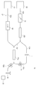
도 1b는 본 발명의 실시예에 따른 두께 측정 장치를 개략적으로 보여주는 도면이다.
도 2는 타겟의 일 실시예를 보여주는 도면이다.
도 3은 도 1a의 두께 측정 장치를 이용하여, 도 2의 타겟의 두께를 측정하는 과정을 보여주는 플로우차트이다.
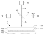
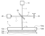
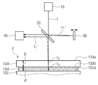
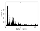
도 4a 내지 도 4f는 도 3의 두께 측정 방법을 보여주는 도면들이다.
Claims (10)
- 펨토초 레이저 광을 방출하는 광원;
상기 펨토초 레이저 광의 일부를 타겟으로 입사시키고, 다른 일부를 기준 거울로 입사시키는 광 커플러;
상기 기준 거울에서 반사된 반사 신호 및 상기 타겟에서 발생된 샘플 신호가 입사되고, 상기 반사 신호와 상기 샘플 신호간의 간섭 신호로부터 상기 타겟의 두께를 측정하는 검출기; 및
상기 광원, 상기 광 커플러, 그리고 상기 검출기를 연결하는 광 파이버를 포함하는 두께 측정 장치.
- 제 1 항에 있어서,
상기 광 커플러의 일단은 상기 광원 및 상기 검출기와 연결되고, 상기 광 커플러의 타단은 상기 타겟 및 상기 기준 거울과 인접하는 두께 측정 장치.
- 제 2 항에 있어서,
상기 광 파이버는:
상기 광 커플러의 일단과 상기 광원을 연결하는 제 1 라인;
상기 광 커플러의 일단과 상기 검출기를 연결하는 제 2 라인;
상기 광 커플러의 타단으로부터 상기 타겟으로 연장되는 제 3 라인; 및
상기 광 커플러의 타단으로부터 상기 기준 거울로 연장되는 제 4 라인을 포함하는 두께 측정 장치.
- 제 1 항에 있어서,
상기 광 커플러는 제 1 광 커플러이고,
상기 두께 측정 장치는, 상기 제 1 광 커플러와 상기 검출기 사이의 상기 광 파이버 상에 배치된 제 2 광 커플러를 더 포함하는 두께 측정 장치.
- 제 4 항에 있어서,
상기 광 파이버는:
상기 제 1 광 커플러의 일단과 상기 광원을 연결하는 제 1 라인;
상기 제 2 광 커플러의 일단과 상기 검출기를 연결하는 제 2 라인;
상기 제 1 광 커플러의 타단으로부터 상기 타겟으로 연장되는 제 3 라인;
상기 제 1 광 커플러의 타단으로부터 상기 기준 거울로 연장되는 제 4 라인;
상기 제 2 광 커플러의 타단으로부터 상기 타겟으로 연장되는 제 5 라인; 및
상기 제 1 광 커플러의 일단과 상기 제 2 광 커플러의 타단을 연결하는 제 6 라인을 포함하는 두께 측정 장치.
- 제 5 항에 있어서,
상기 제 3 라인 및 상기 제 5 라인의 단부들은, 상기 타겟을 중심으로 서로 대향되게 배치되는 두께 측정 장치.
- 제 1 항에 있어서,
상기 펨토초 레이저의 입사 방향을 따라 상기 기준 거울을 이동시키는 기준 거울 이동부를 더 포함하는 두께 측정 장치.
- 제 1 항에 있어서,
상기 샘플 신호는 상기 타겟으로부터 반사된 반사 신호인 두께 측정 장치.
- 제 1 항에 있어서,
상기 샘플 신호는 상기 타겟을 투과한 투과 신호인 두께 측정 장치.
- 펨토초 레이저 광을 방출하는 것;
상기 펨토초 레이저 광의 일부를 기준 거울로 입사하는 것;
상기 펨토초 레이저 광의 다른 일부를 적층 구조체로 입사하는 것;
상기 기준 거울에서 반사된 기준 신호를 획득하는 것;
상기 적층 구조체로부터 샘플 신호들을 획득하는 것;
상기 기준 신호와 상기 샘플 신호들 간의 간섭 신호들을 획득하는 것; 및
상기 간섭 신호들로부터 상기 적층 구조체의 두께를 측정하는 것을 포함하되,
상기 간섭 신호들로부터 상기 적층 구조체의 두께를 측정하는 것은, 상기 간섭 신호들의 피크점들로부터 상기 적층 구조체의 각각의 층들의 두께들로 변환하는 것을 포함하는 두께 측정 방법.
Priority Applications (2)
| Application Number | Priority Date | Filing Date | Title |
|---|---|---|---|
| KR1020160075906A KR102594111B1 (ko) | 2016-06-17 | 2016-06-17 | 두께 측정 장치 및 두께 측정 방법 |
| US15/464,896 US10088297B2 (en) | 2016-06-17 | 2017-03-21 | Apparatus and method for measuring thickness |
Applications Claiming Priority (1)
| Application Number | Priority Date | Filing Date | Title |
|---|---|---|---|
| KR1020160075906A KR102594111B1 (ko) | 2016-06-17 | 2016-06-17 | 두께 측정 장치 및 두께 측정 방법 |
Publications (2)
| Publication Number | Publication Date |
|---|---|
| KR20170143069A true KR20170143069A (ko) | 2017-12-29 |
| KR102594111B1 KR102594111B1 (ko) | 2023-10-26 |
Family
ID=60660018
Family Applications (1)
| Application Number | Title | Priority Date | Filing Date |
|---|---|---|---|
| KR1020160075906A Active KR102594111B1 (ko) | 2016-06-17 | 2016-06-17 | 두께 측정 장치 및 두께 측정 방법 |
Country Status (2)
| Country | Link |
|---|---|
| US (1) | US10088297B2 (ko) |
| KR (1) | KR102594111B1 (ko) |
Cited By (3)
| Publication number | Priority date | Publication date | Assignee | Title |
|---|---|---|---|---|
| KR20200105597A (ko) * | 2019-02-28 | 2020-09-08 | 전남대학교산학협력단 | 광 커플러를 이용한 수질 오염 측정 시스템 |
| KR20210014947A (ko) | 2019-07-31 | 2021-02-10 | 에스케이하이닉스 주식회사 | 두께 측정 장치 및 방법 |
| WO2022065758A1 (ko) * | 2020-09-25 | 2022-03-31 | 한국기계연구원 | 다중대상 거리측정 시스템 및 이를 이용한 다중대상 거리측정 방법 |
Families Citing this family (1)
| Publication number | Priority date | Publication date | Assignee | Title |
|---|---|---|---|---|
| FR3064349B1 (fr) * | 2017-03-21 | 2023-06-30 | Fogale Nanotech | Dispositif et procede de reflectometrie a faible coherence a detection temps-frequence |
Citations (4)
| Publication number | Priority date | Publication date | Assignee | Title |
|---|---|---|---|---|
| JPS574150B2 (ko) * | 1972-11-02 | 1982-01-25 | ||
| US20070127034A1 (en) * | 2005-12-06 | 2007-06-07 | Tokyo Electron Limited | Method for measuring physical quantity of measurement object in substrate processing apparatus and storage medium storing program for implementing the method |
| JP5199141B2 (ja) * | 2009-02-02 | 2013-05-15 | 株式会社神戸製鋼所 | 形状測定装置 |
| JP2015075356A (ja) * | 2013-10-07 | 2015-04-20 | 関西ペイント株式会社 | 膜厚測定方法および膜厚測定装置 |
Family Cites Families (14)
| Publication number | Priority date | Publication date | Assignee | Title |
|---|---|---|---|---|
| US5091647A (en) | 1990-12-24 | 1992-02-25 | Ford Motor Company | Method and apparatus for measuring the thickness of a layer on a substrate |
| KR100673880B1 (ko) | 2000-07-20 | 2007-01-25 | 주식회사 하이닉스반도체 | 광학적 방법을 이용한 금속막 두께 측정 장치 및 그를이용한 금속막 두께 측정 방법 |
| WO2009009178A2 (en) * | 2007-04-06 | 2009-01-15 | The General Hospital Corporation | Systems and methods for optical imaging using early arriving photons |
| US8672480B2 (en) * | 2009-09-30 | 2014-03-18 | Nidek Co., Ltd. | Ophthalmic photographing apparatus |
| TW201314194A (zh) | 2011-09-28 | 2013-04-01 | Ind Tech Res Inst | 物件特性量測系統 |
| JP6143422B2 (ja) * | 2012-03-30 | 2017-06-07 | キヤノン株式会社 | 画像処理装置及びその方法 |
| US20140186212A1 (en) * | 2012-11-13 | 2014-07-03 | Awareness Technology Inc. | Methods and apparatus for measuring luminescence and absorbance |
| KR101388239B1 (ko) | 2012-11-19 | 2014-04-23 | 와이즈플래닛(주) | 카메라와 가변파장 레이저를 이용한 다층막 두께 측정 검사장치 |
| JP5704150B2 (ja) * | 2012-11-21 | 2015-04-22 | 株式会社東京精密 | 白色干渉装置及び白色干渉装置の位置及び変位測定方法 |
| JP2014109481A (ja) * | 2012-11-30 | 2014-06-12 | Canon Inc | 計測方法及び計測装置 |
| KR101434965B1 (ko) | 2013-02-13 | 2014-08-28 | 주식회사 나노베이스 | 두께 측정 시스템 및 그 방법 |
| JP6271243B2 (ja) | 2013-12-20 | 2018-01-31 | 東京エレクトロン株式会社 | 厚さ・温度測定装置、厚さ・温度測定方法及び基板処理システム |
| KR101538028B1 (ko) | 2014-04-11 | 2015-07-22 | 한국기계연구원 | 박막의 가공 두께 제어 및 모니터링을 위한 실시간 측정 및 가공 장치 및 방법 |
| KR101540541B1 (ko) | 2014-08-20 | 2015-07-30 | 현대중공업 주식회사 | 펨토초 레이저 발생장치 및 그와 연동하는 도막두께 측정장치 |
-
2016
- 2016-06-17 KR KR1020160075906A patent/KR102594111B1/ko active Active
-
2017
- 2017-03-21 US US15/464,896 patent/US10088297B2/en active Active
Patent Citations (4)
| Publication number | Priority date | Publication date | Assignee | Title |
|---|---|---|---|---|
| JPS574150B2 (ko) * | 1972-11-02 | 1982-01-25 | ||
| US20070127034A1 (en) * | 2005-12-06 | 2007-06-07 | Tokyo Electron Limited | Method for measuring physical quantity of measurement object in substrate processing apparatus and storage medium storing program for implementing the method |
| JP5199141B2 (ja) * | 2009-02-02 | 2013-05-15 | 株式会社神戸製鋼所 | 形状測定装置 |
| JP2015075356A (ja) * | 2013-10-07 | 2015-04-20 | 関西ペイント株式会社 | 膜厚測定方法および膜厚測定装置 |
Cited By (4)
| Publication number | Priority date | Publication date | Assignee | Title |
|---|---|---|---|---|
| KR20200105597A (ko) * | 2019-02-28 | 2020-09-08 | 전남대학교산학협력단 | 광 커플러를 이용한 수질 오염 측정 시스템 |
| KR20210014947A (ko) | 2019-07-31 | 2021-02-10 | 에스케이하이닉스 주식회사 | 두께 측정 장치 및 방법 |
| US11022427B2 (en) | 2019-07-31 | 2021-06-01 | SK Hynix Inc. | Device and method for measuring thickness |
| WO2022065758A1 (ko) * | 2020-09-25 | 2022-03-31 | 한국기계연구원 | 다중대상 거리측정 시스템 및 이를 이용한 다중대상 거리측정 방법 |
Also Published As
| Publication number | Publication date |
|---|---|
| US10088297B2 (en) | 2018-10-02 |
| KR102594111B1 (ko) | 2023-10-26 |
| US20170363418A1 (en) | 2017-12-21 |
Similar Documents
| Publication | Publication Date | Title |
|---|---|---|
| US7654750B2 (en) | Bidirectional optical fiber link systems component couplers | |
| US8335411B2 (en) | Fiber optic bi-directional coupling lens | |
| US9612402B2 (en) | Integrated sub-wavelength grating system | |
| JP2018005067A (ja) | アライメント用光学測定素子及び該光学測定素子を用いた光プローブのアライメント方法 | |
| CN108351469A (zh) | 硅光路 | |
| US20100329603A1 (en) | Structure and method for aligning an optical fiber and a submicronic waveguide | |
| US10739518B2 (en) | Optical components for wavelength division multiplexing with high-density optical interconnect modules | |
| KR102594111B1 (ko) | 두께 측정 장치 및 두께 측정 방법 | |
| CN106291834A (zh) | 光学通讯装置 | |
| US8744223B2 (en) | Array-type photo module | |
| CN110875782B (zh) | 相干接收器的组装方法 | |
| US9784931B2 (en) | Optical waveguide module | |
| JP6696159B2 (ja) | 光受信器 | |
| CN111505775B (zh) | 光模块 | |
| CN103823281A (zh) | 多通道光接收组件 | |
| KR20120029316A (ko) | 광도파로 디바이스 및 광학식 터치 패널 | |
| CN112073125B (zh) | 一种用于调节波长的器件 | |
| KR20100074704A (ko) | 다파장 분리용 광모듈 | |
| JP5716442B2 (ja) | 多チャネル光受信装置 | |
| CN108241154A (zh) | 一种激光发射接收装置以及激光探测与测量系统 | |
| WO2022236855A1 (zh) | 一种基于膜片分光的高集成度的波分接收器件 | |
| TWI661239B (zh) | Fiber optic module | |
| JP6972563B2 (ja) | 光導波路デバイスの製造方法 | |
| JP6110797B2 (ja) | 受光デバイス | |
| CN121721774A (zh) | 光学组件及电子设备 |
Legal Events
| Date | Code | Title | Description |
|---|---|---|---|
| PA0109 | Patent application |
St.27 status event code: A-0-1-A10-A12-nap-PA0109 |
|
| PG1501 | Laying open of application |
St.27 status event code: A-1-1-Q10-Q12-nap-PG1501 |
|
| A201 | Request for examination | ||
| PA0201 | Request for examination |
St.27 status event code: A-1-2-D10-D11-exm-PA0201 |
|
| D13-X000 | Search requested |
St.27 status event code: A-1-2-D10-D13-srh-X000 |
|
| D14-X000 | Search report completed |
St.27 status event code: A-1-2-D10-D14-srh-X000 |
|
| E902 | Notification of reason for refusal | ||
| PE0902 | Notice of grounds for rejection |
St.27 status event code: A-1-2-D10-D21-exm-PE0902 |
|
| E13-X000 | Pre-grant limitation requested |
St.27 status event code: A-2-3-E10-E13-lim-X000 |
|
| P11-X000 | Amendment of application requested |
St.27 status event code: A-2-2-P10-P11-nap-X000 |
|
| P13-X000 | Application amended |
St.27 status event code: A-2-2-P10-P13-nap-X000 |
|
| E701 | Decision to grant or registration of patent right | ||
| PE0701 | Decision of registration |
St.27 status event code: A-1-2-D10-D22-exm-PE0701 |
|
| PR0701 | Registration of establishment |
St.27 status event code: A-2-4-F10-F11-exm-PR0701 |
|
| PR1002 | Payment of registration fee |
St.27 status event code: A-2-2-U10-U11-oth-PR1002 Fee payment year number: 1 |
|
| PG1601 | Publication of registration |
St.27 status event code: A-4-4-Q10-Q13-nap-PG1601 |