KR20170143084A - 반도체장치 및 반도체시스템 - Google Patents
반도체장치 및 반도체시스템 Download PDFInfo
- Publication number
- KR20170143084A KR20170143084A KR1020160076051A KR20160076051A KR20170143084A KR 20170143084 A KR20170143084 A KR 20170143084A KR 1020160076051 A KR1020160076051 A KR 1020160076051A KR 20160076051 A KR20160076051 A KR 20160076051A KR 20170143084 A KR20170143084 A KR 20170143084A
- Authority
- KR
- South Korea
- Prior art keywords
- data
- signal
- shifting
- circuit
- input
- Prior art date
- Legal status (The legal status is an assumption and is not a legal conclusion. Google has not performed a legal analysis and makes no representation as to the accuracy of the status listed.)
- Ceased
Links
Images


Classifications
-
- G—PHYSICS
- G11—INFORMATION STORAGE
- G11C—STATIC STORES
- G11C29/00—Checking stores for correct operation ; Subsequent repair; Testing stores during standby or offline operation
- G11C29/04—Detection or location of defective memory elements, e.g. cell constructio details, timing of test signals
- G11C29/08—Functional testing, e.g. testing during refresh, power-on self testing [POST] or distributed testing
- G11C29/12—Built-in arrangements for testing, e.g. built-in self testing [BIST] or interconnection details
- G11C29/38—Response verification devices
- G11C29/42—Response verification devices using error correcting codes [ECC] or parity check
-
- G—PHYSICS
- G11—INFORMATION STORAGE
- G11C—STATIC STORES
- G11C7/00—Arrangements for writing information into, or reading information out from, a digital store
- G11C7/10—Input/output [I/O] data interface arrangements, e.g. I/O data control circuits, I/O data buffers
-
- G—PHYSICS
- G06—COMPUTING OR CALCULATING; COUNTING
- G06F—ELECTRIC DIGITAL DATA PROCESSING
- G06F11/00—Error detection; Error correction; Monitoring
- G06F11/07—Responding to the occurrence of a fault, e.g. fault tolerance
- G06F11/08—Error detection or correction by redundancy in data representation, e.g. by using checking codes
- G06F11/10—Adding special bits or symbols to the coded information, e.g. parity check, casting out 9's or 11's
- G06F11/1008—Adding special bits or symbols to the coded information, e.g. parity check, casting out 9's or 11's in individual solid state devices
- G06F11/1048—Adding special bits or symbols to the coded information, e.g. parity check, casting out 9's or 11's in individual solid state devices using arrangements adapted for a specific error detection or correction feature
-
- G—PHYSICS
- G11—INFORMATION STORAGE
- G11C—STATIC STORES
- G11C29/00—Checking stores for correct operation ; Subsequent repair; Testing stores during standby or offline operation
- G11C29/02—Detection or location of defective auxiliary circuits, e.g. defective refresh counters
- G11C29/022—Detection or location of defective auxiliary circuits, e.g. defective refresh counters in I/O circuitry
-
- G—PHYSICS
- G11—INFORMATION STORAGE
- G11C—STATIC STORES
- G11C29/00—Checking stores for correct operation ; Subsequent repair; Testing stores during standby or offline operation
- G11C29/04—Detection or location of defective memory elements, e.g. cell constructio details, timing of test signals
- G11C29/08—Functional testing, e.g. testing during refresh, power-on self testing [POST] or distributed testing
- G11C29/12—Built-in arrangements for testing, e.g. built-in self testing [BIST] or interconnection details
- G11C29/18—Address generation devices; Devices for accessing memories, e.g. details of addressing circuits
-
- G—PHYSICS
- G11—INFORMATION STORAGE
- G11C—STATIC STORES
- G11C29/00—Checking stores for correct operation ; Subsequent repair; Testing stores during standby or offline operation
- G11C29/04—Detection or location of defective memory elements, e.g. cell constructio details, timing of test signals
- G11C29/08—Functional testing, e.g. testing during refresh, power-on self testing [POST] or distributed testing
- G11C29/12—Built-in arrangements for testing, e.g. built-in self testing [BIST] or interconnection details
- G11C29/44—Indication or identification of errors, e.g. for repair
-
- G—PHYSICS
- G11—INFORMATION STORAGE
- G11C—STATIC STORES
- G11C29/00—Checking stores for correct operation ; Subsequent repair; Testing stores during standby or offline operation
- G11C29/52—Protection of memory contents; Detection of errors in memory contents
-
- G—PHYSICS
- G11—INFORMATION STORAGE
- G11C—STATIC STORES
- G11C8/00—Arrangements for selecting an address in a digital store
- G11C8/18—Address timing or clocking circuits; Address control signal generation or management, e.g. for row address strobe [RAS] or column address strobe [CAS] signals
-
- G—PHYSICS
- G11—INFORMATION STORAGE
- G11C—STATIC STORES
- G11C29/00—Checking stores for correct operation ; Subsequent repair; Testing stores during standby or offline operation
- G11C29/04—Detection or location of defective memory elements, e.g. cell constructio details, timing of test signals
- G11C2029/0411—Online error correction
Landscapes
- Engineering & Computer Science (AREA)
- Theoretical Computer Science (AREA)
- Physics & Mathematics (AREA)
- General Engineering & Computer Science (AREA)
- General Physics & Mathematics (AREA)
- Quality & Reliability (AREA)
- Microelectronics & Electronic Packaging (AREA)
- Techniques For Improving Reliability Of Storages (AREA)
- Human Computer Interaction (AREA)
- For Increasing The Reliability Of Semiconductor Memories (AREA)
Abstract
Description
도 2는 도 1 에 도시된 반도체시스템에 포함된 제어회로의 일 실시예에 따른 내부 구성을 도시한 블럭도이다.
도 3은 도 1 에 도시된 반도체시스템에 포함된 데이터변환회로의 일 실시예에 따른 내부 구성을 도시한 블럭도이다.
도 4는 도 3 에 도시된 데이터변환회로에 포함된 래치회로의 동작을 설명하기 위한 표이다.
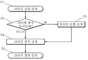
도 5는 본 발명의 일 실시예에 따른 데이터입출력방법의 순서도이다.
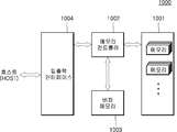
도 6은 도 1 내지 도 5에 도시된 반도체장치 및 반도체시스템이 적용된 전자시스템의 일 실시예에 따른 구성을 도시한 도면이다.
도 7은 도 1 내지 도 5에 도시된 반도체장치 및 반도체시스템이 적용된 전자시스템의 다른 실시예에 따른 구성을 도시한 도면이다.
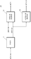
10. 제어회로 11. 카운터
12. 제어신호생성회로 13. 시프팅신호생성회로
20. 데이터입출력회로 21. 에러정정회로
22. 데이터변환회로 30. 메모리영역
221. 래치회로 222. 레지스터
Claims (25)
- 커맨드, 어드레스를 출력하고, 데이터를 입출력하는 제1 반도체장치; 및
상기 커맨드에 응답하여 라이트동작에 진입하고, 상기 데이터의 불량을 정정하며, 상기 어드레스에 따라 선택되는 페이지에 불량이 정정된 상기 데이터 및 상기 데이터의 불량정보를 저장하되, 상기 어드레스의 동일한 조합이 기 설정된 횟수 이상 입력되는 경우 상기 데이터와 상기 데이터의 불량정보를 시프팅하여 상기 페이지에 저장하는 제2 반도체장치를 포함하는 반도체시스템.
- 제 1 항에 있어서, 상기 제2 반도체장치는
상기 라이트동작 중 상기 동일한 조합의 어드레스가 상기 기 설정된 횟수 미만으로 입력되는 경우 상기 페이지에 저장되는 상기 데이터 및 상기 불량정보를 시프팅하지 않고 저장하는 반도체시스템.
- 제 1 항에 있어서, 상기 제2 반도체장치는
리드동작 시 시프팅되어 상기 페이지에 저장된 상기 데이터 및 상기 불량정보의 위치를 복원하고, 상기 불량정보에 의해 상기 데이터의 불량을 정정하여 출력하는 반도체시스템.
- 제 1 항에 있어서, 상기 제2 반도체장치는
상기 커맨드에 응답하여 상기 라이트동작 시 동일한 상기 어드레스의 조합이 상기 기 설정된 횟수 이상 입력되는 경우 발생하는 펄스를 포함하는 제어신호 및 동일한 상기 어드레스의 조합이 상기 기 설정된 횟수 이상 입력되는 경우 카운팅되는 시프팅신호를 생성하는 제어회로; 및
상기 제어신호의 펄스에 응답하여 상기 데이터 및 상기 불량정보를 시프팅하여 내부데이터를 생성하는 데이터입출력회로를 포함하는 반도체시스템.
- 제 4 항에 있어서, 상기 내부데이터는 상기 데이터, 상기 불량정보 및 상기 시프팅신호를 포함하는 반도체시스템.
- 제 4 항에 있어서, 상기 데이터입출력회로는
리드동작 시 상기 시프팅신호에 의해 상기 내부데이터에 포함된 상기 데이터 및 상기 불량정보의 위치를 복원하고, 상기 불량정보에 의해 상기 내부데이터의 불량을 정정하여 상기 데이터로 출력하는 반도체시스템.
- 제 4 항에 있어서, 상기 제어회로는
상기 어드레스가 동일한 조합인 경우 카운팅되는 카운팅신호를 생성하는 카운터;
상기 커맨드에 응답하여 상기 카운팅신호가 상기 기 설정된 횟수이상 카운팅되는 경우 발생하는 펄스를 포함하는 상기 제어신호를 생성하는 제어신호생성회로; 및
상기 카운팅신호가 상기 기 설정된 횟수이상 카운팅되는 경우 카운팅되는 상기 시프팅신호를 생성하는 시프팅신호생성회로를 포함하는 반도체시스템.
- 제 4 항에 있어서, 상기 데이터입출력회로는
상기 라이트동작 시 상기 데이터의 불량을 검출하고, 상기 데이터의 불량을 정정하여 정정데이터를 생성하며, 상기 데이터의 불량정보를 포함하는 패리티신호를 생성하는 에러정정회로; 및
상기 제어신호에 응답하여 상기 정정데이터 및 상기 패리티신호를 시프팅하여 상기 내부데이터를 생성하는 데이터변환회로를 포함하는 반도체시스템.
- 제 8 항에 있어서,
상기 에러정정회로는 리드동작 시 상기 패리티신호에 의해 출력데이터의 불량을 정정하여 상기 데이터로 출력하고,
상기 데이터변환회로는 상기 리드동작 시 상기 시프팅신호에 의해 상기 내부데이터에 포함된 상기 정정데이터 및 상기 패리티신호의 위치를 복원하여 상기 출력데이터를 생성하는 반도체시스템.
- 제 8 항에 있어서, 상기 데이터변환회로는
상기 제어신호의 펄스가 입력되는 횟수만큼 상기 정정데이터와 상기 패리티신호를 시프팅하고, 시프팅 된 상기 정정데이터와 상기 패리티신호 및 상기 시프팅신호를 래치데이터로 출력하는 래치회로; 및
라이트신호에 응답하여 상기 래치데이터를 상기 내부데이터로 출력하는 레지스터를 포함하는 반도체시스템.
- 제 10 항에 있어서,
상기 래치회로는 리드동작 시 상기 래치데이터에 포함된 상기 시프팅신호에 의해 상기 정정데이터와 상기 패리티신호의 위치를 복원하여 상기 출력데이터로 출력하고,
상기 레지스터는 리드신호에 응답하여 상기 내부데이터를 상기 래치데이터로 출력하는 반도체시스템.
- 제 3 항에 있어서, 상기 제2 반도체장치는
상기 라이트동작 시 상기 어드레스의 조합에 따라 선택되는 상기 페이지에 상기 내부데이터를 저장하고, 상기 리드동작 시 상기 어드레스의 조합에 따라 선택되는 상기 페이지에 저장된 상기 내부데이터를 출력하는 메모리영역을 더 포함하는 반도체시스템.
- 라이트동작 시 동일한 어드레스의 조합이 기 설정된 횟수 이상 입력되는 경우 발생하는 펄스를 포함하는 제어신호 및 동일한 상기 어드레스의 조합이 상기 기 설정된 횟수 이상 입력되는 경우 카운팅되는 시프팅신호를 생성하는 제어회로;
상기 제어신호의 펄스에 응답하여 데이터 및 불량정보를 시프팅하여 내부데이터를 생성하는 데이터입출력회로; 및
상기 라이트동작 시 상기 어드레스에 의해 선택되는 페이지에 상기 내부데이터를 저장하고, 리드동작 시 상기 어드레스의 조합에 따라 선택되는 상기 페이지에 저장된 상기 내부데이터를 출력하는 메모리영역을 포함하는 반도체장치.
- 제 13 항에 있어서, 상기 데이터입출력회로는
상기 제어신호의 펄스가 입력되는 횟수만큼 상기 내부데이터에 저장되는 상기 데이터 및 상기 불량정보를 시프팅하는 반도체장치.
- 제 13 항에 있어서, 상기 내부데이터는 상기 데이터, 상기 불량정보 및 상기 시프팅신호를 포함하는 반도체장치.
- 제 13 항에 있어서, 상기 데이터입출력회로는
상기 리드동작 시 상기 시프팅신호에 의해 상기 내부데이터에 포함된 상기 데이터 및 상기 불량정보의 위치를 복원하고, 상기 불량정보에 의해 상기 내부데이터의 불량을 정정하여 상기 데이터로 출력하는 반도체장치.
- 제 13 항에 있어서, 상기 제어회로는
상기 어드레스가 동일한 조합인 경우 카운팅되는 카운팅신호를 생성하는 카운터;
커맨드에 응답하여 상기 카운팅신호가 상기 기 설정된 횟수이상 카운팅되는 경우 발생하는 펄스를 포함하는 상기 제어신호를 생성하는 제어신호생성회로; 및
상기 카운팅신호가 상기 기 설정된 횟수이상 카운팅되는 경우 카운팅되는 상기 시프팅신호를 생성하는 시프팅신호생성회로를 포함하는 반도체장치.
- 제 13 항에 있어서, 상기 데이터입출력회로는
상기 라이트동작 시 상기 데이터의 불량을 검출하고, 상기 데이터의 불량을 정정하여 정정데이터를 생성하며, 상기 데이터의 불량정보를 포함하는 패리티신호를 생성하는 에러정정회로; 및
상기 제어신호의 펄스에 응답하여 상기 정정데이터 및 상기 패리티신호를 시프팅하여 상기 내부데이터를 생성하는 데이터변환회로를 포함하는 반도체장치.
- 제 18 항에 있어서,
상기 에러정정회로는 상기 리드동작 시 상기 패리티신호에 의해 출력데이터의 불량을 정정하여 상기 데이터로 출력하고,
상기 데이터변환회로는 상기 리드동작 시 상기 시프팅신호에 의해 상기 내부데이터에 포함된 상기 정정데이터 및 상기 패리티신호의 위치를 복원하여 상기 출력데이터를 생성하는 반도체장치.
- 제 18 항에 있어서, 상기 데이터변환회로는
상기 제어신호의 펄스가 입력되는 횟수만큼 상기 정정데이터와 상기 패리티신호를 시프팅하고, 시프팅 된 상기 정정데이터와 상기 패리티신호 및 상기 시프팅신호를 래치데이터로 출력하는 래치회로; 및
라이트신호에 응답하여 상기 래치데이터를 상기 내부데이터로 출력하는 레지스터를 포함하는 반도체장치.
- 제 20 항에 있어서,
상기 래치회로는 상기 리드동작 시 상기 래치데이터에 포함된 상기 시프팅신호에 의해 상기 정정데이터와 상기 패리티신호의 위치를 복원하여 상기 출력데이터로 출력하고,
상기 레지스터는 리드신호에 응답하여 상기 내부데이터를 상기 래치데이터로 출력하는 반도체장치.
- 커맨드에 응답하여 라이트동작에 진입하는 라이트진입단계;
상기 라이트동작 시 동일한 어드레스가 기 설정된 횟수 이상 입력되는 경우를 판단하는 라이트횟수감지단계; 및
상기 동일한 어드레스가 상기 기 설정된 횟수 이상 입력되는 경우 발생하는 펄스를 포함하는 제어신호를 생성하고, 상기 동일한 어드레스가 상기 기 설정된 횟수 이상 입력되는 경우 카운팅되는 시프팅신호를 생성하며, 상기 제어신호에 포함된 펄스의 생성횟수만큼 데이터 및 상기 데이터의 불량정보를 시프팅하여 내부데이터를 생성하는 데이터변환단계를 포함하는 데이터입출력방법.
- 제 22 항에 있어서, 상기 내부데이터는 상기 데이터, 상기 불량정보 및 상기 시프팅신호를 포함하는 데이터입출력방법.
- 제 22 항에 있어서,
상기 어드레스에 의해 선택되는 페이지에 상기 내부데이터를 저장하는 라이트동작단계를 더 포함하는 데이터입출력방법.
- 제 24 항에 있어서, 상기 라이트동작단계는
상기 동일한 어드레스가 상기 기 설정된 횟수 미만으로 입력되는 경우 상기 데이터, 상기 불량정보를 시프팅하지 않고 상기 내부데이터로 저장하는 데이터입출력방법.
Priority Applications (4)
| Application Number | Priority Date | Filing Date | Title |
|---|---|---|---|
| KR1020160076051A KR20170143084A (ko) | 2016-06-17 | 2016-06-17 | 반도체장치 및 반도체시스템 |
| US15/439,186 US10360950B2 (en) | 2016-06-17 | 2017-02-22 | Methods, semiconductor devices, and semiconductor systems |
| US16/439,452 US11081150B2 (en) | 2016-06-17 | 2019-06-12 | Methods, semiconductor devices, and semiconductor systems |
| US17/358,309 US11456021B2 (en) | 2016-06-17 | 2021-06-25 | Methods, semiconductor devices, and semiconductor systems |
Applications Claiming Priority (1)
| Application Number | Priority Date | Filing Date | Title |
|---|---|---|---|
| KR1020160076051A KR20170143084A (ko) | 2016-06-17 | 2016-06-17 | 반도체장치 및 반도체시스템 |
Publications (1)
| Publication Number | Publication Date |
|---|---|
| KR20170143084A true KR20170143084A (ko) | 2017-12-29 |
Family
ID=60661407
Family Applications (1)
| Application Number | Title | Priority Date | Filing Date |
|---|---|---|---|
| KR1020160076051A Ceased KR20170143084A (ko) | 2016-06-17 | 2016-06-17 | 반도체장치 및 반도체시스템 |
Country Status (2)
| Country | Link |
|---|---|
| US (3) | US10360950B2 (ko) |
| KR (1) | KR20170143084A (ko) |
Cited By (1)
| Publication number | Priority date | Publication date | Assignee | Title |
|---|---|---|---|---|
| KR20180022015A (ko) * | 2016-08-23 | 2018-03-06 | 에스케이하이닉스 주식회사 | 래치회로를 테스트할 수 있는 테스트방법을 제공하는 반도체장치 |
Families Citing this family (1)
| Publication number | Priority date | Publication date | Assignee | Title |
|---|---|---|---|---|
| CN109859781B (zh) * | 2019-02-25 | 2020-10-27 | 杨忠 | 一种兼具数据分析功能的大数据存储器 |
Family Cites Families (29)
| Publication number | Priority date | Publication date | Assignee | Title |
|---|---|---|---|---|
| KR100515720B1 (ko) * | 1998-02-21 | 2005-11-29 | 삼성전자주식회사 | 리드/라이트 채널인자 최적화방법 |
| JP3230485B2 (ja) * | 1998-04-09 | 2001-11-19 | 日本電気株式会社 | 1チップマイクロコンピュータ |
| JP2002288988A (ja) * | 2001-03-28 | 2002-10-04 | Mitsubishi Electric Corp | 不揮発性半導体記憶装置 |
| JP2003091923A (ja) * | 2001-09-18 | 2003-03-28 | Sony Corp | 再標本化アドレスジェネレータ回路 |
| US6741515B2 (en) * | 2002-06-18 | 2004-05-25 | Nanoamp Solutions, Inc. | DRAM with total self refresh and control circuit |
| JP3910902B2 (ja) * | 2002-10-02 | 2007-04-25 | 松下電器産業株式会社 | 集積回路装置 |
| JP4205396B2 (ja) * | 2002-10-30 | 2009-01-07 | エルピーダメモリ株式会社 | 半導体集積回路装置 |
| JP4135680B2 (ja) * | 2004-05-31 | 2008-08-20 | ソニー株式会社 | 半導体記憶装置および信号処理システム |
| TWI265093B (en) * | 2005-12-29 | 2006-11-01 | Ind Tech Res Inst | Integrated circuit of inkjet print system and control circuit thereof |
| WO2008082551A1 (en) * | 2006-12-21 | 2008-07-10 | E.I. Du Pont De Nemours And Company | Process for the synthesis of ethers of aromatic acids |
| US7606070B2 (en) * | 2006-12-29 | 2009-10-20 | Sandisk Corporation | Systems for margined neighbor reading for non-volatile memory read operations including coupling compensation |
| KR101297562B1 (ko) * | 2007-02-23 | 2013-08-19 | 삼성전자주식회사 | 빠른 데이터 기입 반도체 메모리 장치 및 비트라인센스앰프 제어방법 |
| US7477545B2 (en) * | 2007-06-14 | 2009-01-13 | Sandisk Corporation | Systems for programmable chip enable and chip address in semiconductor memory |
| US7715255B2 (en) * | 2007-06-14 | 2010-05-11 | Sandisk Corporation | Programmable chip enable and chip address in semiconductor memory |
| US8060798B2 (en) | 2007-07-19 | 2011-11-15 | Micron Technology, Inc. | Refresh of non-volatile memory cells based on fatigue conditions |
| KR100960479B1 (ko) * | 2007-12-24 | 2010-06-01 | 주식회사 하이닉스반도체 | 플래시 메모리 장치 및 동작 방법 |
| US8261165B2 (en) * | 2008-11-14 | 2012-09-04 | Silicon Laboratories Inc. | Multi-syndrome error correction circuit |
| JP5282560B2 (ja) * | 2008-12-19 | 2013-09-04 | 富士通セミコンダクター株式会社 | 半導体装置及びシステム |
| US8347175B2 (en) * | 2009-09-28 | 2013-01-01 | Kabushiki Kaisha Toshiba | Magnetic memory |
| JP5388976B2 (ja) * | 2010-09-22 | 2014-01-15 | 株式会社東芝 | 半導体記憶制御装置 |
| US8842473B2 (en) * | 2012-03-15 | 2014-09-23 | Sandisk Technologies Inc. | Techniques for accessing column selecting shift register with skipped entries in non-volatile memories |
| KR101939234B1 (ko) * | 2012-07-23 | 2019-01-16 | 삼성전자 주식회사 | 메모리 장치, 메모리 시스템 및 상기 메모리 장치의 독출 전압의 제어 방법 |
| US9329948B2 (en) | 2012-09-15 | 2016-05-03 | Seagate Technology Llc | Measuring cell damage for wear leveling in a non-volatile memory |
| US8990670B2 (en) | 2012-09-28 | 2015-03-24 | Intel Corporation | Endurance aware error-correcting code (ECC) protection for non-volatile memories |
| US8773924B2 (en) * | 2012-12-05 | 2014-07-08 | Lsi Corporation | Read assist scheme for reducing read access time in a memory |
| US9280301B2 (en) * | 2013-08-28 | 2016-03-08 | Huawei Technologies Co., Ltd. | Method and device for recovering erroneous data |
| KR102178141B1 (ko) * | 2014-08-01 | 2020-11-12 | 삼성전자주식회사 | 비휘발성 메모리 장치의 동작 방법 |
| US9653161B2 (en) * | 2014-11-21 | 2017-05-16 | Panasonic Intellectual Property Management Co., Ltd. | Tamper-resistant non-volatile memory device comprising an arithmetic circuit that, in operation, calculates a binary reference value based on at least a part of the pieces of resistance value information, a read circuit that, in operation, selectively assigns, based on the binary reference value, one of two values to each of the pieces of resistance value information, and a write circuit that, in operation, performs a write operation corresponding to one of the two values among memory cells |
| KR102372730B1 (ko) * | 2015-08-25 | 2022-03-10 | 삼성전자주식회사 | 비휘발성 메모리 장치, 이의 동작 방법 및 이를 포함하는 에스에스디 |
-
2016
- 2016-06-17 KR KR1020160076051A patent/KR20170143084A/ko not_active Ceased
-
2017
- 2017-02-22 US US15/439,186 patent/US10360950B2/en active Active
-
2019
- 2019-06-12 US US16/439,452 patent/US11081150B2/en active Active
-
2021
- 2021-06-25 US US17/358,309 patent/US11456021B2/en active Active
Cited By (1)
| Publication number | Priority date | Publication date | Assignee | Title |
|---|---|---|---|---|
| KR20180022015A (ko) * | 2016-08-23 | 2018-03-06 | 에스케이하이닉스 주식회사 | 래치회로를 테스트할 수 있는 테스트방법을 제공하는 반도체장치 |
Also Published As
| Publication number | Publication date |
|---|---|
| US11456021B2 (en) | 2022-09-27 |
| US11081150B2 (en) | 2021-08-03 |
| US10360950B2 (en) | 2019-07-23 |
| US20170365303A1 (en) | 2017-12-21 |
| US20190295611A1 (en) | 2019-09-26 |
| US20210319813A1 (en) | 2021-10-14 |
Similar Documents
| Publication | Publication Date | Title |
|---|---|---|
| US10572341B2 (en) | Semiconductor devices | |
| KR20170082066A (ko) | 반도체시스템 | |
| KR102692010B1 (ko) | 셀어레이 불량 테스트 방법 및 이를 수행하는 반도체장치 | |
| US10917111B2 (en) | Error correction code unit and error correction method | |
| US10153028B2 (en) | Semiconductor devices | |
| US10811116B2 (en) | Semiconductor systems | |
| KR20190060258A (ko) | 에러스크럽방법 및 이를 이용한 반도체모듈 | |
| KR20180000594A (ko) | 반도체장치 및 반도체시스템 | |
| US10579472B2 (en) | Semiconductor devices | |
| US20170344422A1 (en) | Semiconductor devices and semiconductor systems | |
| US20180018219A1 (en) | Semiconductor devices and semiconductor systems | |
| US11456021B2 (en) | Methods, semiconductor devices, and semiconductor systems | |
| US10014073B2 (en) | Semiconductor devices | |
| KR20180086817A (ko) | 반도체장치 | |
| KR102638789B1 (ko) | 테스트방법 및 이를 이용한 반도체시스템 | |
| KR102766654B1 (ko) | 반도체장치 및 반도체시스템 | |
| US10360105B2 (en) | Semiconductor devices and semiconductor systems including the same | |
| US20170235634A1 (en) | Semiconductor devices and semiconductor systems including the same | |
| KR20250053525A (ko) | 메모리 장치 및 상기 메모리 장치의 동작 방법 |
Legal Events
| Date | Code | Title | Description |
|---|---|---|---|
| PA0109 | Patent application |
Patent event code: PA01091R01D Comment text: Patent Application Patent event date: 20160617 |
|
| PG1501 | Laying open of application | ||
| A201 | Request for examination | ||
| PA0201 | Request for examination |
Patent event code: PA02012R01D Patent event date: 20210514 Comment text: Request for Examination of Application Patent event code: PA02011R01I Patent event date: 20160617 Comment text: Patent Application |
|
| E902 | Notification of reason for refusal | ||
| PE0902 | Notice of grounds for rejection |
Comment text: Notification of reason for refusal Patent event date: 20220811 Patent event code: PE09021S01D |
|
| E601 | Decision to refuse application | ||
| PE0601 | Decision on rejection of patent |
Patent event date: 20221110 Comment text: Decision to Refuse Application Patent event code: PE06012S01D Patent event date: 20220811 Comment text: Notification of reason for refusal Patent event code: PE06011S01I |