KR20170143461A - 가혹 환경 반도체 센서 조립체 - Google Patents
가혹 환경 반도체 센서 조립체 Download PDFInfo
- Publication number
- KR20170143461A KR20170143461A KR1020170078346A KR20170078346A KR20170143461A KR 20170143461 A KR20170143461 A KR 20170143461A KR 1020170078346 A KR1020170078346 A KR 1020170078346A KR 20170078346 A KR20170078346 A KR 20170078346A KR 20170143461 A KR20170143461 A KR 20170143461A
- Authority
- KR
- South Korea
- Prior art keywords
- sensor assembly
- resistant material
- processing device
- corrosion resistant
- sensor
- Prior art date
- Legal status (The legal status is an assumption and is not a legal conclusion. Google has not performed a legal analysis and makes no representation as to the accuracy of the status listed.)
- Ceased
Links
Images








Classifications
-
- H01L25/0652—
-
- G—PHYSICS
- G01—MEASURING; TESTING
- G01L—MEASURING FORCE, STRESS, TORQUE, WORK, MECHANICAL POWER, MECHANICAL EFFICIENCY, OR FLUID PRESSURE
- G01L9/00—Measuring steady of quasi-steady pressure of fluid or fluent solid material by electric or magnetic pressure-sensitive elements; Transmitting or indicating the displacement of mechanical pressure-sensitive elements, used to measure the steady or quasi-steady pressure of a fluid or fluent solid material, by electric or magnetic means
- G01L9/0041—Transmitting or indicating the displacement of flexible diaphragms
- G01L9/0051—Transmitting or indicating the displacement of flexible diaphragms using variations in ohmic resistance
- G01L9/0052—Transmitting or indicating the displacement of flexible diaphragms using variations in ohmic resistance of piezoresistive elements
- G01L9/0055—Transmitting or indicating the displacement of flexible diaphragms using variations in ohmic resistance of piezoresistive elements bonded on a diaphragm
-
- G—PHYSICS
- G01—MEASURING; TESTING
- G01L—MEASURING FORCE, STRESS, TORQUE, WORK, MECHANICAL POWER, MECHANICAL EFFICIENCY, OR FLUID PRESSURE
- G01L9/00—Measuring steady of quasi-steady pressure of fluid or fluent solid material by electric or magnetic pressure-sensitive elements; Transmitting or indicating the displacement of mechanical pressure-sensitive elements, used to measure the steady or quasi-steady pressure of a fluid or fluent solid material, by electric or magnetic means
- G01L9/02—Measuring steady of quasi-steady pressure of fluid or fluent solid material by electric or magnetic pressure-sensitive elements; Transmitting or indicating the displacement of mechanical pressure-sensitive elements, used to measure the steady or quasi-steady pressure of a fluid or fluent solid material, by electric or magnetic means by making use of variations in ohmic resistance, e.g. of potentiometers, electric circuits therefor, e.g. bridges, amplifiers or signal conditioning
- G01L9/06—Measuring steady of quasi-steady pressure of fluid or fluent solid material by electric or magnetic pressure-sensitive elements; Transmitting or indicating the displacement of mechanical pressure-sensitive elements, used to measure the steady or quasi-steady pressure of a fluid or fluent solid material, by electric or magnetic means by making use of variations in ohmic resistance, e.g. of potentiometers, electric circuits therefor, e.g. bridges, amplifiers or signal conditioning of piezo-resistive devices
-
- G—PHYSICS
- G01—MEASURING; TESTING
- G01L—MEASURING FORCE, STRESS, TORQUE, WORK, MECHANICAL POWER, MECHANICAL EFFICIENCY, OR FLUID PRESSURE
- G01L19/00—Details of, or accessories for, apparatus for measuring steady or quasi-steady pressure of a fluent medium insofar as such details or accessories are not special to particular types of pressure gauges
- G01L19/0061—Electrical connection means
- G01L19/0069—Electrical connection means from the sensor to its support
-
- G—PHYSICS
- G01—MEASURING; TESTING
- G01L—MEASURING FORCE, STRESS, TORQUE, WORK, MECHANICAL POWER, MECHANICAL EFFICIENCY, OR FLUID PRESSURE
- G01L19/00—Details of, or accessories for, apparatus for measuring steady or quasi-steady pressure of a fluent medium insofar as such details or accessories are not special to particular types of pressure gauges
- G01L19/0061—Electrical connection means
- G01L19/0084—Electrical connection means to the outside of the housing
-
- G—PHYSICS
- G01—MEASURING; TESTING
- G01L—MEASURING FORCE, STRESS, TORQUE, WORK, MECHANICAL POWER, MECHANICAL EFFICIENCY, OR FLUID PRESSURE
- G01L19/00—Details of, or accessories for, apparatus for measuring steady or quasi-steady pressure of a fluent medium insofar as such details or accessories are not special to particular types of pressure gauges
- G01L19/06—Means for preventing overload or deleterious influence of the measured medium on the measuring device or vice versa
-
- G—PHYSICS
- G01—MEASURING; TESTING
- G01L—MEASURING FORCE, STRESS, TORQUE, WORK, MECHANICAL POWER, MECHANICAL EFFICIENCY, OR FLUID PRESSURE
- G01L19/00—Details of, or accessories for, apparatus for measuring steady or quasi-steady pressure of a fluent medium insofar as such details or accessories are not special to particular types of pressure gauges
- G01L19/06—Means for preventing overload or deleterious influence of the measured medium on the measuring device or vice versa
- G01L19/0627—Protection against aggressive medium in general
-
- G—PHYSICS
- G01—MEASURING; TESTING
- G01L—MEASURING FORCE, STRESS, TORQUE, WORK, MECHANICAL POWER, MECHANICAL EFFICIENCY, OR FLUID PRESSURE
- G01L19/00—Details of, or accessories for, apparatus for measuring steady or quasi-steady pressure of a fluent medium insofar as such details or accessories are not special to particular types of pressure gauges
- G01L19/14—Housings
- G01L19/142—Multiple part housings
- G01L19/143—Two part housings
-
- G—PHYSICS
- G01—MEASURING; TESTING
- G01L—MEASURING FORCE, STRESS, TORQUE, WORK, MECHANICAL POWER, MECHANICAL EFFICIENCY, OR FLUID PRESSURE
- G01L9/00—Measuring steady of quasi-steady pressure of fluid or fluent solid material by electric or magnetic pressure-sensitive elements; Transmitting or indicating the displacement of mechanical pressure-sensitive elements, used to measure the steady or quasi-steady pressure of a fluid or fluent solid material, by electric or magnetic means
- G01L9/0041—Transmitting or indicating the displacement of flexible diaphragms
- G01L9/0042—Constructional details associated with semiconductive diaphragm sensors, e.g. etching, or constructional details of non-semiconductive diaphragms
-
- G—PHYSICS
- G01—MEASURING; TESTING
- G01N—INVESTIGATING OR ANALYSING MATERIALS BY DETERMINING THEIR CHEMICAL OR PHYSICAL PROPERTIES
- G01N21/00—Investigating or analysing materials by the use of optical means, i.e. using sub-millimetre waves, infrared, visible or ultraviolet light
- G01N21/17—Systems in which incident light is modified in accordance with the properties of the material investigated
- G01N21/25—Colour; Spectral properties, i.e. comparison of effect of material on the light at two or more different wavelengths or wavelength bands
- G01N21/31—Investigating relative effect of material at wavelengths characteristic of specific elements or molecules, e.g. atomic absorption spectrometry
- G01N21/35—Investigating relative effect of material at wavelengths characteristic of specific elements or molecules, e.g. atomic absorption spectrometry using infrared light
- G01N21/3504—Investigating relative effect of material at wavelengths characteristic of specific elements or molecules, e.g. atomic absorption spectrometry using infrared light for analysing gases, e.g. multi-gas analysis
-
- H01L23/522—
-
- H01L23/58—
-
- H01L24/46—
-
- H01L25/0655—
-
- H—ELECTRICITY
- H10—SEMICONDUCTOR DEVICES; ELECTRIC SOLID-STATE DEVICES NOT OTHERWISE PROVIDED FOR
- H10D—INORGANIC ELECTRIC SEMICONDUCTOR DEVICES
- H10D48/00—Individual devices not covered by groups H10D1/00 - H10D44/00
- H10D48/50—Devices controlled by mechanical forces, e.g. pressure
-
- H—ELECTRICITY
- H10—SEMICONDUCTOR DEVICES; ELECTRIC SOLID-STATE DEVICES NOT OTHERWISE PROVIDED FOR
- H10W—GENERIC PACKAGES, INTERCONNECTIONS, CONNECTORS OR OTHER CONSTRUCTIONAL DETAILS OF DEVICES COVERED BY CLASS H10
- H10W20/00—Interconnections in chips, wafers or substrates
- H10W20/40—Interconnections external to wafers or substrates, e.g. back-end-of-line [BEOL] metallisations or vias connecting to gate electrodes
-
- H—ELECTRICITY
- H10—SEMICONDUCTOR DEVICES; ELECTRIC SOLID-STATE DEVICES NOT OTHERWISE PROVIDED FOR
- H10W—GENERIC PACKAGES, INTERCONNECTIONS, CONNECTORS OR OTHER CONSTRUCTIONAL DETAILS OF DEVICES COVERED BY CLASS H10
- H10W42/00—Arrangements for protection of devices
-
- H—ELECTRICITY
- H10—SEMICONDUCTOR DEVICES; ELECTRIC SOLID-STATE DEVICES NOT OTHERWISE PROVIDED FOR
- H10W—GENERIC PACKAGES, INTERCONNECTIONS, CONNECTORS OR OTHER CONSTRUCTIONAL DETAILS OF DEVICES COVERED BY CLASS H10
- H10W72/00—Interconnections or connectors in packages
- H10W72/50—Bond wires
-
- H—ELECTRICITY
- H10—SEMICONDUCTOR DEVICES; ELECTRIC SOLID-STATE DEVICES NOT OTHERWISE PROVIDED FOR
- H10W—GENERIC PACKAGES, INTERCONNECTIONS, CONNECTORS OR OTHER CONSTRUCTIONAL DETAILS OF DEVICES COVERED BY CLASS H10
- H10W90/00—Package configurations
-
- H—ELECTRICITY
- H10—SEMICONDUCTOR DEVICES; ELECTRIC SOLID-STATE DEVICES NOT OTHERWISE PROVIDED FOR
- H10W—GENERIC PACKAGES, INTERCONNECTIONS, CONNECTORS OR OTHER CONSTRUCTIONAL DETAILS OF DEVICES COVERED BY CLASS H10
- H10W70/00—Package substrates; Interposers; Redistribution layers [RDL]
- H10W70/60—Insulating or insulated package substrates; Interposers; Redistribution layers
-
- H—ELECTRICITY
- H10—SEMICONDUCTOR DEVICES; ELECTRIC SOLID-STATE DEVICES NOT OTHERWISE PROVIDED FOR
- H10W—GENERIC PACKAGES, INTERCONNECTIONS, CONNECTORS OR OTHER CONSTRUCTIONAL DETAILS OF DEVICES COVERED BY CLASS H10
- H10W72/00—Interconnections or connectors in packages
- H10W72/50—Bond wires
- H10W72/531—Shapes of wire connectors
- H10W72/536—Shapes of wire connectors the connected ends being ball-shaped
-
- H—ELECTRICITY
- H10—SEMICONDUCTOR DEVICES; ELECTRIC SOLID-STATE DEVICES NOT OTHERWISE PROVIDED FOR
- H10W—GENERIC PACKAGES, INTERCONNECTIONS, CONNECTORS OR OTHER CONSTRUCTIONAL DETAILS OF DEVICES COVERED BY CLASS H10
- H10W72/00—Interconnections or connectors in packages
- H10W72/50—Bond wires
- H10W72/531—Shapes of wire connectors
- H10W72/5363—Shapes of wire connectors the connected ends being wedge-shaped
-
- H—ELECTRICITY
- H10—SEMICONDUCTOR DEVICES; ELECTRIC SOLID-STATE DEVICES NOT OTHERWISE PROVIDED FOR
- H10W—GENERIC PACKAGES, INTERCONNECTIONS, CONNECTORS OR OTHER CONSTRUCTIONAL DETAILS OF DEVICES COVERED BY CLASS H10
- H10W72/00—Interconnections or connectors in packages
- H10W72/851—Dispositions of multiple connectors or interconnections
- H10W72/874—On different surfaces
- H10W72/884—Die-attach connectors and bond wires
-
- H—ELECTRICITY
- H10—SEMICONDUCTOR DEVICES; ELECTRIC SOLID-STATE DEVICES NOT OTHERWISE PROVIDED FOR
- H10W—GENERIC PACKAGES, INTERCONNECTIONS, CONNECTORS OR OTHER CONSTRUCTIONAL DETAILS OF DEVICES COVERED BY CLASS H10
- H10W72/00—Interconnections or connectors in packages
- H10W72/90—Bond pads, in general
-
- H—ELECTRICITY
- H10—SEMICONDUCTOR DEVICES; ELECTRIC SOLID-STATE DEVICES NOT OTHERWISE PROVIDED FOR
- H10W—GENERIC PACKAGES, INTERCONNECTIONS, CONNECTORS OR OTHER CONSTRUCTIONAL DETAILS OF DEVICES COVERED BY CLASS H10
- H10W72/00—Interconnections or connectors in packages
- H10W72/90—Bond pads, in general
- H10W72/931—Shapes of bond pads
- H10W72/932—Plan-view shape, i.e. in top view
-
- H—ELECTRICITY
- H10—SEMICONDUCTOR DEVICES; ELECTRIC SOLID-STATE DEVICES NOT OTHERWISE PROVIDED FOR
- H10W—GENERIC PACKAGES, INTERCONNECTIONS, CONNECTORS OR OTHER CONSTRUCTIONAL DETAILS OF DEVICES COVERED BY CLASS H10
- H10W74/00—Encapsulations, e.g. protective coatings
-
- H—ELECTRICITY
- H10—SEMICONDUCTOR DEVICES; ELECTRIC SOLID-STATE DEVICES NOT OTHERWISE PROVIDED FOR
- H10W—GENERIC PACKAGES, INTERCONNECTIONS, CONNECTORS OR OTHER CONSTRUCTIONAL DETAILS OF DEVICES COVERED BY CLASS H10
- H10W74/00—Encapsulations, e.g. protective coatings
- H10W74/10—Encapsulations, e.g. protective coatings characterised by their shape or disposition
-
- H—ELECTRICITY
- H10—SEMICONDUCTOR DEVICES; ELECTRIC SOLID-STATE DEVICES NOT OTHERWISE PROVIDED FOR
- H10W—GENERIC PACKAGES, INTERCONNECTIONS, CONNECTORS OR OTHER CONSTRUCTIONAL DETAILS OF DEVICES COVERED BY CLASS H10
- H10W90/00—Package configurations
- H10W90/701—Package configurations characterised by the relative positions of pads or connectors relative to package parts
- H10W90/731—Package configurations characterised by the relative positions of pads or connectors relative to package parts of die-attach connectors
- H10W90/736—Package configurations characterised by the relative positions of pads or connectors relative to package parts of die-attach connectors between a chip and a stacked lead frame, conducting package substrate or heat sink
-
- H—ELECTRICITY
- H10—SEMICONDUCTOR DEVICES; ELECTRIC SOLID-STATE DEVICES NOT OTHERWISE PROVIDED FOR
- H10W—GENERIC PACKAGES, INTERCONNECTIONS, CONNECTORS OR OTHER CONSTRUCTIONAL DETAILS OF DEVICES COVERED BY CLASS H10
- H10W90/00—Package configurations
- H10W90/701—Package configurations characterised by the relative positions of pads or connectors relative to package parts
- H10W90/751—Package configurations characterised by the relative positions of pads or connectors relative to package parts of bond wires
- H10W90/752—Package configurations characterised by the relative positions of pads or connectors relative to package parts of bond wires between stacked chips
-
- H—ELECTRICITY
- H10—SEMICONDUCTOR DEVICES; ELECTRIC SOLID-STATE DEVICES NOT OTHERWISE PROVIDED FOR
- H10W—GENERIC PACKAGES, INTERCONNECTIONS, CONNECTORS OR OTHER CONSTRUCTIONAL DETAILS OF DEVICES COVERED BY CLASS H10
- H10W90/00—Package configurations
- H10W90/701—Package configurations characterised by the relative positions of pads or connectors relative to package parts
- H10W90/751—Package configurations characterised by the relative positions of pads or connectors relative to package parts of bond wires
- H10W90/753—Package configurations characterised by the relative positions of pads or connectors relative to package parts of bond wires between laterally-adjacent chips
-
- H—ELECTRICITY
- H10—SEMICONDUCTOR DEVICES; ELECTRIC SOLID-STATE DEVICES NOT OTHERWISE PROVIDED FOR
- H10W—GENERIC PACKAGES, INTERCONNECTIONS, CONNECTORS OR OTHER CONSTRUCTIONAL DETAILS OF DEVICES COVERED BY CLASS H10
- H10W90/00—Package configurations
- H10W90/701—Package configurations characterised by the relative positions of pads or connectors relative to package parts
- H10W90/751—Package configurations characterised by the relative positions of pads or connectors relative to package parts of bond wires
- H10W90/756—Package configurations characterised by the relative positions of pads or connectors relative to package parts of bond wires between a chip and a stacked lead frame, conducting package substrate or heat sink
Landscapes
- Physics & Mathematics (AREA)
- General Physics & Mathematics (AREA)
- Chemical & Material Sciences (AREA)
- Analytical Chemistry (AREA)
- Spectroscopy & Molecular Physics (AREA)
- Life Sciences & Earth Sciences (AREA)
- Health & Medical Sciences (AREA)
- Biochemistry (AREA)
- General Health & Medical Sciences (AREA)
- Immunology (AREA)
- Pathology (AREA)
- Pressure Sensors (AREA)
- Measuring Fluid Pressure (AREA)
- Structures Or Materials For Encapsulating Or Coating Semiconductor Devices Or Solid State Devices (AREA)
- Wire Bonding (AREA)
Abstract
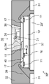
- 부식성 환경에서 부식성 구성요소에 의해 부식될 수 있는 물질의 적어도 하나의 제 1 본드패드(12)를 포함하는 처리 디바이스(10')와,
- 제 1 내부식성 물질로 구성될 수 있고, 및/또는 제 1 내부식성 물질로 덮일 수 있는, 적어도 하나의 제 2 본드패드(21, 21')를 포함하는 센서 디바이스(20, 20')와,
- 상기 처리 디바이스의 적어도 하나의 제 1 본드패드와, 상기 센서 디바이스의 적어도 하나의 제 2 본드패드 사이의 신호 연결을 위한 적어도 하나의 본딩 와이어(34)를 포함하되,
상기 처리 디바이스(10')는 제 2 내부식성 물질(32)에 의해 부분적으로 오버몰딩되고, 상기 제 2 내부식성 물질(32) 내 공동(36)에 부분적으로 노출되며, 상기 센서 디바이스(20, 20')는 상기 공동(36) 내에 존재하고,
제 2 내부식성 물질(32)이 적어도 하나의 제 1 본드패드(12)를 덮는 동안 상기 처리 디바이스(10')와 센서 디바이스(20, 20') 사이의 신호 연결이 공동(36) 내에서 물리적으로 이루어지도록 재분배층(18)이 제공된다.
Description
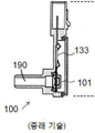
도 3은 종래 기술의 압력 센서 조립체에서 도 1의 압력 센서가 별도의 처리 보드에 어떻게 연결되는지를 더 상세히 보여준다.
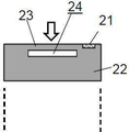
도 4 및 도 5는 본 발명의 실시예에 사용될 수 있는 일례의 별도의 절대 압력 센서의 개략적 측면도 및 평면도이지만, 본 발명은 (가령, 정사각형 단면 및 4개의 본드 패드를 가진) 이러한 구체적 예에 제한되지 않으며, 다른 절대 압력 센서도 또한 사용될 수 있다.
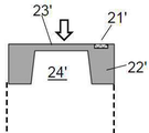
도 6 및 도 7은 본 발명의 실시예에 사용될 수 있는 일례의 별도의 상대 또는 차동 압력 센서의 개략적 측면도 및 평면도로서, 본 발명은 (가령, 정사각형 단면 및 4개의 본드패드를 가진) 이러한 구체적 예에 제한되지 않으며 다른 상대 압력 센서 또한 사용될 수 있다.
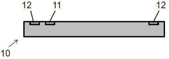
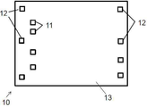
도 8 및 도 9는 본 발명의 실시예에 사용될 수 있는 알루미늄 또는 구리 패드를 가진 일례의 처리 디바이스(가령, CMOS 칩)의 개략적 측면도 및 평면도로서, 본 발명은 (가령, 상단에 11개의 접촉부를 가진) 이러한 구체적 예에 제한되지 않으며 다른 처리 디바이스 또한 사용될 수 있다.
도 10 및 도 11은 도 8 및 도 9에 도시되는 것과 유사한 처리 디바이스의 측면도 및 평면도로서, 상기 처리 디바이스의 알루미늄 또는 구리 패드의 적어도 일부분 위에 오버패드 금속부(OverPad Metallization: "OPM")이 추가되었다. 도 10 및 도 11에서, 모든 패드들은 상단에 OPM을 가진다. OPM을 가진 이러한 처리 디바이스는 본 발명의 실시예에 사용될 수 있다.
도 12는 도 5 및 도 6에 도시되는 것 또는 도 6 및 도 7에 도시되는 것과 유사한 센서 디바이스와, 도 11에 도시된 것과 유사한 OPM을 가진 처리 디바이스를 포함하는 본 발명의 실시예에 따른 센서 조립체의 평면도다. 처리 디바이스는 기판, 가령, 리드프레임 위에 장착된다. 센서 디바이스는 처리 디바이스 위에 장착된다.
도 13은 도 12에 도시되는 것과 유사한 센서 조립체의 측면도로서, 일부 패드들이 예시 용도로 시프트되어 있다.
도 14는 도 12에 도시되는 센서 조립체의 일 변형예의 평면도를 도시한다. 처리 디바이스가 리드 프레임 위에 장착된다. 센서 디바이스 또한, 처리 디바이스에 인접한 위치에서 리드 프레임 위에 장착된다.
도 15는 도 14에 도시되는 것과 유사한 센서 조립체의 측면도를 도시한다(일부 패드는 예시 용도로 시프트됨).
도 16은 오버패드 금속부 위에 추가 부동태층을 가진, 도 113에 도시된 것과 유사한 센서 조립체의 측면도다.
도 17은 본 발명의 일 실시예에 따른 센서 조립체 제조 방법을 도시한다.
도 18은 도 17의 단계들 중 하나를 더 상세히 도시한다.
도면은 단지 개략적이며 비제한적이다. 도면들에서, 일부 구성 요소들의 크기는 과장 될 수 있으며, 설명의 목적으로 일정 규모로 그려지지 않을 수 있다. 청구 범위 내의 임의의 참조 부호는 범위를 제한하는 것으로 해석되어서는 안된다. 상이한 도면에서, 동일한 참조 부호는 동일하거나 유사한 요소를 나타낸다.
Claims (17)
- 부식성 환경에 사용하기 위한 반도체 센서 조립체(30, 30', 30")에 있어서, 상기 센서 조립체(30, 30', 30")는,
- 부식성 환경의 부식성 성분에 의해 부식될 수 있는 물질의 적어도 하나의 제 1 본드패드(12)를 포함하는 처리 디바이스(10')와,
- 제 1 내부식성 물질로 구성되거나 제 1 내부식성 물질로 덮일 수 있는 적어도 하나의 제 2 본드패드(21, 21')를 포함하는 센서 디바이스(20, 20')와,
- 상기 처리 디바이스의 적어도 하나의 제 1 본드패드와, 상기 센서 디바이스의 적어도 하나의 제 2 본드패드 사이를 신호 연결하기 위한 적어도 하나의 본딩 와이어(34)를 포함하되,
상기 처리 디바이스(10')는 제 2 내부식성 물질(32)에 의해 부분적으로 오버몰딩되고, 상기 제 2 내부식성 물질(32) 내 공동(36)에 부분적으로 노출되며, 상기 센서 디바이스(20, 20')는 상기 공동(36) 내에 존재하고,
제 2 내부식성 물질(32)이 적어도 하나의 제 1 본드패드(12)를 덮을 때, 상기 처리 디바이스(10')와 센서 디바이스(20, 20') 간의 신호 연결이 공동(36) 내에서 물리적으로 이루어지도록 재분배층(18)이 제공되는
반도체 센서 조립체. - 제 1 항에 있어서,
상기 재분배층(18)은 오버패드 금속부를 포함하는
반도체 센서 조립체. - 제 2 항에 있어서,
상기 오버패드 금속부는 제 3 내부식성 물질로 구성되고, 상기 오버패드 금속부(18)는 근위부(18a) 및 원위부(18c)를 포함하는 형상을 가지며, 상기 원위부(18c)는 상기 근위부(18a)로부터 특정 거리(L2)에 위치하고 중간부(18b)를 통해 상기 근위부(18a)에 연결되며, 상기 근위부(18a)는 상기 적어도 하나의 제 1 본드패드(12)를 덮는 형상을 가진
반도체 센서 조립체. - 제 3 항에 있어서,
상기 본딩 와이어는 상기 오버패드 금속부(18)의 원위부(18c)에 연결되는 제 1 단부와, 상기 센서 디바이스(20, 20')의 적어도 하나의 제 2 본드패드(21, 21')에 연결되는 제 2 단부를 가지며, 상기 본딩 와이어(34)는 제 4 내부식성 물질로 구성되는
반도체 센서 조립체. - 제 1 항에 있어서,
상기 제 1 내부식성 물질, 제 3 내부식성 물질, 제 4 내부식성 물질 중 적어도 하나는
귀금속(noble metal),
순수 금,
순수 백금,
금과 백금으로만 이루어진 믹스처,
Au 또는 Pt를 함유한 합금
중 적어도 하나로부터 선택되는
반도체 센서 조립체. - 제 1 항 내지 제 5 항 중 어느 한 항에 있어서,
상기 센서 디바이스(20, 20')는 기판(33') 위에 장착되고 상기 처리 디바이스(10')에 인접하여 위치하는
반도체 센서 조립체. - 제 1 항에 있어서,
상기 센서 디바이스(20, 20')가 처리 디바이스(10') 위에 위치하는
반도체 센서 조립체. - 제 1 항에 있어서,
상기 재분배층(18) 위에 부동태층(40)을 더 포함하는
반도체 센서 조립체. - 제 1 항에 있어서,
상기 센서 디바이스(20, 20') 위에 도포되는 겔을 더 포함하는
반도체 센서 조립체. - 제 1 항에 있어서,
기판을 포함하며,
상기 기판(33, 33', 33")은 리드 프레임인
반도체 센서 조립체. - 제 1 항에 있어서,
상기 처리 디바이스(10')는 제 2 본딩 와이어(35)를 통해 기판(33, 33', 33")에 연결되는 제 3 본드패드(11)를 더 포함하며, 상기 제 2 본딩 와이어(35)는 상기 제 2 내부식성 물질(32)에 의해 또한 캡슐화되는
반도체 센서 조립체. - 제 1 항에 있어서,
상기 처리 디바이스(10')는 CMOS 칩이고, 상기 센서 디바이스는 상이한 기술로 제조되는
반도체 센서 조립체. - 제 12 항에 있어서,
상기 CMOS 칩은 마이크로프로세서 및 비휘발성 메모리를 포함하는
반도체 센서 조립체. - 제 1 항에 있어서,
5mm x 10mm x 8mm 보다 작은 외측 치수를 가진
반도체 센서 조립체. - 제 1 항에 있어서,
상기 센서 디바이스(20, 20')는 절대 압력 센서 또는 차동 압력 센서 또는 적외선 센서인
반도체 센서 조립체. - 제 15 항에 있어서,
상기 반도체 센서 조립체가 자동차 엔진의 배기 가스의 압력 및 조성 중 적어도 하나를 측정하는데 사용되는
반도체 센서 조립체. - 반도체 센서 조립체(30, 30', 30")의 제조 방법에 있어서,
- 부식성 환경의 부식성 성분에 의해 부식될 수 있는 물질의 적어도 하나의 제 1 본드패드(12)를 포함하는 처리 디바이스(10')를 제공하는 단계와,
- 제 1 내부식성 물질로 구성되거나 제 1 내부식성 물질로 덮일 수 있는 적어도 하나의 제 2 본드패드(21, 21')를 포함하는 센서 디바이스(20, 20')를 제공하는 단계와,
- 적어도 하나의 본딩 와이어(34)를 이용하여 상기 처리 디바이스의 적어도 하나의 제 1 본드패드와, 상기 센서 디바이스의 적어도 하나의 제 2 본드패드 사이를 신호 연결하는 단계와,
- 상기 처리 디바이스(10')를 제 2 내부식성 물질(32)에 의해 부분적으로 오버몰딩하는 단계 - 상기 처리 디바이스(10')는 상기 제 2 내부식성 물질(32) 내 공동(36)에 부분적으로 노출됨 - 와,
- 상기 센서 디바이스(20, 20')를 상기 공동(36) 내에 장착하는 단계와,
- 처리 디바이스를 부분적으로 오버몰딩하기 전에, 제 2 내부식성 물질(32)이 적어도 하나의 제 1 본드패드(12)를 덮을 때, 상기 처리 디바이스(10')와 센서 디바이스(20, 20') 간의 신호 연결이 공동(36) 내에서 물리적으로 이루어지도록 재분배층(18)을 제공하는 단계를 포함하는
반도체 센서 조립체 제조 방법.
Applications Claiming Priority (2)
| Application Number | Priority Date | Filing Date | Title |
|---|---|---|---|
| EP16175422.1 | 2016-06-21 | ||
| EP16175422.1A EP3260833B1 (en) | 2016-06-21 | 2016-06-21 | Semiconductor sensor assembly for harsh media application |
Publications (1)
| Publication Number | Publication Date |
|---|---|
| KR20170143461A true KR20170143461A (ko) | 2017-12-29 |
Family
ID=56148259
Family Applications (1)
| Application Number | Title | Priority Date | Filing Date |
|---|---|---|---|
| KR1020170078346A Ceased KR20170143461A (ko) | 2016-06-21 | 2017-06-21 | 가혹 환경 반도체 센서 조립체 |
Country Status (5)
| Country | Link |
|---|---|
| US (1) | US10006822B2 (ko) |
| EP (1) | EP3260833B1 (ko) |
| JP (1) | JP2018032846A (ko) |
| KR (1) | KR20170143461A (ko) |
| CN (1) | CN107525620B (ko) |
Families Citing this family (9)
| Publication number | Priority date | Publication date | Assignee | Title |
|---|---|---|---|---|
| EP3211394B1 (en) * | 2016-02-29 | 2021-03-31 | Melexis Technologies NV | Semiconductor pressure sensor for harsh media application |
| EP3260833B1 (en) * | 2016-06-21 | 2021-10-27 | Melexis Technologies NV | Semiconductor sensor assembly for harsh media application |
| US20190206752A1 (en) | 2017-12-29 | 2019-07-04 | Texas Instruments Incorporated | Integrated circuit packages with cavities and methods of manufacturing the same |
| US11543466B2 (en) * | 2018-03-24 | 2023-01-03 | Melexis Technologies Sa | Magnetic sensor component and assembly |
| DE102018222781A1 (de) * | 2018-12-21 | 2020-06-25 | Robert Bosch Gmbh | Drucksensoranordnung |
| CN209326840U (zh) | 2018-12-27 | 2019-08-30 | 热敏碟公司 | 压力传感器及压力变送器 |
| US11545404B2 (en) * | 2020-05-06 | 2023-01-03 | Qualcomm Incorporated | III-V compound semiconductor dies with stress-treated inactive surfaces to avoid packaging-induced fractures, and related methods |
| EP4390355B1 (en) * | 2022-12-23 | 2026-04-08 | Melexis Technologies NV | Protection of sensing element during moulding |
| CN118376665A (zh) * | 2024-06-25 | 2024-07-23 | 苏州烯晶半导体科技有限公司 | 一种监测氢氟酸中ph值的传感器及其制备方法 |
Family Cites Families (15)
| Publication number | Priority date | Publication date | Assignee | Title |
|---|---|---|---|---|
| JPS5217780A (en) | 1975-07-04 | 1977-02-09 | Hitachi Ltd | Pressure convertor with semi-conductor elements |
| US5438876A (en) * | 1993-08-05 | 1995-08-08 | The Foxboro Company | Modular diaphragm pressure sensor with peripheral mounted electrical terminals |
| JPH1096743A (ja) * | 1996-09-25 | 1998-04-14 | Mitsubishi Electric Corp | 半導体センサ及びその製造方法 |
| CN2575640Y (zh) * | 2002-07-25 | 2003-09-24 | 唐铭崇 | 隔膜式压力表 |
| DE102005024215A1 (de) * | 2004-06-03 | 2005-12-22 | Denso Corp., Kariya | Drucksensor |
| US20070052047A1 (en) | 2005-09-01 | 2007-03-08 | Costas Hadjiloucas | Metal contact systems for semiconductor-based pressure sensors exposed to harsh chemical and thermal environments |
| EP1947439B1 (en) | 2005-11-01 | 2012-02-08 | Hitachi, Ltd. | Semiconductor pressure sensor |
| US8237537B2 (en) * | 2006-06-15 | 2012-08-07 | Kulite Semiconductor Products, Inc. | Corrosion-resistant high temperature pressure transducer employing a metal diaphragm |
| JP2008107183A (ja) * | 2006-10-25 | 2008-05-08 | Denso Corp | 半導体装置 |
| US8148808B2 (en) * | 2007-08-13 | 2012-04-03 | Lv Sensors, Inc. | Partitioning of electronic packages |
| US7992441B2 (en) * | 2008-07-31 | 2011-08-09 | Sensata Technologies, Inc. | Pressure sensor for measuring pressure in a medium |
| DE102009047352A1 (de) | 2009-12-01 | 2011-06-09 | Robert Bosch Gmbh | Schichtaufbau zu elektrischen Kontaktierung von Halbleiterbauelementen |
| JP6317956B2 (ja) * | 2014-03-05 | 2018-04-25 | 株式会社フジクラ | 圧力センサ、及び圧力センサの製造方法 |
| CN105181189B (zh) * | 2015-10-23 | 2018-05-29 | 南京信息工程大学 | 基于巨压阻特性的硅纳米线压力传感器及其封装结构 |
| EP3260833B1 (en) * | 2016-06-21 | 2021-10-27 | Melexis Technologies NV | Semiconductor sensor assembly for harsh media application |
-
2016
- 2016-06-21 EP EP16175422.1A patent/EP3260833B1/en active Active
-
2017
- 2017-06-20 JP JP2017120532A patent/JP2018032846A/ja active Pending
- 2017-06-21 CN CN201710475788.5A patent/CN107525620B/zh active Active
- 2017-06-21 KR KR1020170078346A patent/KR20170143461A/ko not_active Ceased
- 2017-06-21 US US15/628,758 patent/US10006822B2/en active Active
Also Published As
| Publication number | Publication date |
|---|---|
| EP3260833B1 (en) | 2021-10-27 |
| CN107525620B (zh) | 2021-11-09 |
| US10006822B2 (en) | 2018-06-26 |
| JP2018032846A (ja) | 2018-03-01 |
| EP3260833A1 (en) | 2017-12-27 |
| US20170363492A1 (en) | 2017-12-21 |
| CN107525620A (zh) | 2017-12-29 |
Similar Documents
| Publication | Publication Date | Title |
|---|---|---|
| US10006822B2 (en) | Semiconductor sensor assembly for harsh media application | |
| US10308502B2 (en) | Semiconductor pressure sensor for harsh media application | |
| US7793550B2 (en) | Sensor device including two sensors embedded in a mold material | |
| AU2009307832B2 (en) | Integrated sensor including sensing and processing die mounted on opposite sides of package substrate | |
| US8969978B2 (en) | TMAP sensor systems and methods for manufacturing those | |
| CN1739014B (zh) | 半导体压力传感器及其制造方法 | |
| EP1947439B1 (en) | Semiconductor pressure sensor | |
| US7549344B2 (en) | Pressure sensor package and electronic part | |
| US20150090030A1 (en) | Transducer arrangement comprising a transducer die and method of covering a transducer die | |
| EP2230507A1 (en) | Humidity or gas sensor | |
| US8264074B2 (en) | Device for use as dual-sided sensor package | |
| US20050269654A1 (en) | Pressure sensor | |
| US20050034526A1 (en) | Semiconductor sensor and method of plating semiconductor devices | |
| US7745916B2 (en) | Module comprising polymer-containing electrical connecting element | |
| CN107490337B (zh) | 应变检测器及其制造方法 | |
| JP5815624B2 (ja) | 防水型圧力センサ | |
| US20110127674A1 (en) | Layer structure for electrical contacting of semiconductor components | |
| US10190925B2 (en) | Low cost overmolded leadframe force sensor with multiple mounting positions | |
| JP2021015936A (ja) | 電子部品パッケージ | |
| JP4207848B2 (ja) | 圧力センサ | |
| CN121521175A (zh) | 多传感器芯片的封装 | |
| CN104810329A (zh) | 传感器封装及其制造方法 | |
| CN110023721A (zh) | 集成电路传感器封装及其制造方法 |
Legal Events
| Date | Code | Title | Description |
|---|---|---|---|
| E13-X000 | Pre-grant limitation requested |
St.27 status event code: A-2-3-E10-E13-lim-X000 |
|
| PA0109 | Patent application |
St.27 status event code: A-0-1-A10-A12-nap-PA0109 |
|
| PG1501 | Laying open of application |
St.27 status event code: A-1-1-Q10-Q12-nap-PG1501 |
|
| A201 | Request for examination | ||
| PA0201 | Request for examination |
St.27 status event code: A-1-2-D10-D11-exm-PA0201 |
|
| E902 | Notification of reason for refusal | ||
| PE0902 | Notice of grounds for rejection |
St.27 status event code: A-1-2-D10-D21-exm-PE0902 |
|
| E601 | Decision to refuse application | ||
| PE0601 | Decision on rejection of patent |
St.27 status event code: N-2-6-B10-B15-exm-PE0601 |
|
| R18-X000 | Changes to party contact information recorded |
St.27 status event code: A-3-3-R10-R18-oth-X000 |
|
| P22-X000 | Classification modified |
St.27 status event code: A-2-2-P10-P22-nap-X000 |
|
| P22-X000 | Classification modified |
St.27 status event code: A-2-2-P10-P22-nap-X000 |
|
| P22-X000 | Classification modified |
St.27 status event code: A-2-2-P10-P22-nap-X000 |