KR20180062402A - 핀홀 어레이를 사용하는 물체의 공초점형 이미징 - Google Patents
핀홀 어레이를 사용하는 물체의 공초점형 이미징 Download PDFInfo
- Publication number
- KR20180062402A KR20180062402A KR1020170161560A KR20170161560A KR20180062402A KR 20180062402 A KR20180062402 A KR 20180062402A KR 1020170161560 A KR1020170161560 A KR 1020170161560A KR 20170161560 A KR20170161560 A KR 20170161560A KR 20180062402 A KR20180062402 A KR 20180062402A
- Authority
- KR
- South Korea
- Prior art keywords
- pinhole array
- pinhole
- imaging device
- array
- pinholes
- Prior art date
- Legal status (The legal status is an assumption and is not a legal conclusion. Google has not performed a legal analysis and makes no representation as to the accuracy of the status listed.)
- Granted
Links
Images

Classifications
-
- G—PHYSICS
- G01—MEASURING; TESTING
- G01N—INVESTIGATING OR ANALYSING MATERIALS BY DETERMINING THEIR CHEMICAL OR PHYSICAL PROPERTIES
- G01N21/00—Investigating or analysing materials by the use of optical means, i.e. using sub-millimetre waves, infrared, visible or ultraviolet light
- G01N21/84—Systems specially adapted for particular applications
- G01N21/88—Investigating the presence of flaws or contamination
- G01N21/8806—Specially adapted optical and illumination features
-
- G—PHYSICS
- G02—OPTICS
- G02B—OPTICAL ELEMENTS, SYSTEMS OR APPARATUS
- G02B21/00—Microscopes
- G02B21/0004—Microscopes specially adapted for specific applications
- G02B21/002—Scanning microscopes
- G02B21/0024—Confocal scanning microscopes (CSOMs) or confocal "macroscopes"; Accessories which are not restricted to use with CSOMs, e.g. sample holders
- G02B21/0036—Scanning details, e.g. scanning stages
- G02B21/0044—Scanning details, e.g. scanning stages moving apertures, e.g. Nipkow disks, rotating lens arrays
-
- G—PHYSICS
- G01—MEASURING; TESTING
- G01N—INVESTIGATING OR ANALYSING MATERIALS BY DETERMINING THEIR CHEMICAL OR PHYSICAL PROPERTIES
- G01N21/00—Investigating or analysing materials by the use of optical means, i.e. using sub-millimetre waves, infrared, visible or ultraviolet light
- G01N21/01—Arrangements or apparatus for facilitating the optical investigation
-
- G—PHYSICS
- G01—MEASURING; TESTING
- G01N—INVESTIGATING OR ANALYSING MATERIALS BY DETERMINING THEIR CHEMICAL OR PHYSICAL PROPERTIES
- G01N21/00—Investigating or analysing materials by the use of optical means, i.e. using sub-millimetre waves, infrared, visible or ultraviolet light
- G01N21/17—Systems in which incident light is modified in accordance with the properties of the material investigated
- G01N21/21—Polarisation-affecting properties
-
- G—PHYSICS
- G01—MEASURING; TESTING
- G01N—INVESTIGATING OR ANALYSING MATERIALS BY DETERMINING THEIR CHEMICAL OR PHYSICAL PROPERTIES
- G01N21/00—Investigating or analysing materials by the use of optical means, i.e. using sub-millimetre waves, infrared, visible or ultraviolet light
- G01N21/84—Systems specially adapted for particular applications
- G01N21/88—Investigating the presence of flaws or contamination
- G01N21/95—Investigating the presence of flaws or contamination characterised by the material or shape of the object to be examined
- G01N21/956—Inspecting patterns on the surface of objects
-
- G—PHYSICS
- G02—OPTICS
- G02B—OPTICAL ELEMENTS, SYSTEMS OR APPARATUS
- G02B21/00—Microscopes
- G02B21/0004—Microscopes specially adapted for specific applications
- G02B21/0016—Technical microscopes, e.g. for inspection or measuring in industrial production processes
-
- G—PHYSICS
- G02—OPTICS
- G02B—OPTICAL ELEMENTS, SYSTEMS OR APPARATUS
- G02B21/00—Microscopes
- G02B21/0004—Microscopes specially adapted for specific applications
- G02B21/002—Scanning microscopes
- G02B21/0024—Confocal scanning microscopes (CSOMs) or confocal "macroscopes"; Accessories which are not restricted to use with CSOMs, e.g. sample holders
- G02B21/0028—Confocal scanning microscopes (CSOMs) or confocal "macroscopes"; Accessories which are not restricted to use with CSOMs, e.g. sample holders specially adapted for specific applications, e.g. for endoscopes, ophthalmoscopes, attachments to conventional microscopes
-
- G—PHYSICS
- G02—OPTICS
- G02B—OPTICAL ELEMENTS, SYSTEMS OR APPARATUS
- G02B21/00—Microscopes
- G02B21/0004—Microscopes specially adapted for specific applications
- G02B21/002—Scanning microscopes
- G02B21/0024—Confocal scanning microscopes (CSOMs) or confocal "macroscopes"; Accessories which are not restricted to use with CSOMs, e.g. sample holders
- G02B21/0032—Optical details of illumination, e.g. light-sources, pinholes, beam splitters, slits, fibers
-
- H—ELECTRICITY
- H04—ELECTRIC COMMUNICATION TECHNIQUE
- H04N—PICTORIAL COMMUNICATION, e.g. TELEVISION
- H04N25/00—Circuitry of solid-state image sensors [SSIS]; Control thereof
- H04N25/70—SSIS architectures; Circuits associated therewith
- H04N25/71—Charge-coupled device [CCD] sensors; Charge-transfer registers specially adapted for CCD sensors
-
- G—PHYSICS
- G01—MEASURING; TESTING
- G01N—INVESTIGATING OR ANALYSING MATERIALS BY DETERMINING THEIR CHEMICAL OR PHYSICAL PROPERTIES
- G01N21/00—Investigating or analysing materials by the use of optical means, i.e. using sub-millimetre waves, infrared, visible or ultraviolet light
- G01N21/84—Systems specially adapted for particular applications
- G01N21/88—Investigating the presence of flaws or contamination
- G01N21/8851—Scan or image signal processing specially adapted therefor, e.g. for scan signal adjustment, for detecting different kinds of defects, for compensating for structures, markings, edges
- G01N2021/8887—Scan or image signal processing specially adapted therefor, e.g. for scan signal adjustment, for detecting different kinds of defects, for compensating for structures, markings, edges based on image processing techniques
Landscapes
- Physics & Mathematics (AREA)
- Analytical Chemistry (AREA)
- General Physics & Mathematics (AREA)
- Chemical & Material Sciences (AREA)
- Optics & Photonics (AREA)
- Health & Medical Sciences (AREA)
- General Health & Medical Sciences (AREA)
- Life Sciences & Earth Sciences (AREA)
- Immunology (AREA)
- Biochemistry (AREA)
- Pathology (AREA)
- Ophthalmology & Optometry (AREA)
- Radiology & Medical Imaging (AREA)
- Surgery (AREA)
- Signal Processing (AREA)
- Multimedia (AREA)
- Engineering & Computer Science (AREA)
- Microscoopes, Condenser (AREA)
- Length Measuring Devices By Optical Means (AREA)
- Image Input (AREA)
- Investigating Materials By The Use Of Optical Means Adapted For Particular Applications (AREA)
Abstract
Description
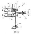
도 1은 물체 표면을 스캔하기 위해 사용되는 종래 기술의 닙코 디스크의 등면도이다.
도 2는 본 발명의 양호한 실시예에 따른 공초점형 검사 장치의 등면도이다.
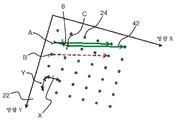
도 3은 도 2에 도시된 공초점형 검사 장치와 함께 사용가능한 핀홀 어레이의 평면도이다.
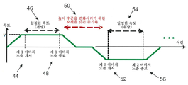
도 4는 핀홀 어레이의 사용과 연계된 예시적인 이미지 캡처 시퀀스를 도시하는 그래프이다.
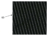
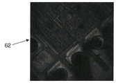
도 5a 및 도 5b는 본 발명의 양호한 실시예에 따른 공초점형 검사 장치에 의해서 각각 얻어진 공초점형 이미지 및 정적 핀홀 어레이의 이미지들이다.


Claims (19)
- 물체를 검사하기 위한 공초점형 이미징 장치에 있어서,
상기 물체를 조명하기 위해 광을 투영하도록 작동되는 광원;
상기 물체 및 이미징 디바이스 사이에 위치한 광 경로를 따라 상기 물체로부터 반사된 광을 수광하기 위한 상기 이미징 디바이스;
상기 물체로부터 반사된 광이 핀홀 어레이를 통과하도록 상기 광 경로를 따라 배치된 복수의 핀홀들을 포함하는 상기 핀홀 어레이; 및
상기 물체의 실질적인 접촉 영역에 대응하는 이미지를 상기 이미징 디바이스 상으로 투과시키기 위한 상기 광 경로를 가로지르는 선형 방향으로 단일축을 따라서 상기 핀홀 어레이를 이동시키기 위한 기구를 포함하는, 공초점형 이미징 장치. - 제 1 항에 있어서,
상기 핀홀 어레이는 상기 광원으로부터 투영된 광이 상기 물체를 조명하기 전에 상기 핀홀 어레이를 통과하도록 배치되는, 공초점형 이미징 장치. - 제 1 항에 있어서,
상기 핀홀 어레이는 매트릭스 배열로 분포된 복수의 핀홀들을 구비한 핀홀 판을 포함하는, 공초점형 이미징 장치. - 제 3 항에 있어서,
상기 매트릭스 배열의 상기 핀홀들은 상기 핀홀 어레이에 의해서 이동한 상기 선형 방향에 대해서 일정각도로 경사지는, 공초점형 이미징 장치. - 제 4 항에 있어서,
상기 각도는 상기 물체의 실질적인 접촉 영역의 전체가 단지 상기 선형 방향으로 상기 핀홀 어레이의 상기 모션을 사용하여 상기 이미징 디바이스 상으로 투과될 수 있도록 선택되는, 공초점형 이미징 장치. - 제 4 항에 있어서,
상기 각도는 상기 물체의 실질적인 접촉 영역의 이미지의 시야의 시야가 상기 선형 방향으로 상기 핀홀 어레이의 모션에 의해서 완전히 채워지도록 선택되는, 공초점형 이미징 장치. - 제 3 항에 있어서,
상기 매트릭스 배열의 제 1 방향(X)으로의 인접 핀홀들 사이의 분리 거리는 상기 제 1 방향과 직각인 제 2 방향(Y)으로의 인접 핀홀들 사이의 분리 거리와 동일한, 공초점형 이미징 장치. - 제 1 항에 있어서,
상기 핀홀 어레이는 각각의 검사 동작에 대해 실질적으로 일정한 속도에서 상기 광 경로에 대한 상기 선형 방향으로 전방 및 후방으로 교대로 이동되도록 구성되는, 공초점형 이미징 장치. - 제 8 항에 있어서,
상기 이미징 디바이스의 이미지 노출은 사전 결정된 이동 거리가 상기 핀홀 어레이에 의해서 도달될 때까지 실질적으로 일정한 속도에서 상기 핀홀 어레이의 이동 중에 작동되는, 공초점형 이미징 장치. - 제 1 항에 있어서,
상기 핀홀 어레이 및 상기 물체 사이에서 상기 광 경로를 따라 배치된 1/4 파장의 파장판 및 크로매틱 요소를 추가로 포함하는, 공초점형 이미징 장치. - 제 1 항에 있어서,
상기 이미징 디바이스는 CCD 카메라를 포함하는, 공초점형 이미징 장치. - 공초점형 이미징 장치를 사용하여 물체를 검사하기 위한 방법에 있어서,
광원으로부터의 광을 상기 물체 상으로 투영함으로써 상기 물체를 조명하는 단계;
상기 물체 및 이미징 디바이스 사이에 위치한 광 경로를 따라 상기 물체로부터 반사된 광을 상기 이미징 디바이스에 의해서 수광하는 단계로서, 상기 물체로부터 반사된 광이 상기 광 경로를 따라 배치된 복수의 핀홀들을 포함하는 핀홀 어레이를 통과하는, 상기 수광 단계; 그리고
상기 물체를 검사하기 위해 상기 물체의 실질적인 접촉 영역에 대응하는 이미지를 상기 이미징 디바이스 상으로 투과시키기 위한 상기 광 경로를 가로지르는 선형 방향으로 단일축을 따라서 상기 핀홀 어레이를 이동시키는 단계를 포함하는, 물체 검사 방법. - 제 12 항에 있어서,
상기 핀홀 어레이는 상기 광원으로부터 투영된 광이 상기 물체를 조명하기 전에 상기 핀홀 어레이를 통과하도록 배치되는, 물체 검사 방법. - 제 12 항에 있어서,
상기 핀홀 어레이는 매트릭스 배열로 분포된 복수의 핀홀들을 구비한 핀홀 판을 포함하는, 물체 검사 방법. - 제 14 항에 있어서,
상기 매트릭스 배열의 상기 핀홀들은 상기 핀홀 어레이에 의해서 이동한 상기 선형 방향에 대해서 일정각도로 경사지는, 물체 검사 방법. - 제 15 항에 있어서,
상기 각도는 상기 물체의 실질적인 접촉 영역의 전체가 단지 상기 선형 방향으로 상기 핀홀 어레이의 상기 모션을 사용하여 상기 이미징 디바이스 상으로 투과될 수 있도록 선택될 수 있는, 물체 검사 방법. - 제 12 항에 있어서,
제 1 검사 동작에서 상기 선형 방향으로 전방으로 상기 핀홀 어레이를 이동시키는 단계, 그리고 그 후에 실질적으로 일정한 속도에서 상기 광 경로에 대하여 제 2 검사 동작에서 상기 선형 방향으로 후방으로 상기 핀홀 어레이를 이동시키는 단계를 추가로 포함하는, 물체 검사 방법. - 제 17 항에 있어서,
사전 결정된 이동 거리가 상기 핀홀 어레이에 의해서 도달될 때까지 실질적으로 일정한 속도에서 상기 핀홀 어레이의 이동 중에 상기 이미징 디바이스의 이미지 노출을 작동시키는 단계를 추가로 포함하는, 물체 검사 방법. - 제 12 항에 있어서,
상기 이미징 디바이스는 CCD 카메라를 포함하는, 물체 검사 방법.
Applications Claiming Priority (2)
| Application Number | Priority Date | Filing Date | Title |
|---|---|---|---|
| US15/365,066 | 2016-11-30 | ||
| US15/365,066 US10852519B2 (en) | 2016-11-30 | 2016-11-30 | Confocal imaging of an object utilising a pinhole array |
Publications (2)
| Publication Number | Publication Date |
|---|---|
| KR20180062402A true KR20180062402A (ko) | 2018-06-08 |
| KR102086992B1 KR102086992B1 (ko) | 2020-03-10 |
Family
ID=62193203
Family Applications (1)
| Application Number | Title | Priority Date | Filing Date |
|---|---|---|---|
| KR1020170161560A Active KR102086992B1 (ko) | 2016-11-30 | 2017-11-29 | 핀홀 어레이를 사용하는 물체의 공초점형 이미징 |
Country Status (6)
| Country | Link |
|---|---|
| US (1) | US10852519B2 (ko) |
| JP (1) | JP6606159B2 (ko) |
| KR (1) | KR102086992B1 (ko) |
| CN (1) | CN108120676B (ko) |
| MY (1) | MY189539A (ko) |
| TW (1) | TWI662637B (ko) |
Cited By (3)
| Publication number | Priority date | Publication date | Assignee | Title |
|---|---|---|---|---|
| KR20210151474A (ko) * | 2020-06-05 | 2021-12-14 | 한국과학기술원 | 마이크로렌즈 어레이를 이용한 초박형 카메라 장치 그리고 이의 다기능 이미징 방법 |
| KR102617147B1 (ko) * | 2023-07-14 | 2023-12-27 | (주)오로스 테크놀로지 | 오버레이 계측 장치 및 오버레이 계측 장치의 교정방법 |
| KR102655300B1 (ko) * | 2023-08-11 | 2024-04-05 | (주)오로스 테크놀로지 | 오버레이 계측 장치의 보정 방법 및 오버레이 계측 장치의 보정 시스템 |
Families Citing this family (4)
| Publication number | Priority date | Publication date | Assignee | Title |
|---|---|---|---|---|
| CN111307068B (zh) * | 2020-04-02 | 2025-02-25 | 元素光电智能科技(苏州)有限公司 | 光学三维测量系统 |
| US20240241056A1 (en) * | 2021-08-30 | 2024-07-18 | Nanostring Technologies, Inc. | Methods, systems and apparatus for a multi-spectral structured illumination microscope |
| US12202069B2 (en) | 2022-04-11 | 2025-01-21 | Salasoft Inc | System and method for calibrating laser marking and cutting systems |
| CN115665563B (zh) * | 2022-12-14 | 2023-06-27 | 深圳市中图仪器股份有限公司 | 光学测量系统及基于光学测量系统的成像方法 |
Citations (5)
| Publication number | Priority date | Publication date | Assignee | Title |
|---|---|---|---|---|
| JPH10326587A (ja) * | 1997-04-07 | 1998-12-08 | Carl Zeiss:Fa | 電動スキャニングテーブル付き共焦点顕微鏡 |
| JP2006337103A (ja) * | 2005-05-31 | 2006-12-14 | Sunx Ltd | 光学測定装置 |
| JP2009526216A (ja) * | 2006-02-08 | 2009-07-16 | シロナ・デンタル・システムズ・ゲゼルシャフト・ミット・ベシュレンクテル・ハフツング | クロマティック共焦点三次元計測技術のための迅速かつ強力な方法および装置 |
| KR20120056948A (ko) * | 2010-11-26 | 2012-06-05 | 주식회사 나노프로텍 | 마이크로 렌즈 어레이를 이용한 공초점 측정 장치 |
| JP2014142183A (ja) * | 2013-01-22 | 2014-08-07 | Takaoka Electric Mfg Co Ltd | 共焦点スキャナおよびそれを用いた光学的計測装置 |
Family Cites Families (17)
| Publication number | Priority date | Publication date | Assignee | Title |
|---|---|---|---|---|
| US5001409A (en) * | 1987-10-09 | 1991-03-19 | Hitachi, Ltd. | Surface metrological apparatus |
| DE10350918B3 (de) * | 2003-10-31 | 2005-04-14 | Evotec Technologies Gmbh | Vorrichtung und Verfahren zur Messung der Transmission eines Objekts |
| GB2419777B (en) * | 2004-10-29 | 2010-02-10 | Hewlett Packard Development Co | Power transfer for transponder devices |
| CN101384293B (zh) * | 2006-03-06 | 2013-04-24 | 泰尔茂株式会社 | 导丝 |
| US8214007B2 (en) * | 2006-11-01 | 2012-07-03 | Welch Allyn, Inc. | Body worn physiological sensor device having a disposable electrode module |
| JP4452815B2 (ja) * | 2007-07-31 | 2010-04-21 | レーザーテック株式会社 | 深さ測定装置 |
| JP5484879B2 (ja) * | 2009-12-11 | 2014-05-07 | オリンパス株式会社 | 超解像顕微鏡 |
| US9606343B2 (en) * | 2011-05-06 | 2017-03-28 | Visitech International Ltd | Enhancing spatial resolution utilizing multibeam confocal scanning systems |
| GB201107556D0 (en) * | 2011-05-06 | 2011-06-22 | Sheblee Jafer | Spatial resolution enhancements in multibeam confocal scanning systems |
| JP5527625B2 (ja) * | 2011-11-22 | 2014-06-18 | 横河電機株式会社 | 顕微鏡装置 |
| EP2967325A4 (en) * | 2013-03-15 | 2017-03-08 | NeuroVision Imaging LLC | System and method for rejecting afocal light collected from an in vivo human retina |
| JP6500774B2 (ja) * | 2013-03-29 | 2019-04-17 | ソニー株式会社 | レーザ走査型内視鏡装置 |
| US9067278B2 (en) * | 2013-03-29 | 2015-06-30 | Photon Automation, Inc. | Pulse spread laser |
| AU2015243218B2 (en) * | 2014-04-11 | 2019-03-21 | Covidien Lp | Tagged surgical instruments and methods therefor |
| CN103944225B (zh) * | 2014-04-16 | 2017-04-26 | 华为技术有限公司 | 电池智能管理方法、电池智能管理装置及电池 |
| US10352860B2 (en) * | 2014-04-24 | 2019-07-16 | Bruker Nano, Inc. | Super resolution microscopy |
| JP6622723B2 (ja) * | 2015-01-30 | 2019-12-18 | 国立研究開発法人科学技術振興機構 | 多焦点分光計測装置、及び多焦点分光計測装置用光学系 |
-
2016
- 2016-11-30 US US15/365,066 patent/US10852519B2/en active Active
-
2017
- 2017-01-13 CN CN201710025272.0A patent/CN108120676B/zh active Active
- 2017-11-15 MY MYPI2017001672A patent/MY189539A/en unknown
- 2017-11-17 TW TW106139806A patent/TWI662637B/zh active
- 2017-11-29 KR KR1020170161560A patent/KR102086992B1/ko active Active
- 2017-11-29 JP JP2017228855A patent/JP6606159B2/ja active Active
Patent Citations (5)
| Publication number | Priority date | Publication date | Assignee | Title |
|---|---|---|---|---|
| JPH10326587A (ja) * | 1997-04-07 | 1998-12-08 | Carl Zeiss:Fa | 電動スキャニングテーブル付き共焦点顕微鏡 |
| JP2006337103A (ja) * | 2005-05-31 | 2006-12-14 | Sunx Ltd | 光学測定装置 |
| JP2009526216A (ja) * | 2006-02-08 | 2009-07-16 | シロナ・デンタル・システムズ・ゲゼルシャフト・ミット・ベシュレンクテル・ハフツング | クロマティック共焦点三次元計測技術のための迅速かつ強力な方法および装置 |
| KR20120056948A (ko) * | 2010-11-26 | 2012-06-05 | 주식회사 나노프로텍 | 마이크로 렌즈 어레이를 이용한 공초점 측정 장치 |
| JP2014142183A (ja) * | 2013-01-22 | 2014-08-07 | Takaoka Electric Mfg Co Ltd | 共焦点スキャナおよびそれを用いた光学的計測装置 |
Cited By (5)
| Publication number | Priority date | Publication date | Assignee | Title |
|---|---|---|---|---|
| KR20210151474A (ko) * | 2020-06-05 | 2021-12-14 | 한국과학기술원 | 마이크로렌즈 어레이를 이용한 초박형 카메라 장치 그리고 이의 다기능 이미징 방법 |
| US11818473B2 (en) | 2020-06-05 | 2023-11-14 | Korea Advanced Institute Of Science And Technology | Ultrathin camera device using microlens array, and multi-functional imaging method using the same |
| KR102617147B1 (ko) * | 2023-07-14 | 2023-12-27 | (주)오로스 테크놀로지 | 오버레이 계측 장치 및 오버레이 계측 장치의 교정방법 |
| KR102655300B1 (ko) * | 2023-08-11 | 2024-04-05 | (주)오로스 테크놀로지 | 오버레이 계측 장치의 보정 방법 및 오버레이 계측 장치의 보정 시스템 |
| WO2025037806A1 (ko) * | 2023-08-11 | 2025-02-20 | (주) 오로스테크놀로지 | 오버레이 계측 장치의 보정 방법 및 오버레이 계측 장치의 보정 시스템 |
Also Published As
| Publication number | Publication date |
|---|---|
| TW201834099A (zh) | 2018-09-16 |
| KR102086992B1 (ko) | 2020-03-10 |
| US20180149848A1 (en) | 2018-05-31 |
| JP6606159B2 (ja) | 2019-11-13 |
| US10852519B2 (en) | 2020-12-01 |
| CN108120676A (zh) | 2018-06-05 |
| JP2018092166A (ja) | 2018-06-14 |
| TWI662637B (zh) | 2019-06-11 |
| CN108120676B (zh) | 2020-08-18 |
| MY189539A (en) | 2022-02-16 |
Similar Documents
| Publication | Publication Date | Title |
|---|---|---|
| KR102086992B1 (ko) | 핀홀 어레이를 사용하는 물체의 공초점형 이미징 | |
| KR100474100B1 (ko) | 공초점 현미경 및 이것을 이용한 높이 측정방법 | |
| JP3440465B2 (ja) | マルチスリット走査撮像装置 | |
| US8610902B2 (en) | Apparatus and method for inspecting an object with increased depth of field | |
| JP5376076B1 (ja) | 共焦点スキャナおよびそれを用いた光学的計測装置 | |
| TW201407128A (zh) | 彩色共焦掃描裝置 | |
| JP2000275027A (ja) | スリット共焦点顕微鏡とそれを用いた表面形状計測装置 | |
| CN103180769B (zh) | 显微镜、图像获取装置和图像获取系统 | |
| JP4115624B2 (ja) | 3次元形状測定装置 | |
| KR101428864B1 (ko) | 초점 위치 변경 장치 및 이를 이용한 공초점 광학 장치 | |
| JP3509088B2 (ja) | 3次元形状計測用光学装置 | |
| KR100845284B1 (ko) | 두개의 닙코우 디스크를 이용한 공초점 주사 현미경 | |
| JP2006105835A (ja) | 形状測定方法及び形状測定装置 | |
| JP4788968B2 (ja) | 焦点面傾斜型共焦点表面形状計測装置 | |
| KR102814284B1 (ko) | 공초점 센싱 시스템 | |
| JPH0499907A (ja) | 曲率半径の非接触測定方法 | |
| JP4214555B2 (ja) | パターン位置計測装置 | |
| JPH1183755A (ja) | 傷検査装置 | |
| JP2025536783A (ja) | 共焦点眼底検査を実施するためのシステム | |
| CN120028345A (zh) | 一种光学检测装置 | |
| JP2007171817A (ja) | レーザ顕微鏡 | |
| JP2008145162A (ja) | 三次元形状測定装置 | |
| RU2525152C2 (ru) | Способ формирования изображения микрообъекта (варианты) и устройство для его осуществления (варианты) |
Legal Events
| Date | Code | Title | Description |
|---|---|---|---|
| PA0109 | Patent application |
Patent event code: PA01091R01D Comment text: Patent Application Patent event date: 20171129 |
|
| A201 | Request for examination | ||
| PA0201 | Request for examination |
Patent event code: PA02012R01D Patent event date: 20171227 Comment text: Request for Examination of Application Patent event code: PA02011R01I Patent event date: 20171129 Comment text: Patent Application |
|
| PG1501 | Laying open of application | ||
| E902 | Notification of reason for refusal | ||
| PE0902 | Notice of grounds for rejection |
Comment text: Notification of reason for refusal Patent event date: 20190409 Patent event code: PE09021S01D |
|
| E90F | Notification of reason for final refusal | ||
| PE0902 | Notice of grounds for rejection |
Comment text: Final Notice of Reason for Refusal Patent event date: 20190822 Patent event code: PE09021S02D |
|
| E701 | Decision to grant or registration of patent right | ||
| PE0701 | Decision of registration |
Patent event code: PE07011S01D Comment text: Decision to Grant Registration Patent event date: 20200204 |
|
| GRNT | Written decision to grant | ||
| PR0701 | Registration of establishment |
Comment text: Registration of Establishment Patent event date: 20200304 Patent event code: PR07011E01D |
|
| PR1002 | Payment of registration fee |
Payment date: 20200305 End annual number: 3 Start annual number: 1 |
|
| PG1601 | Publication of registration | ||
| PR1001 | Payment of annual fee |
Payment date: 20240222 Start annual number: 5 End annual number: 5 |
|
| PR1001 | Payment of annual fee |
Payment date: 20250218 Start annual number: 6 End annual number: 6 |