KR20180071283A - 콘덴서 및 그의 제조 방법 및 그것을 사용한 무선 통신 장치 - Google Patents
콘덴서 및 그의 제조 방법 및 그것을 사용한 무선 통신 장치 Download PDFInfo
- Publication number
- KR20180071283A KR20180071283A KR1020187012797A KR20187012797A KR20180071283A KR 20180071283 A KR20180071283 A KR 20180071283A KR 1020187012797 A KR1020187012797 A KR 1020187012797A KR 20187012797 A KR20187012797 A KR 20187012797A KR 20180071283 A KR20180071283 A KR 20180071283A
- Authority
- KR
- South Korea
- Prior art keywords
- capacitor
- dielectric layer
- group
- metal
- compound
- Prior art date
- Legal status (The legal status is an assumption and is not a legal conclusion. Google has not performed a legal analysis and makes no representation as to the accuracy of the status listed.)
- Granted
Links
Images



Classifications
-
- H—ELECTRICITY
- H10—SEMICONDUCTOR DEVICES; ELECTRIC SOLID-STATE DEVICES NOT OTHERWISE PROVIDED FOR
- H10D—INORGANIC ELECTRIC SEMICONDUCTOR DEVICES
- H10D1/00—Resistors, capacitors or inductors
- H10D1/60—Capacitors
- H10D1/68—Capacitors having no potential barriers
-
- H—ELECTRICITY
- H01—ELECTRIC ELEMENTS
- H01G—CAPACITORS; CAPACITORS, RECTIFIERS, DETECTORS, SWITCHING DEVICES, LIGHT-SENSITIVE OR TEMPERATURE-SENSITIVE DEVICES OF THE ELECTROLYTIC TYPE
- H01G4/00—Fixed capacitors; Processes of their manufacture
- H01G4/002—Details
- H01G4/018—Dielectrics
- H01G4/06—Solid dielectrics
- H01G4/14—Organic dielectrics
-
- G—PHYSICS
- G06—COMPUTING OR CALCULATING; COUNTING
- G06K—GRAPHICAL DATA READING; PRESENTATION OF DATA; RECORD CARRIERS; HANDLING RECORD CARRIERS
- G06K19/00—Record carriers for use with machines and with at least a part designed to carry digital markings
- G06K19/06—Record carriers for use with machines and with at least a part designed to carry digital markings characterised by the kind of the digital marking, e.g. shape, nature, code
- G06K19/067—Record carriers with conductive marks, printed circuits or semiconductor circuit elements, e.g. credit or identity cards also with resonating or responding marks without active components
- G06K19/07—Record carriers with conductive marks, printed circuits or semiconductor circuit elements, e.g. credit or identity cards also with resonating or responding marks without active components with integrated circuit chips
- G06K19/077—Constructional details, e.g. mounting of circuits in the carrier
-
- G—PHYSICS
- G06—COMPUTING OR CALCULATING; COUNTING
- G06K—GRAPHICAL DATA READING; PRESENTATION OF DATA; RECORD CARRIERS; HANDLING RECORD CARRIERS
- G06K19/00—Record carriers for use with machines and with at least a part designed to carry digital markings
- G06K19/06—Record carriers for use with machines and with at least a part designed to carry digital markings characterised by the kind of the digital marking, e.g. shape, nature, code
- G06K19/067—Record carriers with conductive marks, printed circuits or semiconductor circuit elements, e.g. credit or identity cards also with resonating or responding marks without active components
- G06K19/07—Record carriers with conductive marks, printed circuits or semiconductor circuit elements, e.g. credit or identity cards also with resonating or responding marks without active components with integrated circuit chips
- G06K19/077—Constructional details, e.g. mounting of circuits in the carrier
- G06K19/07749—Constructional details, e.g. mounting of circuits in the carrier the record carrier being capable of non-contact communication, e.g. constructional details of the antenna of a non-contact smart card
- G06K19/0775—Constructional details, e.g. mounting of circuits in the carrier the record carrier being capable of non-contact communication, e.g. constructional details of the antenna of a non-contact smart card arrangements for connecting the integrated circuit to the antenna
-
- H—ELECTRICITY
- H01—ELECTRIC ELEMENTS
- H01G—CAPACITORS; CAPACITORS, RECTIFIERS, DETECTORS, SWITCHING DEVICES, LIGHT-SENSITIVE OR TEMPERATURE-SENSITIVE DEVICES OF THE ELECTROLYTIC TYPE
- H01G4/00—Fixed capacitors; Processes of their manufacture
- H01G4/002—Details
- H01G4/005—Electrodes
- H01G4/008—Selection of materials
-
- H—ELECTRICITY
- H01—ELECTRIC ELEMENTS
- H01G—CAPACITORS; CAPACITORS, RECTIFIERS, DETECTORS, SWITCHING DEVICES, LIGHT-SENSITIVE OR TEMPERATURE-SENSITIVE DEVICES OF THE ELECTROLYTIC TYPE
- H01G4/00—Fixed capacitors; Processes of their manufacture
- H01G4/002—Details
- H01G4/018—Dielectrics
- H01G4/06—Solid dielectrics
- H01G4/08—Inorganic dielectrics
- H01G4/10—Metal-oxide dielectrics
-
- H—ELECTRICITY
- H01—ELECTRIC ELEMENTS
- H01G—CAPACITORS; CAPACITORS, RECTIFIERS, DETECTORS, SWITCHING DEVICES, LIGHT-SENSITIVE OR TEMPERATURE-SENSITIVE DEVICES OF THE ELECTROLYTIC TYPE
- H01G4/00—Fixed capacitors; Processes of their manufacture
- H01G4/002—Details
- H01G4/018—Dielectrics
- H01G4/06—Solid dielectrics
- H01G4/14—Organic dielectrics
- H01G4/18—Organic dielectrics of synthetic material, e.g. derivatives of cellulose
-
- H—ELECTRICITY
- H01—ELECTRIC ELEMENTS
- H01G—CAPACITORS; CAPACITORS, RECTIFIERS, DETECTORS, SWITCHING DEVICES, LIGHT-SENSITIVE OR TEMPERATURE-SENSITIVE DEVICES OF THE ELECTROLYTIC TYPE
- H01G4/00—Fixed capacitors; Processes of their manufacture
- H01G4/002—Details
- H01G4/018—Dielectrics
- H01G4/20—Dielectrics using combinations of dielectrics from more than one of groups H01G4/02 - H01G4/06
- H01G4/206—Dielectrics using combinations of dielectrics from more than one of groups H01G4/02 - H01G4/06 inorganic and synthetic material
-
- H—ELECTRICITY
- H01—ELECTRIC ELEMENTS
- H01G—CAPACITORS; CAPACITORS, RECTIFIERS, DETECTORS, SWITCHING DEVICES, LIGHT-SENSITIVE OR TEMPERATURE-SENSITIVE DEVICES OF THE ELECTROLYTIC TYPE
- H01G4/00—Fixed capacitors; Processes of their manufacture
- H01G4/33—Thin- or thick-film capacitors (thin- or thick-film circuits; capacitors without a potential-jump or surface barrier specially adapted for integrated circuits, details thereof, multistep manufacturing processes therefor)
-
- H—ELECTRICITY
- H01—ELECTRIC ELEMENTS
- H01G—CAPACITORS; CAPACITORS, RECTIFIERS, DETECTORS, SWITCHING DEVICES, LIGHT-SENSITIVE OR TEMPERATURE-SENSITIVE DEVICES OF THE ELECTROLYTIC TYPE
- H01G4/00—Fixed capacitors; Processes of their manufacture
- H01G4/40—Structural combinations of fixed capacitors with other electric elements, the structure mainly consisting of a capacitor, e.g. RC combinations
-
- H—ELECTRICITY
- H10—SEMICONDUCTOR DEVICES; ELECTRIC SOLID-STATE DEVICES NOT OTHERWISE PROVIDED FOR
- H10D—INORGANIC ELECTRIC SEMICONDUCTOR DEVICES
- H10D84/00—Integrated devices formed in or on semiconductor substrates that comprise only semiconducting layers, e.g. on Si wafers or on GaAs-on-Si wafers
- H10D84/80—Integrated devices formed in or on semiconductor substrates that comprise only semiconducting layers, e.g. on Si wafers or on GaAs-on-Si wafers characterised by the integration of at least one component covered by groups H10D12/00 or H10D30/00, e.g. integration of IGFETs
- H10D84/811—Combinations of field-effect devices and one or more diodes, capacitors or resistors
-
- H—ELECTRICITY
- H10—SEMICONDUCTOR DEVICES; ELECTRIC SOLID-STATE DEVICES NOT OTHERWISE PROVIDED FOR
- H10D—INORGANIC ELECTRIC SEMICONDUCTOR DEVICES
- H10D86/00—Integrated devices formed in or on insulating or conducting substrates, e.g. formed in silicon-on-insulator [SOI] substrates or on stainless steel or glass substrates
- H10D86/01—Manufacture or treatment
-
- H—ELECTRICITY
- H10—SEMICONDUCTOR DEVICES; ELECTRIC SOLID-STATE DEVICES NOT OTHERWISE PROVIDED FOR
- H10D—INORGANIC ELECTRIC SEMICONDUCTOR DEVICES
- H10D86/00—Integrated devices formed in or on insulating or conducting substrates, e.g. formed in silicon-on-insulator [SOI] substrates or on stainless steel or glass substrates
- H10D86/201—Integrated devices formed in or on insulating or conducting substrates, e.g. formed in silicon-on-insulator [SOI] substrates or on stainless steel or glass substrates the substrates comprising an insulating layer on a semiconductor body, e.g. SOI
-
- H—ELECTRICITY
- H10—SEMICONDUCTOR DEVICES; ELECTRIC SOLID-STATE DEVICES NOT OTHERWISE PROVIDED FOR
- H10P—GENERIC PROCESSES OR APPARATUS FOR THE MANUFACTURE OR TREATMENT OF DEVICES COVERED BY CLASS H10
- H10P14/00—Formation of materials, e.g. in the shape of layers or pillars
- H10P14/40—Formation of materials, e.g. in the shape of layers or pillars of conductive or resistive materials
- H10P14/46—Formation of materials, e.g. in the shape of layers or pillars of conductive or resistive materials using a liquid
-
- H—ELECTRICITY
- H10—SEMICONDUCTOR DEVICES; ELECTRIC SOLID-STATE DEVICES NOT OTHERWISE PROVIDED FOR
- H10P—GENERIC PROCESSES OR APPARATUS FOR THE MANUFACTURE OR TREATMENT OF DEVICES COVERED BY CLASS H10
- H10P14/00—Formation of materials, e.g. in the shape of layers or pillars
- H10P14/60—Formation of materials, e.g. in the shape of layers or pillars of insulating materials
- H10P14/63—Formation of materials, e.g. in the shape of layers or pillars of insulating materials characterised by the formation processes
- H10P14/6326—Deposition processes
- H10P14/6342—Liquid deposition, e.g. spin-coating, sol-gel techniques or spray coating
-
- H—ELECTRICITY
- H10—SEMICONDUCTOR DEVICES; ELECTRIC SOLID-STATE DEVICES NOT OTHERWISE PROVIDED FOR
- H10P—GENERIC PROCESSES OR APPARATUS FOR THE MANUFACTURE OR TREATMENT OF DEVICES COVERED BY CLASS H10
- H10P14/00—Formation of materials, e.g. in the shape of layers or pillars
- H10P14/60—Formation of materials, e.g. in the shape of layers or pillars of insulating materials
- H10P14/66—Formation of materials, e.g. in the shape of layers or pillars of insulating materials characterised by the type of materials
- H10P14/668—Formation of materials, e.g. in the shape of layers or pillars of insulating materials characterised by the type of materials the materials being characterised by the deposition precursor materials
- H10P14/6681—Formation of materials, e.g. in the shape of layers or pillars of insulating materials characterised by the type of materials the materials being characterised by the deposition precursor materials the precursor containing a compound comprising Si
- H10P14/6684—Formation of materials, e.g. in the shape of layers or pillars of insulating materials characterised by the type of materials the materials being characterised by the deposition precursor materials the precursor containing a compound comprising Si the compound comprising silicon and oxygen
- H10P14/6686—Formation of materials, e.g. in the shape of layers or pillars of insulating materials characterised by the type of materials the materials being characterised by the deposition precursor materials the precursor containing a compound comprising Si the compound comprising silicon and oxygen the compound being a molecule comprising at least one silicon-oxygen bond and the compound having hydrogen or an organic group attached to the silicon or oxygen, e.g. a siloxane
-
- H—ELECTRICITY
- H10—SEMICONDUCTOR DEVICES; ELECTRIC SOLID-STATE DEVICES NOT OTHERWISE PROVIDED FOR
- H10P—GENERIC PROCESSES OR APPARATUS FOR THE MANUFACTURE OR TREATMENT OF DEVICES COVERED BY CLASS H10
- H10P14/00—Formation of materials, e.g. in the shape of layers or pillars
- H10P14/60—Formation of materials, e.g. in the shape of layers or pillars of insulating materials
- H10P14/68—Organic materials, e.g. photoresists
- H10P14/683—Organic materials, e.g. photoresists carbon-based polymeric organic materials, e.g. polyimides, poly cyclobutene or PVC
-
- H—ELECTRICITY
- H10—SEMICONDUCTOR DEVICES; ELECTRIC SOLID-STATE DEVICES NOT OTHERWISE PROVIDED FOR
- H10P—GENERIC PROCESSES OR APPARATUS FOR THE MANUFACTURE OR TREATMENT OF DEVICES COVERED BY CLASS H10
- H10P14/00—Formation of materials, e.g. in the shape of layers or pillars
- H10P14/60—Formation of materials, e.g. in the shape of layers or pillars of insulating materials
- H10P14/69—Inorganic materials
- H10P14/692—Inorganic materials composed of oxides, glassy oxides or oxide-based glasses
- H10P14/6921—Inorganic materials composed of oxides, glassy oxides or oxide-based glasses containing silicon
- H10P14/6922—Inorganic materials composed of oxides, glassy oxides or oxide-based glasses containing silicon the material containing Si, O and at least one of H, N, C, F or other non-metal elements, e.g. SiOC, SiOC:H or SiONC
-
- H—ELECTRICITY
- H10—SEMICONDUCTOR DEVICES; ELECTRIC SOLID-STATE DEVICES NOT OTHERWISE PROVIDED FOR
- H10P—GENERIC PROCESSES OR APPARATUS FOR THE MANUFACTURE OR TREATMENT OF DEVICES COVERED BY CLASS H10
- H10P14/00—Formation of materials, e.g. in the shape of layers or pillars
- H10P14/60—Formation of materials, e.g. in the shape of layers or pillars of insulating materials
- H10P14/69—Inorganic materials
- H10P14/692—Inorganic materials composed of oxides, glassy oxides or oxide-based glasses
- H10P14/6921—Inorganic materials composed of oxides, glassy oxides or oxide-based glasses containing silicon
- H10P14/6928—Inorganic materials composed of oxides, glassy oxides or oxide-based glasses containing silicon the material containing silicon and at least one metal element, e.g. metal silicate based insulators or metal silicon oxynitrides
- H10P14/6929—Inorganic materials composed of oxides, glassy oxides or oxide-based glasses containing silicon the material containing silicon and at least one metal element, e.g. metal silicate based insulators or metal silicon oxynitrides the material containing aluminium, e.g. AlSiOx
-
- H—ELECTRICITY
- H10—SEMICONDUCTOR DEVICES; ELECTRIC SOLID-STATE DEVICES NOT OTHERWISE PROVIDED FOR
- H10P—GENERIC PROCESSES OR APPARATUS FOR THE MANUFACTURE OR TREATMENT OF DEVICES COVERED BY CLASS H10
- H10P14/00—Formation of materials, e.g. in the shape of layers or pillars
- H10P14/60—Formation of materials, e.g. in the shape of layers or pillars of insulating materials
- H10P14/69—Inorganic materials
- H10P14/692—Inorganic materials composed of oxides, glassy oxides or oxide-based glasses
- H10P14/6921—Inorganic materials composed of oxides, glassy oxides or oxide-based glasses containing silicon
- H10P14/6928—Inorganic materials composed of oxides, glassy oxides or oxide-based glasses containing silicon the material containing silicon and at least one metal element, e.g. metal silicate based insulators or metal silicon oxynitrides
- H10P14/6932—Inorganic materials composed of oxides, glassy oxides or oxide-based glasses containing silicon the material containing silicon and at least one metal element, e.g. metal silicate based insulators or metal silicon oxynitrides the material containing titanium, e.g. TiSiOx
-
- H—ELECTRICITY
- H10—SEMICONDUCTOR DEVICES; ELECTRIC SOLID-STATE DEVICES NOT OTHERWISE PROVIDED FOR
- H10P—GENERIC PROCESSES OR APPARATUS FOR THE MANUFACTURE OR TREATMENT OF DEVICES COVERED BY CLASS H10
- H10P76/00—Manufacture or treatment of masks on semiconductor bodies, e.g. by lithography or photolithography
- H10P76/20—Manufacture or treatment of masks on semiconductor bodies, e.g. by lithography or photolithography of masks comprising organic materials
- H10P76/204—Manufacture or treatment of masks on semiconductor bodies, e.g. by lithography or photolithography of masks comprising organic materials of organic photoresist masks
- H10P76/2041—Photolithographic processes
Landscapes
- Engineering & Computer Science (AREA)
- Power Engineering (AREA)
- Microelectronics & Electronic Packaging (AREA)
- Manufacturing & Machinery (AREA)
- Chemical & Material Sciences (AREA)
- Inorganic Chemistry (AREA)
- Physics & Mathematics (AREA)
- Computer Hardware Design (AREA)
- Theoretical Computer Science (AREA)
- General Physics & Mathematics (AREA)
- Materials Engineering (AREA)
- Formation Of Insulating Films (AREA)
- Paints Or Removers (AREA)
- Thin Film Transistor (AREA)
- Compositions Of Macromolecular Compounds (AREA)
- Fixed Capacitors And Capacitor Manufacturing Machines (AREA)
- Materials For Photolithography (AREA)
- Spectroscopy & Molecular Physics (AREA)
Abstract
유전체층과 도전막을 포함하는 콘덴서이며, 상기 유전체층이 유기 화합물 및 금속 화합물을 함유하고, 상기 도전막이 도전체와 유기 화합물을 함유하는 것을 특징으로 하는 콘덴서.
Description
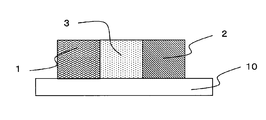
도 2는 본 발명의 콘덴서의 실시 형태의 하나를 나타낸 모식 단면도이다.
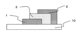
도 3은 본 발명의 콘덴서의 실시 형태의 하나를 나타낸 모식 단면도이다.
도 4는 본 발명의 콘덴서의 실시 형태의 하나를 나타낸 모식 단면도이다.
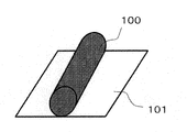
도 5a는 안테나 기판의 절곡 내성의 평가를 행할 때의 모식 사시도이다.
도 5b는 안테나 기판의 절곡 내성의 평가를 행할 때의 모식 사시도이다.


2: 도전막
3: 유전체층
10: 기판
100: 금속 원기둥
101: 안테나 기판
Claims (16)
- 적어도 한 쌍의 도전막과, 상기 한 쌍의 도전막간에 설치된 유전체층을 구비하는 콘덴서이며, 상기 유전체층이 유기 화합물과 금속 화합물을 함유하고, 상기 한 쌍의 도전막 중 적어도 한쪽의 도전막이 금속과 유기 화합물을 함유하는 것을 특징으로 하는 콘덴서.
- 제1항에 있어서, 상기 유전체층 중의 유기 화합물이 규소 원자와 탄소 원자의 결합을 갖는 콘덴서.
- 제1항 또는 제2항에 있어서, 상기 유전체층 중의 금속 화합물이 금속 원자와 산소 원자의 결합을 갖는 금속 화합물을 포함하는 콘덴서.
- 제3항에 있어서, 상기 유전체층이 탄소 원자와 규소 원자의 합계 100중량부에 대하여 금속 원자를 10 내지 180중량부 포함하는 콘덴서.
- 제3항 또는 제4항에 있어서, 상기 금속 원자가 알루미늄인 콘덴서.
- 제1항 내지 제5항 중 어느 한 항에 있어서, 상기 유전체층의 막 두께가 0.1㎛ 내지 5㎛인 콘덴서.
- 제1항 내지 제6항 중 어느 한 항에 있어서, 상기 도전막 중의 유기 화합물이 우레탄기를 갖는 콘덴서.
- 제1항 내지 제7항 중 어느 한 항에 기재된 콘덴서와, 트랜지스터를 적어도 갖는 회로.
- 제8항에 있어서, 트랜지스터가 게이트 절연층을 구비하고 있으며, 해당 게이트 절연층과 상기 유전체층이 동일 재료인 회로.
- 적어도 이하의 공정을 포함하는, 콘덴서의 제조 방법;
(1) 절연 기판 상에, 도전체와 감광성 유기 화합물을 함유하는 도전 페이스트를 사용하여 감광성 도전막을 형성하는 공정;
(2) 상기 감광성 도전막을, 포토리소그래피에 의해 콘덴서의 도전막에 대응하는 패턴으로 가공하는 공정;
(3) 유기 화합물과 금속 화합물을 함유하는 조성물을 도포 및 건조하여, 유전체층을 형성하는 공정. - 제10항에 있어서, 상기 조성물이 규소 원자와 탄소 원자의 결합을 갖는 화합물을 포함하는 콘덴서의 제조 방법.
- 제10항 또는 제11항에 있어서, 상기 조성물이, 중량 평균 분자량이 1000 이상인 중합체를 함유하는 조성물인 콘덴서의 제조 방법.
- 제10항 내지 제12항 중 어느 한 항에 있어서, 상기 조성물이 화학식 (1)로 표시되는 금속 킬레이트 화합물을 더 함유하는 조성물인 콘덴서의 제조 방법.
R1 xM(OR2)y-x (1)
(R1은 1가의 2좌 배위자를 나타내며, R1이 복수 존재하는 경우, 각각의 R1은 동일해도 상이해도 된다. R2는 수소 원자, 알킬기, 아실기 또는 아릴기를 나타내며, R2가 복수 존재하는 경우, 각각의 R2는 동일해도 상이해도 된다. M은 y가의 금속 원자를 나타낸다. y는 1 내지 6이다. x는 1 내지 y의 정수를 나타낸다.) - 제13항에 있어서, 상기 조성물이, 화학식 (1)로 표시되는 금속 킬레이트 화합물 100중량부에 대하여 중량 평균 분자량이 1000 이상인 중합체를 5 내지 90중량부 함유하는 조성물인 콘덴서의 제조 방법.
- 적어도 이하의 공정을 포함하는, 회로의 제조 방법;
(1) 절연 기판 상에, 콘덴서의 하부 전극과, 트랜지스터의 게이트 전극 또는 소스/드레인 전극을 형성하는 공정;
(2) 유기 화합물과 금속 화합물을 함유하는 조성물을 도포 및 건조하여, 콘덴서의 유전체층과 트랜지스터의 게이트 절연층을 동시에 형성하는 공정. - 제1항 내지 제7항 중 어느 한 항에 기재된 콘덴서, 및 트랜지스터 및 안테나 패턴을 적어도 갖는 무선 통신 장치.
Applications Claiming Priority (3)
| Application Number | Priority Date | Filing Date | Title |
|---|---|---|---|
| JP2015206916 | 2015-10-21 | ||
| JPJP-P-2015-206916 | 2015-10-21 | ||
| PCT/JP2016/080554 WO2017069059A1 (ja) | 2015-10-21 | 2016-10-14 | コンデンサおよびその製造方法ならびにそれを用いた無線通信装置 |
Publications (2)
| Publication Number | Publication Date |
|---|---|
| KR20180071283A true KR20180071283A (ko) | 2018-06-27 |
| KR102682010B1 KR102682010B1 (ko) | 2024-07-08 |
Family
ID=58557387
Family Applications (1)
| Application Number | Title | Priority Date | Filing Date |
|---|---|---|---|
| KR1020187012797A Active KR102682010B1 (ko) | 2015-10-21 | 2016-10-14 | 콘덴서 및 그의 제조 방법 및 그것을 사용한 무선 통신 장치 |
Country Status (7)
| Country | Link |
|---|---|
| US (1) | US10636866B2 (ko) |
| EP (1) | EP3367402B1 (ko) |
| JP (1) | JP6919198B2 (ko) |
| KR (1) | KR102682010B1 (ko) |
| CN (1) | CN108140484A (ko) |
| TW (1) | TWI743054B (ko) |
| WO (1) | WO2017069059A1 (ko) |
Cited By (1)
| Publication number | Priority date | Publication date | Assignee | Title |
|---|---|---|---|---|
| KR20200104481A (ko) * | 2019-02-26 | 2020-09-04 | 주식회사 디케이티 | 고분자 분산형 박막액정 표시장치 |
Families Citing this family (3)
| Publication number | Priority date | Publication date | Assignee | Title |
|---|---|---|---|---|
| US12542244B2 (en) | 2020-11-03 | 2026-02-03 | Zhi Neng Rong Dian (Beijing) Technology Co., Ltd | Flexible variable capacitor and method for preparation thereof |
| WO2025083999A1 (ja) * | 2023-10-18 | 2025-04-24 | パナソニックIpマネジメント株式会社 | 誘電体、キャパシタ、電気回路、回路基板、機器、及び蓄電デバイス |
| JP7656849B1 (ja) * | 2023-10-18 | 2025-04-04 | パナソニックIpマネジメント株式会社 | 誘電体、キャパシタ、電気回路、回路基板、機器、及び蓄電デバイス |
Citations (6)
| Publication number | Priority date | Publication date | Assignee | Title |
|---|---|---|---|---|
| JPH10112216A (ja) * | 1996-08-09 | 1998-04-28 | Toray Ind Inc | 感光性導電ペースト、それを用いた電極およびその製造方法 |
| JP2006309202A (ja) * | 2005-03-29 | 2006-11-09 | Toray Ind Inc | 感光性樹脂組成物およびそれを用いた半導体装置 |
| JP2008112147A (ja) * | 2006-09-27 | 2008-05-15 | Toray Ind Inc | 感光性樹脂組成物およびそれを用いた誘電体組成物、半導体装置 |
| JP2011519147A (ja) | 2007-10-10 | 2011-06-30 | コヴィオ インコーポレイテッド | 高信頼性監視及び/又は識別タグ/デバイス並びにかかるタグ/デバイスを作成する方法及び使用する方法 |
| JP2014160515A (ja) | 2007-10-10 | 2014-09-04 | Kovio Inc | プリント集積回路を含む無線デバイス並びにその製造及び使用方法 |
| WO2014142105A1 (ja) * | 2013-03-14 | 2014-09-18 | 東レ株式会社 | 電界効果型トランジスタ |
Family Cites Families (13)
| Publication number | Priority date | Publication date | Assignee | Title |
|---|---|---|---|---|
| JPH0520924A (ja) * | 1991-07-08 | 1993-01-29 | Olympus Optical Co Ltd | 有機誘電体ペーストおよびその製造方法 |
| KR100277382B1 (ko) * | 1995-08-18 | 2001-01-15 | 사토 히로시 | 다층전자부품 |
| JP4021021B2 (ja) * | 1997-10-21 | 2007-12-12 | 株式会社大紀アルミニウム工業所 | アルミニウム残灰からセラミック製品を製造する方法 |
| JP2000276945A (ja) * | 1999-03-25 | 2000-10-06 | Murata Mfg Co Ltd | 導体ペースト及びそれを用いた回路基板 |
| JP2005280287A (ja) * | 2004-03-31 | 2005-10-13 | Tokai Aluminum Foil Co Ltd | 共振ラベル用積層材の製造法 |
| US20070232734A1 (en) * | 2006-03-31 | 2007-10-04 | Karthikeyan Kanakarajan | Polyimide based compositions useful in high frequency circuitry applications and methods relating thereto |
| KR100829539B1 (ko) * | 2007-04-13 | 2008-05-16 | 삼성전자주식회사 | 박막 제조 방법, 이를 이용한 게이트 구조물 및 커패시터의제조 방법 |
| WO2009019979A1 (ja) * | 2007-08-09 | 2009-02-12 | Sekisui Chemical Co., Ltd. | 光硬化性組成物 |
| US20090230363A1 (en) * | 2007-11-14 | 2009-09-17 | Samsung Electro-Mechanics Co., Ltd. | Polymer composite |
| KR101420147B1 (ko) * | 2009-03-31 | 2014-07-21 | 주식회사 잉크테크 | 박막 캐패시터의 제조 방법 |
| CN104485336B (zh) * | 2009-10-21 | 2018-01-02 | 株式会社半导体能源研究所 | 半导体器件 |
| CN103193477B (zh) * | 2012-01-06 | 2016-03-16 | 三菱综合材料株式会社 | 介电薄膜形成用组合物、介电薄膜的形成方法及介电薄膜 |
| WO2016199886A1 (ja) * | 2015-06-11 | 2016-12-15 | 京セラ株式会社 | 複合樹脂材料、誘電体フィルムと、これを用いたフィルムコンデンサおよび連結型コンデンサ、ならびにインバータ、電動車輌 |
-
2016
- 2016-10-14 EP EP16857374.9A patent/EP3367402B1/en active Active
- 2016-10-14 US US15/764,197 patent/US10636866B2/en active Active
- 2016-10-14 JP JP2016563872A patent/JP6919198B2/ja active Active
- 2016-10-14 KR KR1020187012797A patent/KR102682010B1/ko active Active
- 2016-10-14 CN CN201680060860.1A patent/CN108140484A/zh active Pending
- 2016-10-14 WO PCT/JP2016/080554 patent/WO2017069059A1/ja not_active Ceased
- 2016-10-18 TW TW105133476A patent/TWI743054B/zh active
Patent Citations (6)
| Publication number | Priority date | Publication date | Assignee | Title |
|---|---|---|---|---|
| JPH10112216A (ja) * | 1996-08-09 | 1998-04-28 | Toray Ind Inc | 感光性導電ペースト、それを用いた電極およびその製造方法 |
| JP2006309202A (ja) * | 2005-03-29 | 2006-11-09 | Toray Ind Inc | 感光性樹脂組成物およびそれを用いた半導体装置 |
| JP2008112147A (ja) * | 2006-09-27 | 2008-05-15 | Toray Ind Inc | 感光性樹脂組成物およびそれを用いた誘電体組成物、半導体装置 |
| JP2011519147A (ja) | 2007-10-10 | 2011-06-30 | コヴィオ インコーポレイテッド | 高信頼性監視及び/又は識別タグ/デバイス並びにかかるタグ/デバイスを作成する方法及び使用する方法 |
| JP2014160515A (ja) | 2007-10-10 | 2014-09-04 | Kovio Inc | プリント集積回路を含む無線デバイス並びにその製造及び使用方法 |
| WO2014142105A1 (ja) * | 2013-03-14 | 2014-09-18 | 東レ株式会社 | 電界効果型トランジスタ |
Cited By (1)
| Publication number | Priority date | Publication date | Assignee | Title |
|---|---|---|---|---|
| KR20200104481A (ko) * | 2019-02-26 | 2020-09-04 | 주식회사 디케이티 | 고분자 분산형 박막액정 표시장치 |
Also Published As
| Publication number | Publication date |
|---|---|
| JP6919198B2 (ja) | 2021-08-18 |
| EP3367402A1 (en) | 2018-08-29 |
| EP3367402A4 (en) | 2019-03-13 |
| US10636866B2 (en) | 2020-04-28 |
| JPWO2017069059A1 (ja) | 2018-08-09 |
| KR102682010B1 (ko) | 2024-07-08 |
| US20180277619A1 (en) | 2018-09-27 |
| TW201721680A (zh) | 2017-06-16 |
| CN108140484A (zh) | 2018-06-08 |
| WO2017069059A1 (ja) | 2017-04-27 |
| TWI743054B (zh) | 2021-10-21 |
| EP3367402B1 (en) | 2021-07-07 |
Similar Documents
| Publication | Publication Date | Title |
|---|---|---|
| CN109716491B (zh) | 场效应晶体管的制造方法及无线通信设备的制造方法 | |
| JP6766649B2 (ja) | アンテナ基板の製造方法、配線と電極付きアンテナ基板の製造方法およびrfid素子の製造方法 | |
| US10490748B2 (en) | Rectifying element, method for producing same, and wireless communication device | |
| KR102566164B1 (ko) | 전계 효과형 트랜지스터, 그의 제조 방법, 그것을 사용한 무선 통신 장치 및 상품 태그 | |
| KR20180088414A (ko) | 강유전체 기억 소자, 그의 제조 방법, 및 그것을 사용한 메모리 셀 및 그것을 사용한 무선 통신 장치 | |
| TWI570186B (zh) | A composition for an organic semiconductor insulating film, and an organic semiconductor insulating film | |
| JP6332573B1 (ja) | 電界効果型トランジスタ、その製造方法、それを用いた無線通信装置および商品タグ | |
| JP6919198B2 (ja) | コンデンサおよびその製造方法ならびにそれを用いた無線通信装置 | |
| JP2021055049A (ja) | 樹脂組成物、それを用いた素子の製造方法 | |
| JP7739814B2 (ja) | 素子およびその製造方法、無線通信装置および薄膜トランジスタアレイ |
Legal Events
| Date | Code | Title | Description |
|---|---|---|---|
| PA0105 | International application |
Patent event date: 20180504 Patent event code: PA01051R01D Comment text: International Patent Application |
|
| PG1501 | Laying open of application | ||
| A201 | Request for examination | ||
| PA0201 | Request for examination |
Patent event code: PA02012R01D Patent event date: 20211007 Comment text: Request for Examination of Application |
|
| E902 | Notification of reason for refusal | ||
| PE0902 | Notice of grounds for rejection |
Comment text: Notification of reason for refusal Patent event date: 20231113 Patent event code: PE09021S01D |
|
| E701 | Decision to grant or registration of patent right | ||
| PE0701 | Decision of registration |
Patent event code: PE07011S01D Comment text: Decision to Grant Registration Patent event date: 20240613 |
|
| GRNT | Written decision to grant | ||
| PR0701 | Registration of establishment |
Comment text: Registration of Establishment Patent event date: 20240702 Patent event code: PR07011E01D |
|
| PR1002 | Payment of registration fee |
Payment date: 20240703 End annual number: 3 Start annual number: 1 |
|
| PG1601 | Publication of registration |