KR20190000007A - 리지드 플렉시블 회로기판 제조방법 - Google Patents
리지드 플렉시블 회로기판 제조방법 Download PDFInfo
- Publication number
- KR20190000007A KR20190000007A KR1020170078483A KR20170078483A KR20190000007A KR 20190000007 A KR20190000007 A KR 20190000007A KR 1020170078483 A KR1020170078483 A KR 1020170078483A KR 20170078483 A KR20170078483 A KR 20170078483A KR 20190000007 A KR20190000007 A KR 20190000007A
- Authority
- KR
- South Korea
- Prior art keywords
- circuit board
- flexible
- circuit
- release film
- boundary
- Prior art date
- Legal status (The legal status is an assumption and is not a legal conclusion. Google has not performed a legal analysis and makes no representation as to the accuracy of the status listed.)
- Granted
Links
Images

Classifications
-
- H—ELECTRICITY
- H05—ELECTRIC TECHNIQUES NOT OTHERWISE PROVIDED FOR
- H05K—PRINTED CIRCUITS; CASINGS OR CONSTRUCTIONAL DETAILS OF ELECTRIC APPARATUS; MANUFACTURE OF ASSEMBLAGES OF ELECTRICAL COMPONENTS
- H05K3/00—Apparatus or processes for manufacturing printed circuits
- H05K3/46—Manufacturing multilayer circuits
- H05K3/4688—Composite multilayer circuits, i.e. comprising insulating layers having different properties
- H05K3/4691—Rigid-flexible multilayer circuits comprising rigid and flexible layers, e.g. having in the bending regions only flexible layers
-
- H—ELECTRICITY
- H05—ELECTRIC TECHNIQUES NOT OTHERWISE PROVIDED FOR
- H05K—PRINTED CIRCUITS; CASINGS OR CONSTRUCTIONAL DETAILS OF ELECTRIC APPARATUS; MANUFACTURE OF ASSEMBLAGES OF ELECTRICAL COMPONENTS
- H05K3/00—Apparatus or processes for manufacturing printed circuits
- H05K3/0011—Working of insulating substrates or insulating layers
- H05K3/0044—Mechanical working of the substrate, e.g. drilling or punching
-
- H—ELECTRICITY
- H05—ELECTRIC TECHNIQUES NOT OTHERWISE PROVIDED FOR
- H05K—PRINTED CIRCUITS; CASINGS OR CONSTRUCTIONAL DETAILS OF ELECTRIC APPARATUS; MANUFACTURE OF ASSEMBLAGES OF ELECTRICAL COMPONENTS
- H05K3/00—Apparatus or processes for manufacturing printed circuits
- H05K3/46—Manufacturing multilayer circuits
- H05K3/4697—Manufacturing multilayer circuits having cavities, e.g. for mounting components
Landscapes
- Engineering & Computer Science (AREA)
- Manufacturing & Machinery (AREA)
- Microelectronics & Electronic Packaging (AREA)
- Production Of Multi-Layered Print Wiring Board (AREA)
Abstract
Description
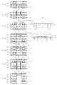
도 2는 본 발명의 일 실시예에 따라 리지드 플렉시블 회로기판 제조되는 과정을 간략하게 보인 예시도이다.
11: 코어
12: 제1절연층
13: 제1내층회로
14: 경계홀
20: 이형필름
30: 외층회로층
31: 제2절연층
32: 보강대
Claims (5)
- a)제1내층회로를 형성한 회로기판을 준비하는 단계;
b)상기 회로기판 상부에서 플렉시블 영역의 경계에 라우터 공정으로 경계홀을 형성하는 단계;
c)상기 회로기판 중 경계홀이 형성된 플렉시블 영역에 이형필름을 가접하는 단계;
d)상기 회로기판의 상, 하측에 각각 복수 개의 외층회로층을 형성하는 단계;
e)상기 회로기판의 하부에서 플렉시블 영역의 경계에 뎁스라우터 공정을 실시하는 단계; 및
f)상기 뎁스라우터 공정에 의해 형성된 플렉시블 영역의 캡과 이형필름을 제거하여 플렉시블 영역의 캐비티를 형성하는 단계;를 포함하는 리지드 플렉시블 회로기판 제조방법.
- 청구항 1에 있어서,
상기 a)단계에서 상기 회로기판은
코어를 기준으로 상기 코어의 상, 하면에 각각 적층된 제1절연층과;
상기 코어의 상, 하면에 각각 적층된 제1절연층의 상, 하측에 각각 형성된 제1내층회로를 포함하는 리지드 플렉시블 회로기판 제조방법.
- 청구항 2에 있어서,
상기 b)단계에서 상기 경계홀은
상기 회로기판의 상부에서 시작하여 제1내층회로 및 제1절연층을 관통하여 형성되는 것을 특징으로 하는 리지드 플렉시블 회로기판 제조방법.
- 청구항 1에 있어서,
상기 c)단계에서 상기 이형필름의 주변은
상기 플렉시블 영역의 경계홀 상에 위치하여, 절연층 또는 회로층의 적층이 이루어질 시, 상기 경계홀로 굴곡되는 것을 특징으로 하는 리지드 플렉시블 회로기판 제조방법.
- 청구항1에 있어서,
상기 e)단계에서 상기 뎁스라우터 공정의 가공 깊이는
상기 경계홀의 하단까지 실시하는 것을 특징으로 하는 리지드 플렉시블 회로기판 제조방법.
Priority Applications (1)
| Application Number | Priority Date | Filing Date | Title |
|---|---|---|---|
| KR1020170078483A KR101969643B1 (ko) | 2017-06-21 | 2017-06-21 | 리지드 플렉시블 회로기판 제조방법 |
Applications Claiming Priority (1)
| Application Number | Priority Date | Filing Date | Title |
|---|---|---|---|
| KR1020170078483A KR101969643B1 (ko) | 2017-06-21 | 2017-06-21 | 리지드 플렉시블 회로기판 제조방법 |
Publications (2)
| Publication Number | Publication Date |
|---|---|
| KR20190000007A true KR20190000007A (ko) | 2019-01-02 |
| KR101969643B1 KR101969643B1 (ko) | 2019-04-17 |
Family
ID=65021581
Family Applications (1)
| Application Number | Title | Priority Date | Filing Date |
|---|---|---|---|
| KR1020170078483A Expired - Fee Related KR101969643B1 (ko) | 2017-06-21 | 2017-06-21 | 리지드 플렉시블 회로기판 제조방법 |
Country Status (1)
| Country | Link |
|---|---|
| KR (1) | KR101969643B1 (ko) |
Cited By (1)
| Publication number | Priority date | Publication date | Assignee | Title |
|---|---|---|---|---|
| CN118076012A (zh) * | 2024-03-11 | 2024-05-24 | 九江明阳电路科技有限公司 | 一种不对称结构刚挠板翘曲程度的控制方法 |
Citations (2)
| Publication number | Priority date | Publication date | Assignee | Title |
|---|---|---|---|---|
| JP3820415B2 (ja) * | 2002-03-07 | 2006-09-13 | 株式会社デンソー | プリント基板の製造方法及びプリント基板の構造 |
| JP2015061003A (ja) * | 2013-09-20 | 2015-03-30 | 日本シイエムケイ株式会社 | リジッドフレックス多層プリント配線板の製造方法 |
-
2017
- 2017-06-21 KR KR1020170078483A patent/KR101969643B1/ko not_active Expired - Fee Related
Patent Citations (2)
| Publication number | Priority date | Publication date | Assignee | Title |
|---|---|---|---|---|
| JP3820415B2 (ja) * | 2002-03-07 | 2006-09-13 | 株式会社デンソー | プリント基板の製造方法及びプリント基板の構造 |
| JP2015061003A (ja) * | 2013-09-20 | 2015-03-30 | 日本シイエムケイ株式会社 | リジッドフレックス多層プリント配線板の製造方法 |
Cited By (1)
| Publication number | Priority date | Publication date | Assignee | Title |
|---|---|---|---|---|
| CN118076012A (zh) * | 2024-03-11 | 2024-05-24 | 九江明阳电路科技有限公司 | 一种不对称结构刚挠板翘曲程度的控制方法 |
Also Published As
| Publication number | Publication date |
|---|---|
| KR101969643B1 (ko) | 2019-04-17 |
Similar Documents
| Publication | Publication Date | Title |
|---|---|---|
| JP4150396B2 (ja) | リジッドフレキシブル基板の製造方法 | |
| US10034368B2 (en) | Flying tail type rigid-flexible printed circuit board | |
| JP6373574B2 (ja) | 回路基板及びその製造方法 | |
| US8099865B2 (en) | Method for manufacturing a circuit board having an embedded component therein | |
| US20100142170A1 (en) | Chip embedded printed circuit board and manufacturing method thereof | |
| JP5088138B2 (ja) | 実装基板および電子機器 | |
| US20140353014A1 (en) | Combined circuit board and method of manufacturing the same | |
| CN101170878A (zh) | 制造印刷电路板的方法 | |
| JP2009277916A (ja) | 配線基板及びその製造方法並びに半導体パッケージ | |
| JP2012134490A (ja) | 電子部品内蔵型リジッドフレキシブルプリント回路基板の製造方法 | |
| TWI513379B (zh) | 內埋元件的基板結構與其製造方法 | |
| KR100820633B1 (ko) | 전자소자 내장 인쇄회로기판 및 그 제조방법 | |
| JP6607087B2 (ja) | 電子部品内蔵基板の製造方法 | |
| KR20090096809A (ko) | 반도체 부품 내장형 인쇄회로기판 제조 방법 | |
| CN101499453B (zh) | 配线电路基板及其制造方法 | |
| JP4934444B2 (ja) | 半導体装置とその製造方法 | |
| KR101969643B1 (ko) | 리지드 플렉시블 회로기판 제조방법 | |
| KR20090102119A (ko) | 임베디드 인쇄회로기판 및 그 제조방법 | |
| KR20130055990A (ko) | 리지드-플렉서블 인쇄회로기판 및 그 제조방법 | |
| KR101077430B1 (ko) | 리지드-플렉시블 기판의 제조방법 | |
| CN114258200B (zh) | 具有内埋元件的软硬结合线路板的制作方法 | |
| KR20060042723A (ko) | 경연성 다층 인쇄회로기판의 제조 방법 | |
| KR102023729B1 (ko) | 인쇄회로기판 및 그 제조 방법 | |
| KR101038335B1 (ko) | 다층 인쇄회로기판의 제조방법 | |
| KR100704911B1 (ko) | 전자소자 내장형 인쇄회로기판 및 그 제조방법 |
Legal Events
| Date | Code | Title | Description |
|---|---|---|---|
| A201 | Request for examination | ||
| PA0109 | Patent application |
St.27 status event code: A-0-1-A10-A12-nap-PA0109 |
|
| PA0201 | Request for examination |
St.27 status event code: A-1-2-D10-D11-exm-PA0201 |
|
| PN2301 | Change of applicant |
St.27 status event code: A-3-3-R10-R13-asn-PN2301 St.27 status event code: A-3-3-R10-R11-asn-PN2301 |
|
| D13-X000 | Search requested |
St.27 status event code: A-1-2-D10-D13-srh-X000 |
|
| D14-X000 | Search report completed |
St.27 status event code: A-1-2-D10-D14-srh-X000 |
|
| E902 | Notification of reason for refusal | ||
| PE0902 | Notice of grounds for rejection |
St.27 status event code: A-1-2-D10-D21-exm-PE0902 |
|
| E13-X000 | Pre-grant limitation requested |
St.27 status event code: A-2-3-E10-E13-lim-X000 |
|
| P11-X000 | Amendment of application requested |
St.27 status event code: A-2-2-P10-P11-nap-X000 |
|
| P13-X000 | Application amended |
St.27 status event code: A-2-2-P10-P13-nap-X000 |
|
| PG1501 | Laying open of application |
St.27 status event code: A-1-1-Q10-Q12-nap-PG1501 |
|
| E701 | Decision to grant or registration of patent right | ||
| PE0701 | Decision of registration |
St.27 status event code: A-1-2-D10-D22-exm-PE0701 |
|
| GRNT | Written decision to grant | ||
| PR0701 | Registration of establishment |
St.27 status event code: A-2-4-F10-F11-exm-PR0701 |
|
| PR1002 | Payment of registration fee |
St.27 status event code: A-2-2-U10-U11-oth-PR1002 Fee payment year number: 1 |
|
| PG1601 | Publication of registration |
St.27 status event code: A-4-4-Q10-Q13-nap-PG1601 |
|
| PC1903 | Unpaid annual fee |
St.27 status event code: A-4-4-U10-U13-oth-PC1903 Not in force date: 20220411 Payment event data comment text: Termination Category : DEFAULT_OF_REGISTRATION_FEE |
|
| PC1903 | Unpaid annual fee |
St.27 status event code: N-4-6-H10-H13-oth-PC1903 Ip right cessation event data comment text: Termination Category : DEFAULT_OF_REGISTRATION_FEE Not in force date: 20220411 |