KR20190004231A - 저주파 rf 전력의 분포 조절 기능을 갖는 플라즈마 반응기 및 이에 적용되는 방법 - Google Patents
저주파 rf 전력의 분포 조절 기능을 갖는 플라즈마 반응기 및 이에 적용되는 방법 Download PDFInfo
- Publication number
- KR20190004231A KR20190004231A KR1020180076328A KR20180076328A KR20190004231A KR 20190004231 A KR20190004231 A KR 20190004231A KR 1020180076328 A KR1020180076328 A KR 1020180076328A KR 20180076328 A KR20180076328 A KR 20180076328A KR 20190004231 A KR20190004231 A KR 20190004231A
- Authority
- KR
- South Korea
- Prior art keywords
- conductive
- ring
- plasma
- focusing ring
- low frequency
- Prior art date
- Legal status (The legal status is an assumption and is not a legal conclusion. Google has not performed a legal analysis and makes no representation as to the accuracy of the status listed.)
- Granted
Links
Images



Classifications
-
- H—ELECTRICITY
- H01—ELECTRIC ELEMENTS
- H01J—ELECTRIC DISCHARGE TUBES OR DISCHARGE LAMPS
- H01J37/00—Discharge tubes with provision for introducing objects or material to be exposed to the discharge, e.g. for the purpose of examination or processing thereof
- H01J37/32—Gas-filled discharge tubes
- H01J37/32009—Arrangements for generation of plasma specially adapted for examination or treatment of objects, e.g. plasma sources
- H01J37/32082—Radio frequency generated discharge
- H01J37/32137—Radio frequency generated discharge controlling of the discharge by modulation of energy
-
- H—ELECTRICITY
- H01—ELECTRIC ELEMENTS
- H01J—ELECTRIC DISCHARGE TUBES OR DISCHARGE LAMPS
- H01J37/00—Discharge tubes with provision for introducing objects or material to be exposed to the discharge, e.g. for the purpose of examination or processing thereof
- H01J37/32—Gas-filled discharge tubes
- H01J37/32431—Constructional details of the reactor
- H01J37/32623—Mechanical discharge control means
- H01J37/32642—Focus rings
-
- C—CHEMISTRY; METALLURGY
- C23—COATING METALLIC MATERIAL; COATING MATERIAL WITH METALLIC MATERIAL; CHEMICAL SURFACE TREATMENT; DIFFUSION TREATMENT OF METALLIC MATERIAL; COATING BY VACUUM EVAPORATION, BY SPUTTERING, BY ION IMPLANTATION OR BY CHEMICAL VAPOUR DEPOSITION, IN GENERAL; INHIBITING CORROSION OF METALLIC MATERIAL OR INCRUSTATION IN GENERAL
- C23C—COATING METALLIC MATERIAL; COATING MATERIAL WITH METALLIC MATERIAL; SURFACE TREATMENT OF METALLIC MATERIAL BY DIFFUSION INTO THE SURFACE, BY CHEMICAL CONVERSION OR SUBSTITUTION; COATING BY VACUUM EVAPORATION, BY SPUTTERING, BY ION IMPLANTATION OR BY CHEMICAL VAPOUR DEPOSITION, IN GENERAL
- C23C16/00—Chemical coating by decomposition of gaseous compounds, without leaving reaction products of surface material in the coating, i.e. chemical vapour deposition [CVD] processes
- C23C16/44—Chemical coating by decomposition of gaseous compounds, without leaving reaction products of surface material in the coating, i.e. chemical vapour deposition [CVD] processes characterised by the method of coating
- C23C16/50—Chemical coating by decomposition of gaseous compounds, without leaving reaction products of surface material in the coating, i.e. chemical vapour deposition [CVD] processes characterised by the method of coating using electric discharges
- C23C16/505—Chemical coating by decomposition of gaseous compounds, without leaving reaction products of surface material in the coating, i.e. chemical vapour deposition [CVD] processes characterised by the method of coating using electric discharges using radio frequency discharges
-
- C—CHEMISTRY; METALLURGY
- C23—COATING METALLIC MATERIAL; COATING MATERIAL WITH METALLIC MATERIAL; CHEMICAL SURFACE TREATMENT; DIFFUSION TREATMENT OF METALLIC MATERIAL; COATING BY VACUUM EVAPORATION, BY SPUTTERING, BY ION IMPLANTATION OR BY CHEMICAL VAPOUR DEPOSITION, IN GENERAL; INHIBITING CORROSION OF METALLIC MATERIAL OR INCRUSTATION IN GENERAL
- C23C—COATING METALLIC MATERIAL; COATING MATERIAL WITH METALLIC MATERIAL; SURFACE TREATMENT OF METALLIC MATERIAL BY DIFFUSION INTO THE SURFACE, BY CHEMICAL CONVERSION OR SUBSTITUTION; COATING BY VACUUM EVAPORATION, BY SPUTTERING, BY ION IMPLANTATION OR BY CHEMICAL VAPOUR DEPOSITION, IN GENERAL
- C23C16/00—Chemical coating by decomposition of gaseous compounds, without leaving reaction products of surface material in the coating, i.e. chemical vapour deposition [CVD] processes
- C23C16/44—Chemical coating by decomposition of gaseous compounds, without leaving reaction products of surface material in the coating, i.e. chemical vapour deposition [CVD] processes characterised by the method of coating
- C23C16/50—Chemical coating by decomposition of gaseous compounds, without leaving reaction products of surface material in the coating, i.e. chemical vapour deposition [CVD] processes characterised by the method of coating using electric discharges
- C23C16/505—Chemical coating by decomposition of gaseous compounds, without leaving reaction products of surface material in the coating, i.e. chemical vapour deposition [CVD] processes characterised by the method of coating using electric discharges using radio frequency discharges
- C23C16/509—Chemical coating by decomposition of gaseous compounds, without leaving reaction products of surface material in the coating, i.e. chemical vapour deposition [CVD] processes characterised by the method of coating using electric discharges using radio frequency discharges using internal electrodes
-
- H—ELECTRICITY
- H01—ELECTRIC ELEMENTS
- H01J—ELECTRIC DISCHARGE TUBES OR DISCHARGE LAMPS
- H01J37/00—Discharge tubes with provision for introducing objects or material to be exposed to the discharge, e.g. for the purpose of examination or processing thereof
- H01J37/32—Gas-filled discharge tubes
- H01J37/32009—Arrangements for generation of plasma specially adapted for examination or treatment of objects, e.g. plasma sources
- H01J37/32082—Radio frequency generated discharge
-
- H—ELECTRICITY
- H01—ELECTRIC ELEMENTS
- H01J—ELECTRIC DISCHARGE TUBES OR DISCHARGE LAMPS
- H01J37/00—Discharge tubes with provision for introducing objects or material to be exposed to the discharge, e.g. for the purpose of examination or processing thereof
- H01J37/32—Gas-filled discharge tubes
- H01J37/32009—Arrangements for generation of plasma specially adapted for examination or treatment of objects, e.g. plasma sources
- H01J37/32082—Radio frequency generated discharge
- H01J37/32137—Radio frequency generated discharge controlling of the discharge by modulation of energy
- H01J37/32155—Frequency modulation
-
- H—ELECTRICITY
- H01—ELECTRIC ELEMENTS
- H01J—ELECTRIC DISCHARGE TUBES OR DISCHARGE LAMPS
- H01J37/00—Discharge tubes with provision for introducing objects or material to be exposed to the discharge, e.g. for the purpose of examination or processing thereof
- H01J37/32—Gas-filled discharge tubes
- H01J37/32009—Arrangements for generation of plasma specially adapted for examination or treatment of objects, e.g. plasma sources
- H01J37/32082—Radio frequency generated discharge
- H01J37/32174—Circuits specially adapted for controlling the RF discharge
- H01J37/32183—Matching circuits
-
- H—ELECTRICITY
- H01—ELECTRIC ELEMENTS
- H01J—ELECTRIC DISCHARGE TUBES OR DISCHARGE LAMPS
- H01J37/00—Discharge tubes with provision for introducing objects or material to be exposed to the discharge, e.g. for the purpose of examination or processing thereof
- H01J37/32—Gas-filled discharge tubes
- H01J37/32009—Arrangements for generation of plasma specially adapted for examination or treatment of objects, e.g. plasma sources
- H01J37/32366—Localised processing
- H01J37/32385—Treating the edge of the workpieces
-
- H—ELECTRICITY
- H01—ELECTRIC ELEMENTS
- H01J—ELECTRIC DISCHARGE TUBES OR DISCHARGE LAMPS
- H01J37/00—Discharge tubes with provision for introducing objects or material to be exposed to the discharge, e.g. for the purpose of examination or processing thereof
- H01J37/32—Gas-filled discharge tubes
- H01J37/32431—Constructional details of the reactor
- H01J37/32458—Vessel
- H01J37/32477—Vessel characterised by the means for protecting vessels or internal parts, e.g. coatings
- H01J37/32495—Means for protecting the vessel against plasma
-
- H—ELECTRICITY
- H01—ELECTRIC ELEMENTS
- H01J—ELECTRIC DISCHARGE TUBES OR DISCHARGE LAMPS
- H01J37/00—Discharge tubes with provision for introducing objects or material to be exposed to the discharge, e.g. for the purpose of examination or processing thereof
- H01J37/32—Gas-filled discharge tubes
- H01J37/32431—Constructional details of the reactor
- H01J37/32532—Electrodes
- H01J37/32541—Shape
-
- H—ELECTRICITY
- H01—ELECTRIC ELEMENTS
- H01J—ELECTRIC DISCHARGE TUBES OR DISCHARGE LAMPS
- H01J37/00—Discharge tubes with provision for introducing objects or material to be exposed to the discharge, e.g. for the purpose of examination or processing thereof
- H01J37/32—Gas-filled discharge tubes
- H01J37/32431—Constructional details of the reactor
- H01J37/32532—Electrodes
- H01J37/32577—Electrical connecting means
-
- H—ELECTRICITY
- H01—ELECTRIC ELEMENTS
- H01J—ELECTRIC DISCHARGE TUBES OR DISCHARGE LAMPS
- H01J37/00—Discharge tubes with provision for introducing objects or material to be exposed to the discharge, e.g. for the purpose of examination or processing thereof
- H01J37/32—Gas-filled discharge tubes
- H01J37/32917—Plasma diagnostics
- H01J37/32935—Monitoring and controlling tubes by information coming from the object and/or discharge
- H01J37/32963—End-point detection
-
- H—ELECTRICITY
- H10—SEMICONDUCTOR DEVICES; ELECTRIC SOLID-STATE DEVICES NOT OTHERWISE PROVIDED FOR
- H10P—GENERIC PROCESSES OR APPARATUS FOR THE MANUFACTURE OR TREATMENT OF DEVICES COVERED BY CLASS H10
- H10P72/00—Handling or holding of wafers, substrates or devices during manufacture or treatment thereof
- H10P72/70—Handling or holding of wafers, substrates or devices during manufacture or treatment thereof for supporting or gripping
- H10P72/72—Handling or holding of wafers, substrates or devices during manufacture or treatment thereof for supporting or gripping using electrostatic chucks
-
- H—ELECTRICITY
- H10—SEMICONDUCTOR DEVICES; ELECTRIC SOLID-STATE DEVICES NOT OTHERWISE PROVIDED FOR
- H10P—GENERIC PROCESSES OR APPARATUS FOR THE MANUFACTURE OR TREATMENT OF DEVICES COVERED BY CLASS H10
- H10P72/00—Handling or holding of wafers, substrates or devices during manufacture or treatment thereof
- H10P72/70—Handling or holding of wafers, substrates or devices during manufacture or treatment thereof for supporting or gripping
- H10P72/72—Handling or holding of wafers, substrates or devices during manufacture or treatment thereof for supporting or gripping using electrostatic chucks
- H10P72/722—Details of electrostatic chucks
-
- H—ELECTRICITY
- H10—SEMICONDUCTOR DEVICES; ELECTRIC SOLID-STATE DEVICES NOT OTHERWISE PROVIDED FOR
- H10P—GENERIC PROCESSES OR APPARATUS FOR THE MANUFACTURE OR TREATMENT OF DEVICES COVERED BY CLASS H10
- H10P72/00—Handling or holding of wafers, substrates or devices during manufacture or treatment thereof
- H10P72/70—Handling or holding of wafers, substrates or devices during manufacture or treatment thereof for supporting or gripping
- H10P72/76—Handling or holding of wafers, substrates or devices during manufacture or treatment thereof for supporting or gripping using mechanical means, e.g. clamps or pinches
- H10P72/7604—Handling or holding of wafers, substrates or devices during manufacture or treatment thereof for supporting or gripping using mechanical means, e.g. clamps or pinches the wafers being placed on a susceptor, stage or support
- H10P72/7606—Handling or holding of wafers, substrates or devices during manufacture or treatment thereof for supporting or gripping using mechanical means, e.g. clamps or pinches the wafers being placed on a susceptor, stage or support characterised by edge clamping, e.g. clamping ring
-
- B—PERFORMING OPERATIONS; TRANSPORTING
- B05—SPRAYING OR ATOMISING IN GENERAL; APPLYING FLUENT MATERIALS TO SURFACES, IN GENERAL
- B05C—APPARATUS FOR APPLYING FLUENT MATERIALS TO SURFACES, IN GENERAL
- B05C13/00—Means for manipulating or holding work, e.g. for separate articles
- B05C13/02—Means for manipulating or holding work, e.g. for separate articles for particular articles
-
- H—ELECTRICITY
- H01—ELECTRIC ELEMENTS
- H01J—ELECTRIC DISCHARGE TUBES OR DISCHARGE LAMPS
- H01J2237/00—Discharge tubes exposing object to beam, e.g. for analysis treatment, etching, imaging
- H01J2237/20—Positioning, supporting, modifying or maintaining the physical state of objects being observed or treated
- H01J2237/2007—Holding mechanisms
-
- H—ELECTRICITY
- H01—ELECTRIC ELEMENTS
- H01J—ELECTRIC DISCHARGE TUBES OR DISCHARGE LAMPS
- H01J2237/00—Discharge tubes exposing object to beam, e.g. for analysis treatment, etching, imaging
- H01J2237/32—Processing objects by plasma generation
- H01J2237/33—Processing objects by plasma generation characterised by the type of processing
- H01J2237/334—Etching
- H01J2237/3341—Reactive etching
-
- H—ELECTRICITY
- H01—ELECTRIC ELEMENTS
- H01J—ELECTRIC DISCHARGE TUBES OR DISCHARGE LAMPS
- H01J37/00—Discharge tubes with provision for introducing objects or material to be exposed to the discharge, e.g. for the purpose of examination or processing thereof
- H01J37/32—Gas-filled discharge tubes
- H01J37/32009—Arrangements for generation of plasma specially adapted for examination or treatment of objects, e.g. plasma sources
- H01J37/32082—Radio frequency generated discharge
- H01J37/32091—Radio frequency generated discharge the radio frequency energy being capacitively coupled to the plasma
-
- H—ELECTRICITY
- H01—ELECTRIC ELEMENTS
- H01J—ELECTRIC DISCHARGE TUBES OR DISCHARGE LAMPS
- H01J37/00—Discharge tubes with provision for introducing objects or material to be exposed to the discharge, e.g. for the purpose of examination or processing thereof
- H01J37/32—Gas-filled discharge tubes
- H01J37/32009—Arrangements for generation of plasma specially adapted for examination or treatment of objects, e.g. plasma sources
- H01J37/32082—Radio frequency generated discharge
- H01J37/32137—Radio frequency generated discharge controlling of the discharge by modulation of energy
- H01J37/32155—Frequency modulation
- H01J37/32165—Plural frequencies
-
- H—ELECTRICITY
- H01—ELECTRIC ELEMENTS
- H01J—ELECTRIC DISCHARGE TUBES OR DISCHARGE LAMPS
- H01J37/00—Discharge tubes with provision for introducing objects or material to be exposed to the discharge, e.g. for the purpose of examination or processing thereof
- H01J37/32—Gas-filled discharge tubes
- H01J37/32009—Arrangements for generation of plasma specially adapted for examination or treatment of objects, e.g. plasma sources
- H01J37/32082—Radio frequency generated discharge
- H01J37/32174—Circuits specially adapted for controlling the RF discharge
-
- H—ELECTRICITY
- H01—ELECTRIC ELEMENTS
- H01J—ELECTRIC DISCHARGE TUBES OR DISCHARGE LAMPS
- H01J37/00—Discharge tubes with provision for introducing objects or material to be exposed to the discharge, e.g. for the purpose of examination or processing thereof
- H01J37/32—Gas-filled discharge tubes
- H01J37/32431—Constructional details of the reactor
- H01J37/32715—Workpiece holder
Landscapes
- Chemical & Material Sciences (AREA)
- Engineering & Computer Science (AREA)
- Physics & Mathematics (AREA)
- Plasma & Fusion (AREA)
- Analytical Chemistry (AREA)
- Chemical Kinetics & Catalysis (AREA)
- General Chemical & Material Sciences (AREA)
- Materials Engineering (AREA)
- Mechanical Engineering (AREA)
- Metallurgy (AREA)
- Organic Chemistry (AREA)
- Plasma Technology (AREA)
- Drying Of Semiconductors (AREA)
Abstract
Description
도1b는 종래 기술인 플라즈마 프로세싱 장치의 저주파로 생성한 RF 전력의 분포를 나타낸다.
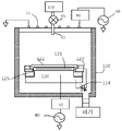
도2a는 본 발명에 의한 플라즈마 프로세싱 장치 구조를 나타낸다.
도2b는 본 발명에 의한 플라즈마 프로세싱 장치의 저주파로 생성한 RF 전력의 분포를 나타낸다.
도3은 본 발명에 의한 플라즈마 프로세싱 장치의 다른 일 실시예를 나타낸다.
도4는 본 발명에 의한 플라즈마 프로세싱 장치의 제3 실시예를 나타낸다.
도5는 본 발명에 의한 플라즈마 프로세싱 장치의 제4 실시예를 나타낸다.
Claims (20)
- 저주파 RF 전력의 분포 조절 기능을 갖는 플라즈마 반응기로서,
내부에 도전 베이스를 갖추고 상기 도전 베이스는 제1 정합기를 통하여 저주파의 RF공급원과 연결하고, 상기 도전 베이스 상에 ESC (electrostatic chuck) 을 포함하고 ESC의 상부 표면에 가공될 기판을 고정하고, 커플링 링이 상기 도전 베이스의 주위를 둘러싸고 포커싱 링이 상기 커플링 링의 상방향에 설치되며, 상기 포커싱 링이 상기 ESC을 둘러싸고 플라즈마 프로세싱 과정중에 플라즈마에 노출되는 반응 챔버;
상기 커플링 링의 위에 위치한 고리형 전극; 및
도전 연결부를 포함하되,
상기 도전 연결부는 적어도 도선을 포함하고, 제1 단자는 상기 도전 베이스와 연결되거나 상기 도전 베이스와 전기 결합된 도전부와 연결되고, 제 2 단자는 고리형 전극과 연결되고 가변 임피던스가 상기 도선에 직렬연결된 플라즈마 반응기.
- 제1항에 있어서,
상기 도전 베이스의 주변 하부에 단차부가 포함되고 상기 도전부는 상기 단차부의 상부에 위치하며 상기 커플링 링은 절연재질로 제조되어 상기 도전부의 상부에 설치하고, 상기 도전 베이스의 외측벽에는 적어도 한층의 플라즈마 부식에 견디는 절연재료층을 포함하는 것을 특징으로 하는 플라즈마 반응기.
- 제1항에 있어서,
상기 고리형 전극은 상기 포커싱 링의 하부에 위치하는 것을 특징으로 하는 플라즈마 반응기.
- 제1항에 있어서,
상기 포커싱 링은 절연재질로 제조되고 상기 고리형 전극이 상기 포커싱 링의 내부에 설치되는 것을 특징으로 하는 플라즈마 반응기.
- 제1항에 있어서,
상기 고리형 전극이 상기 커플링 링의 내부의 상반부에 설치하는 것을 특징으로 하는 플라즈마 반응기.
- 저주파 RF 전력의 분포 조절 기능을 갖는 플라즈마 반응기로서,
내부에 도전 베이스를 갖추고 상기 도전 베이스는 제1 정합기를 통하여 저주파의 RF공급원과 연결하고, 상기 도전 베이스 위에는 ESC을 포함하고 상기 ESC의 상부 표면에 가공될 기판을 고정하고, 커플링 링이 도전 베이스의 주위를 둘러싸고 포커싱 링이 상기 커플링 링의 위에 설치되어 상기 포커싱 링이 상기 ESC을 둘러싸고 플라즈마 프로세싱 과정중에 플라즈마에 노출되며, 상기 포커싱 링은 도체 또는 반도체 재질로 만들어지는 반응 챔버; 및
적어도 하나의 도선을 포함하되,
상기 도선의 제1 단자는 상기 도전 베이스와 연결되거나 상기 도전 베이스와 전기 결합된 도전부와 연결되고, 상기 도선의 제 2 단자는 상기 포커싱 링과 연결되며, 가변 임피던스가 상기 도선에 직렬연결되는 플라즈마 반응기. - 제1항 내지 제6항 중 어느 한 항에 있어서,
상기 저주파 RF공급원에서 13MHz보다 낮은 RF주파수를 출력하는 것을 특징으로 하는 플라즈마 반응기.
- 제7항에 있어서,
상기 저주파 RF공급원에서 2MHz보다 낮은 RF주파수를 출력하는 것을 특징으로 하는 플라즈마 반응기.
- 제1항 내지 제6항 중 어느 한 항에 있어서,
상기 플라즈마 반응기에 공기 흡입구와 고주파 RF공급원을 포함하고, 상기 고주파 RF공급원이 고주파 RF 전력을 상기 반응 챔버에 출력하여 상기 반응 챔버에 공급되는 반응 기체를 플라즈마로 생산되게 하고 고주파 RF공급원에서 13MHz보다 높은 주파수를 공급하는 것을 특징으로 하는 플라즈마 반응기.
- 제9항에 있어서,
상기 반응 챔버의 상부에는 유전체 창을 포함하고, 유도 코일이 상기 유전체 창의 상부에 위치하며, 상기 고주파 RF공급원은 제2 정합기를 통하여 상기 유도 코일에 RF 전력을 전송하는 것을 특징으로 하는 플라즈마 반응기.
- 제9항에 있어서,
상기 반응 챔버의 상부에는 상부 전극을 포함하고 상기 반응 기체는 상기 상부 전극을 통하여 반응 챔버에 전송되며 상기 고주파 RF공급원이 베이스 또는 상부 전극에 연결되는 것을 특징으로 하는 플라즈마 반응기.
- 제1항 내지 제6항 중 어느 한 항에 있어서,
상기 가변 임피던스는 가변 캐패시턴스 및 가변 인덕턴스 중 적어도 하나를 포함하는 것을 특징으로 하는 플라즈마 반응기.
- 제12항에 있어서,
상기 가변 인피던스는 상기 베이스의 하방향에 위치하고 상기 반응 챔버의 하부는 압력격벽을 포함하고 상기 가변 인피던스는 상기 압력격벽의 하방향의 대기환경에 위치하는 것을 특징으로 하는 플라즈마 반응기.
- 제13항에 있어서,
상기 반응 챔버의 벽은 접지된 금속으로 구성되고, 상기 접지된 금속은 전기장 차폐공간을 만들며, 상기 가변 인피던스는 상기 전기장 차폐공간의 내부에 위치하는 것을 특징으로 하는 플라즈마 반응기.
- 제2항에 있어서,
상기 플라즈마 부식에 견디는 절연재료층은 산화 알루미늄 또는 산화 이트륨으로 구성하는 것을 특징으로 하는 플라즈마 반응기.
- 제1항 내지 제6항 중 어느 한 항에 있어서,
상기 커플링 링은 산화 알루미늄 또는 산화 규소로 만들어지는 것을 특징으로 하는 플라즈마 반응기.
- 제1항 내지 제5항 중 어느 한 항에 있어서,
상기 플라즈마 반응기의 도전 연결부는 복수개 도선 갈래를 포함하고, 각 도선 갈래의 한 단자는 상기 고리형 전극에 연결되고, 복수개 도선 갈래는 고리형 전극의 부동한 구역에 연결하며 각 도선 갈래의 다른 한 단자는 상기 가변 임피던스에 직렬연결되며 상기 가변 임피던스를 통하여 도전 베이스 또는 도전부에 연결되는 것을 특징으로 하는 플라즈마 반응기.
- 제1항 내지 제5항 중 어느 한 항에 있어서,
상기 플라즈마 반응기는 복수개 도선 갈래를 포함하고 상기 복수개 도선 갈래는 상기 포커싱 링의 아래에 균일하게 분포되고, 각 도선 갈래의 제1 단자는 상기 고리형 전극에 연결되고 다른 한 단자는 상기 도전 베이스 또는 상기 도전부에 연결되며, 각 도선 갈래에 각각의 가변 임피던스를 직렬연결하는 것을 특징으로 하는 플라즈마 반응기.
- 제18항에 있어서,
상기 고리형 전극은 복수개 원호형 모양의 도전 판으로 구성되어 각각의 원호형 모양의 도전 판 사이에 간격 또는 격리 부품이 있어 각각의 원호형 모양의 도전 판 사이에 전기적 격리를 하고 상기 복수개 도선 갈래의 제1 단자는 각각 상기 복수개 원호형 모양의 도전 판에 연결되는 것을 특징으로 하는 플라즈마 반응기.
- 기판 주변 구역의 에칭 효과를 검측하여, 상기 기판 주변에서 에칭된 구멍의 틸팅(tilting) 정도가 사전 설정된 각도 범위 내이면 기판 에칭 효과 검측 절차를 계속 진행하고, 상기 기판 주변에서 에칭된 구멍의 틸팅 정도가 사전 설정된 각도의 범위 밖에 있으면 가변 임피던스를 조절하는 절차를 진행하는 기판 에칭 효과의 모니터링 단계; 및
상기 가변 임피던스의 임피던스 파라미터를 조절하여 상기 기판 주변에 인가되는 포커싱 링의 저주파 RF 전력을 변경하고, 다시 기판 에칭 효과의 모니터링 절차로 돌아가는 가변 임피던스 조절 단계를 포함하는,
제1항 내지 제6항 중 어느 한 항의 플라즈마 반응기에 적용되는 저주파 RF 전력의 분포 조절 방법.
Applications Claiming Priority (2)
| Application Number | Priority Date | Filing Date | Title |
|---|---|---|---|
| CN201710533117.XA CN109216144B (zh) | 2017-07-03 | 2017-07-03 | 一种具有低频射频功率分布调节功能的等离子反应器 |
| CN201710533117.X | 2017-07-03 |
Publications (2)
| Publication Number | Publication Date |
|---|---|
| KR20190004231A true KR20190004231A (ko) | 2019-01-11 |
| KR102045484B1 KR102045484B1 (ko) | 2019-11-15 |
Family
ID=64739140
Family Applications (1)
| Application Number | Title | Priority Date | Filing Date |
|---|---|---|---|
| KR1020180076328A Active KR102045484B1 (ko) | 2017-07-03 | 2018-07-02 | 저주파 rf 전력의 분포 조절 기능을 갖는 플라즈마 반응기 및 이에 적용되는 방법 |
Country Status (4)
| Country | Link |
|---|---|
| US (1) | US12062524B2 (ko) |
| KR (1) | KR102045484B1 (ko) |
| CN (1) | CN109216144B (ko) |
| TW (1) | TWI791027B (ko) |
Cited By (2)
| Publication number | Priority date | Publication date | Assignee | Title |
|---|---|---|---|---|
| KR20210065041A (ko) * | 2019-11-26 | 2021-06-03 | 도쿄엘렉트론가부시키가이샤 | 탑재대 및 기판 처리 장치 |
| US12266511B2 (en) | 2019-11-26 | 2025-04-01 | Tokyo Electron Limited | Substrate support and substrate processing apparatus |
Families Citing this family (25)
| Publication number | Priority date | Publication date | Assignee | Title |
|---|---|---|---|---|
| JP6518024B1 (ja) * | 2017-10-30 | 2019-05-22 | 日本碍子株式会社 | 静電チャック及びその製法 |
| CN110323117B (zh) * | 2018-03-28 | 2024-06-21 | 三星电子株式会社 | 等离子体处理设备 |
| KR102595900B1 (ko) * | 2018-11-13 | 2023-10-30 | 삼성전자주식회사 | 플라즈마 처리 장치 |
| US11393663B2 (en) * | 2019-02-25 | 2022-07-19 | Tokyo Electron Limited | Methods and systems for focus ring thickness determinations and feedback control |
| CN112530776B (zh) * | 2019-09-18 | 2024-02-09 | 中微半导体设备(上海)股份有限公司 | 一种等离子体处理装置 |
| TWI714366B (zh) * | 2019-11-26 | 2020-12-21 | 聚昌科技股份有限公司 | 線圈垂直位置可動態調整之蝕刻機結構 |
| CN112885690B (zh) * | 2019-11-29 | 2023-10-20 | 中微半导体设备(上海)股份有限公司 | 一种等离子体处理装置 |
| CN112992635B (zh) * | 2019-12-13 | 2023-10-24 | 中微半导体设备(上海)股份有限公司 | 一种晶圆固定装置及其形成方法、等离子体处理设备 |
| CN113013009B (zh) * | 2019-12-20 | 2024-10-11 | 中微半导体设备(上海)股份有限公司 | 一种具有射频功率分布调节功能的等离子体处理装置及调节方法 |
| US11887820B2 (en) * | 2020-01-10 | 2024-01-30 | COMET Technologies USA, Inc. | Sector shunts for plasma-based wafer processing systems |
| CN113496862B (zh) * | 2020-04-02 | 2024-09-06 | 中微半导体设备(上海)股份有限公司 | 等离子体反应器及其射频功率分布调节方法 |
| US20210391146A1 (en) * | 2020-06-11 | 2021-12-16 | Applied Materials, Inc. | Rf frequency control and ground path return in semiconductor process chambers |
| GB202012560D0 (en) * | 2020-08-12 | 2020-09-23 | Spts Technologies Ltd | Apparatus and method |
| CN114678270B (zh) * | 2020-12-24 | 2025-08-08 | 中微半导体设备(上海)股份有限公司 | 一种电感耦合等离子处理装置及其刻蚀方法 |
| US20240047181A1 (en) * | 2021-03-24 | 2024-02-08 | Hitachi High-Tech Corporation | Plasma processing apparatus and plasma processing method |
| CN115565840B (zh) * | 2021-07-02 | 2026-02-10 | 中微半导体设备(上海)股份有限公司 | 一种等离子体处理装置及处理方法 |
| KR20240043799A (ko) * | 2021-08-12 | 2024-04-03 | 램 리써치 코포레이션 | 대칭적인 rf 리턴 경로를 제공하는 프로세스 모듈 챔버 |
| KR102896325B1 (ko) | 2021-11-09 | 2025-12-08 | 삼성전자주식회사 | 척 어셈블리, 그를 포함하는 반도체 소자의 제조 장치, 및 반도체 소자의 제조방법 |
| KR102902645B1 (ko) | 2021-11-10 | 2025-12-22 | 삼성전자주식회사 | 기판 처리 장치 및 이를 이용한 반도체 소자 제조 방법 |
| CN115332065B (zh) * | 2022-07-15 | 2026-02-06 | 江苏鲁汶仪器股份有限公司 | 一种用于icp腔室的晶圆均一性优化方法 |
| JP7849124B2 (ja) | 2022-07-20 | 2026-04-21 | 東京エレクトロン株式会社 | 基板処理装置 |
| EP4312032B1 (de) * | 2022-07-27 | 2025-01-22 | Hochschule für Angewandte Wissenschaft und Kunst Hildesheim/Holzminden/Göttingen | Messvorrichtung für wechselströme und -hochspannungen von physikalischen plasmen |
| CN118016497A (zh) * | 2022-11-09 | 2024-05-10 | 北京北方华创微电子装备有限公司 | 晶圆承载装置及半导体工艺设备 |
| US12586759B2 (en) | 2023-01-27 | 2026-03-24 | Mks Inc. | Pulsed RF plasma generator with high dynamic range |
| CN119480598B (zh) * | 2023-08-11 | 2026-04-17 | 北京北方华创微电子装备有限公司 | 下电极装置、半导体工艺控制方法及半导体工艺设备 |
Citations (3)
| Publication number | Priority date | Publication date | Assignee | Title |
|---|---|---|---|---|
| JP2010021404A (ja) * | 2008-07-11 | 2010-01-28 | Hitachi High-Technologies Corp | プラズマ処理装置 |
| KR20100092348A (ko) * | 2009-02-12 | 2010-08-20 | 가부시키가이샤 히다치 하이테크놀로지즈 | 플라즈마처리방법 |
| KR20160101021A (ko) * | 2013-12-17 | 2016-08-24 | 도쿄엘렉트론가부시키가이샤 | 플라즈마 밀도를 제어하는 시스템 및 방법 |
Family Cites Families (39)
| Publication number | Priority date | Publication date | Assignee | Title |
|---|---|---|---|---|
| US6095084A (en) * | 1996-02-02 | 2000-08-01 | Applied Materials, Inc. | High density plasma process chamber |
| US6232236B1 (en) * | 1999-08-03 | 2001-05-15 | Applied Materials, Inc. | Apparatus and method for controlling plasma uniformity in a semiconductor wafer processing system |
| US6478924B1 (en) * | 2000-03-07 | 2002-11-12 | Applied Materials, Inc. | Plasma chamber support having dual electrodes |
| US6894245B2 (en) * | 2000-03-17 | 2005-05-17 | Applied Materials, Inc. | Merie plasma reactor with overhead RF electrode tuned to the plasma with arcing suppression |
| US8617351B2 (en) * | 2002-07-09 | 2013-12-31 | Applied Materials, Inc. | Plasma reactor with minimal D.C. coils for cusp, solenoid and mirror fields for plasma uniformity and device damage reduction |
| TW506234B (en) * | 2000-09-18 | 2002-10-11 | Tokyo Electron Ltd | Tunable focus ring for plasma processing |
| AU2002227418A1 (en) * | 2001-01-22 | 2002-08-06 | Tokyo Electron Limited | Vertically translatable chuck assembly and method for a plasma reactor system |
| US6899787B2 (en) * | 2001-06-29 | 2005-05-31 | Alps Electric Co., Ltd. | Plasma processing apparatus and plasma processing system with reduced feeding loss, and method for stabilizing the apparatus and system |
| TWI246873B (en) * | 2001-07-10 | 2006-01-01 | Tokyo Electron Ltd | Plasma processing device |
| US7582185B2 (en) * | 2002-12-26 | 2009-09-01 | Canon Kabushiki Kaisha | Plasma-processing apparatus |
| US20040261946A1 (en) * | 2003-04-24 | 2004-12-30 | Tokyo Electron Limited | Plasma processing apparatus, focus ring, and susceptor |
| US6905984B2 (en) * | 2003-10-10 | 2005-06-14 | Axcelis Technologies, Inc. | MEMS based contact conductivity electrostatic chuck |
| US7771562B2 (en) * | 2003-11-19 | 2010-08-10 | Tokyo Electron Limited | Etch system with integrated inductive coupling |
| JP4704088B2 (ja) * | 2005-03-31 | 2011-06-15 | 東京エレクトロン株式会社 | プラズマ処理装置 |
| US7592961B2 (en) | 2005-10-21 | 2009-09-22 | Sanimina-Sci Corporation | Self-tuning radio frequency identification antenna system |
| US7193168B1 (en) | 2005-11-10 | 2007-03-20 | International Business Machines Corporation | Pneumatic switch for non-invasive testing and debug |
| US7837826B2 (en) * | 2006-07-18 | 2010-11-23 | Lam Research Corporation | Hybrid RF capacitively and inductively coupled plasma source using multifrequency RF powers and methods of use thereof |
| US7879731B2 (en) * | 2007-01-30 | 2011-02-01 | Applied Materials, Inc. | Improving plasma process uniformity across a wafer by apportioning power among plural VHF sources |
| JP5317424B2 (ja) | 2007-03-28 | 2013-10-16 | 東京エレクトロン株式会社 | プラズマ処理装置 |
| US7758764B2 (en) | 2007-06-28 | 2010-07-20 | Lam Research Corporation | Methods and apparatus for substrate processing |
| JP5294669B2 (ja) | 2008-03-25 | 2013-09-18 | 東京エレクトロン株式会社 | プラズマ処理装置 |
| JP5255936B2 (ja) | 2008-07-18 | 2013-08-07 | 東京エレクトロン株式会社 | フォーカスリング及び基板載置台、並びにそれらを備えたプラズマ処理装置 |
| JP2010034416A (ja) | 2008-07-30 | 2010-02-12 | Hitachi High-Technologies Corp | プラズマ処理装置およびプラズマ処理方法 |
| JP5231308B2 (ja) | 2009-03-31 | 2013-07-10 | 東京エレクトロン株式会社 | プラズマ処理装置 |
| JP5357639B2 (ja) * | 2009-06-24 | 2013-12-04 | 株式会社日立ハイテクノロジーズ | プラズマ処理装置およびプラズマ処理方法 |
| US9039864B2 (en) * | 2009-09-29 | 2015-05-26 | Applied Materials, Inc. | Off-center ground return for RF-powered showerhead |
| US20120216955A1 (en) * | 2011-02-25 | 2012-08-30 | Toshiba Materials Co., Ltd. | Plasma processing apparatus |
| US8501499B2 (en) * | 2011-03-28 | 2013-08-06 | Tokyo Electron Limited | Adaptive recipe selector |
| US9396908B2 (en) | 2011-11-22 | 2016-07-19 | Lam Research Corporation | Systems and methods for controlling a plasma edge region |
| US8932429B2 (en) * | 2012-02-23 | 2015-01-13 | Lam Research Corporation | Electronic knob for tuning radial etch non-uniformity at VHF frequencies |
| CN103715049B (zh) * | 2012-09-29 | 2016-05-04 | 中微半导体设备(上海)有限公司 | 等离子体处理装置及调节基片边缘区域制程速率的方法 |
| CN103227091B (zh) * | 2013-04-19 | 2016-01-27 | 中微半导体设备(上海)有限公司 | 等离子体处理装置 |
| CN104241070A (zh) | 2013-06-24 | 2014-12-24 | 中微半导体设备(上海)有限公司 | 用于感应耦合等离子体腔室的气体注入装置 |
| CN103811247B (zh) * | 2014-02-17 | 2016-04-13 | 清华大学 | 用于等离子体刻蚀的聚焦环及具有其的等离子体刻蚀装置 |
| CN203800029U (zh) * | 2014-03-28 | 2014-08-27 | 中芯国际集成电路制造(北京)有限公司 | 刻蚀反应腔 |
| US10049862B2 (en) * | 2015-04-17 | 2018-08-14 | Lam Research Corporation | Chamber with vertical support stem for symmetric conductance and RF delivery |
| JP6539113B2 (ja) * | 2015-05-28 | 2019-07-03 | 株式会社日立ハイテクノロジーズ | プラズマ処理装置およびプラズマ処理方法 |
| US10163610B2 (en) | 2015-07-13 | 2018-12-25 | Lam Research Corporation | Extreme edge sheath and wafer profile tuning through edge-localized ion trajectory control and plasma operation |
| CN109994355B (zh) * | 2017-12-29 | 2021-11-02 | 中微半导体设备(上海)股份有限公司 | 一种具有低频射频功率分布调节功能的等离子反应器 |
-
2017
- 2017-07-03 CN CN201710533117.XA patent/CN109216144B/zh active Active
-
2018
- 2018-06-29 TW TW107122653A patent/TWI791027B/zh active
- 2018-07-02 KR KR1020180076328A patent/KR102045484B1/ko active Active
- 2018-07-02 US US16/025,995 patent/US12062524B2/en active Active
Patent Citations (3)
| Publication number | Priority date | Publication date | Assignee | Title |
|---|---|---|---|---|
| JP2010021404A (ja) * | 2008-07-11 | 2010-01-28 | Hitachi High-Technologies Corp | プラズマ処理装置 |
| KR20100092348A (ko) * | 2009-02-12 | 2010-08-20 | 가부시키가이샤 히다치 하이테크놀로지즈 | 플라즈마처리방법 |
| KR20160101021A (ko) * | 2013-12-17 | 2016-08-24 | 도쿄엘렉트론가부시키가이샤 | 플라즈마 밀도를 제어하는 시스템 및 방법 |
Cited By (2)
| Publication number | Priority date | Publication date | Assignee | Title |
|---|---|---|---|---|
| KR20210065041A (ko) * | 2019-11-26 | 2021-06-03 | 도쿄엘렉트론가부시키가이샤 | 탑재대 및 기판 처리 장치 |
| US12266511B2 (en) | 2019-11-26 | 2025-04-01 | Tokyo Electron Limited | Substrate support and substrate processing apparatus |
Also Published As
| Publication number | Publication date |
|---|---|
| TW201907760A (zh) | 2019-02-16 |
| CN109216144B (zh) | 2021-08-06 |
| TWI791027B (zh) | 2023-02-01 |
| CN109216144A (zh) | 2019-01-15 |
| US12062524B2 (en) | 2024-08-13 |
| US20190006155A1 (en) | 2019-01-03 |
| KR102045484B1 (ko) | 2019-11-15 |
Similar Documents
| Publication | Publication Date | Title |
|---|---|---|
| KR102045484B1 (ko) | 저주파 rf 전력의 분포 조절 기능을 갖는 플라즈마 반응기 및 이에 적용되는 방법 | |
| CN109994355B (zh) | 一种具有低频射频功率分布调节功能的等离子反应器 | |
| US7837828B2 (en) | Substrate supporting structure for semiconductor processing, and plasma processing device | |
| US6245202B1 (en) | Plasma treatment device | |
| KR102218686B1 (ko) | 플라스마 처리 장치 | |
| JP2006507662A (ja) | プラズマ処理システム内のアーク抑制方法およびシステム | |
| JP2011527107A (ja) | 半導体装置のrf電送システム | |
| US12255052B2 (en) | Process control for ion energy delivery using multiple generators and phase control | |
| US5846331A (en) | Plasma processing apparatus | |
| KR20230089877A (ko) | 플라즈마 제어 장치 및 플라즈마 처리 시스템 | |
| CN115398602B (zh) | 等离子处理装置以及等离子处理方法 | |
| US8181597B2 (en) | Plasma generating apparatus having antenna with impedance controller | |
| US20230298866A1 (en) | Plasma uniformity control using a static magnetic field | |
| TWI723406B (zh) | 電漿處理裝置 | |
| US11488804B2 (en) | Shower head assembly and plasma processing apparatus having the same | |
| TWI767618B (zh) | 等離子體反應器及其射頻功率分佈調節方法 | |
| CN211350572U (zh) | 等离子体反应器 | |
| TW202226894A (zh) | 電漿處理裝置 | |
| CN115565840B (zh) | 一种等离子体处理装置及处理方法 | |
| TW202232566A (zh) | 電漿處理裝置 |
Legal Events
| Date | Code | Title | Description |
|---|---|---|---|
| A201 | Request for examination | ||
| PA0109 | Patent application |
Patent event code: PA01091R01D Comment text: Patent Application Patent event date: 20180702 |
|
| PA0201 | Request for examination | ||
| PG1501 | Laying open of application | ||
| E902 | Notification of reason for refusal | ||
| PE0902 | Notice of grounds for rejection |
Comment text: Notification of reason for refusal Patent event date: 20190523 Patent event code: PE09021S01D |
|
| E701 | Decision to grant or registration of patent right | ||
| PE0701 | Decision of registration |
Patent event code: PE07011S01D Comment text: Decision to Grant Registration Patent event date: 20191022 |
|
| GRNT | Written decision to grant | ||
| PR0701 | Registration of establishment |
Comment text: Registration of Establishment Patent event date: 20191111 Patent event code: PR07011E01D |
|
| PR1002 | Payment of registration fee |
Payment date: 20191112 End annual number: 3 Start annual number: 1 |
|
| PG1601 | Publication of registration | ||
| FPAY | Annual fee payment |
Payment date: 20221104 Year of fee payment: 4 |
|
| PR1001 | Payment of annual fee |
Payment date: 20221104 Start annual number: 4 End annual number: 4 |